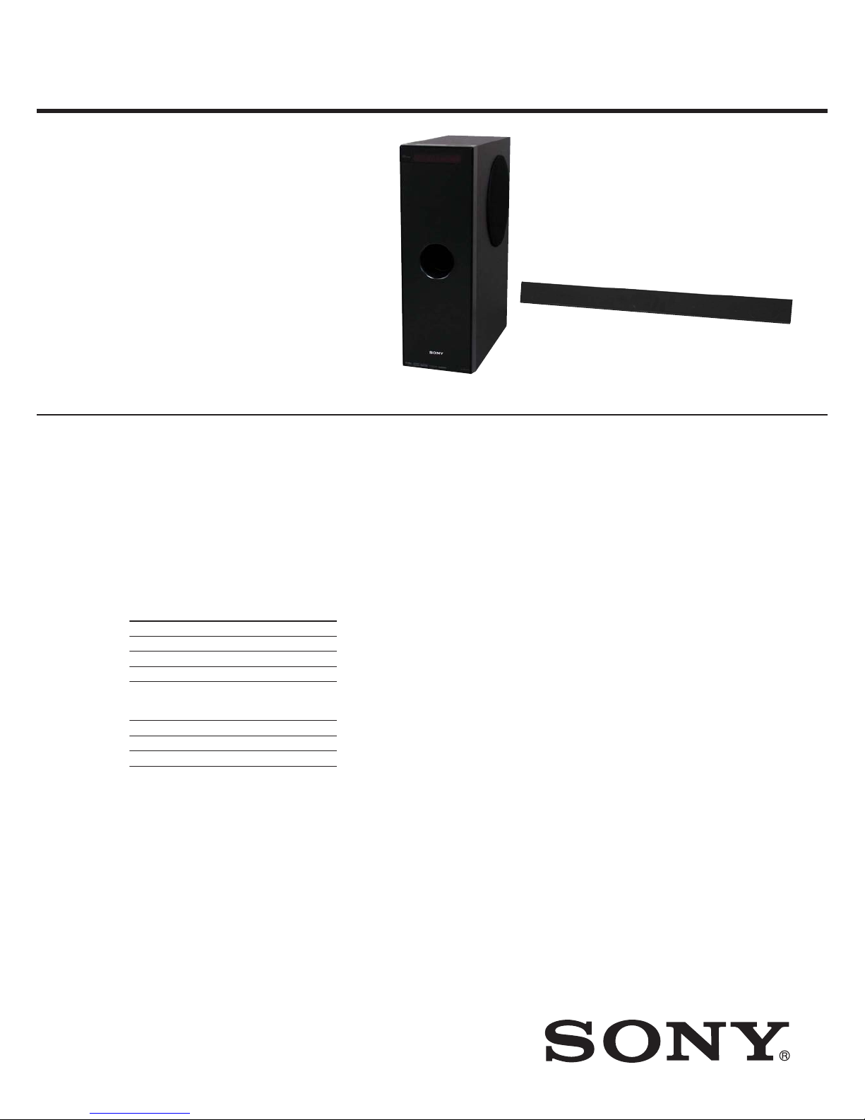
Sony SA-WCT100 User manual

SERVICE MANUAL
Sony Corporation
Audio Business Group
Published by Sony Techno Create Corporation
SA-WCT100/SS-MCT100
SPECIFICATIONS
SA-WCT100
ACTIVE SUBWOOFER
SS-MCT100
SPEAKER SYSTEM
9-887-974-01
2008B05-1
© 2008.02
US Model
Canadian Model
Ver. 1.0 2008.02
• SA-WCT100 is the amplifier, HDMI and active sub-
woofer section in HT-CT100.
• SS-MCT100 is the satellite speaker in HT-CT100.
• Repair in the state of having connected with SA-
WCT100 and SS-MCT100.
This system incorporates Dolby* Digital and Pro Logic Surround and the DTS** Digital Surround System.
* Manufactured under license from Dolby Laboratories.
Dolby, Pro Logic and the double-D symbol are trademarks of Dolby Laboratories.
**Manufactured under license under U.S. Patent
6,487,535 & other U.S. and worldwide patents #'s: 5,451,942; 5,956,674; 5,974,380; 5,978,762; issued & pending. DTS and DTS Digital
Surround are registered trademarks and the DTS logos and Symbol are trademarks of DTS, Inc. © 1996-2007 DTS, Inc. All Rights Reserved.
This system incorporates High-Definition Multimedia Interface (HDMI™) technology.
HDMI, the HDMI logo and High-Definition Multimedia Interface are trademarks or registered trademarks of HDMI Licensing LLC.
“BRAVIA” is a trademark of Sony Corporation.
Photo: SA-WCT100 Photo: SS-MCT100
Formats supported by this
system
Digital input formats supported by this system
are as follows.
* Linear PCM accepts sampling frequencies of no
more than 48 kHz.
AUDIO POWER SPECIFICATIONS
(SA-WCT100)
POWER OUTPUT AND TOTAL HARMONIC
DISTORTION (Stereo mode):
With 8 ohms loads, both channels driven, from 180 -
20,000 Hz; rated 40 Watts per channel minimum RMS
power, with no more than 1 % total harmonic distortion
from 250 milli Watts to rated output.
Amplifier section (SA-WCT100)
Reference Output Power
Surround mode Front: 50 Watts/ch
(8 ohms at 1 kHz,
THD 10 %)
Center*: 50 Watts/ch
(8 ohms at 1 kHz, THD
10 %)
Subwoofer: 100 Watts/ch
(4 ohms at 100 Hz,
THD 10 %)
* Depending on the sound field settings and the source,
there may be no sound output.
Inputs (Analog)
TV Impedance: 30 kohms
Inputs (Digital)
TV, DVD Optical
SAT Coaxial, optical
HDMI section (SA-WCT100)
Connector HDMI 19pin-standard
connector
Video inputs/outputs BD, DVD, SAT:
640 × 480p@60 Hz
(pixel sent 2 times)
60 Hz
60 Hz
720 × 576p@50 Hz
1440 × 576p@50 Hz
(pixel sent 2 times)
Format Supported/Not supported
Dolby Digital B
DTS B
Linear PCM (2ch)* B
Linear PCM (5.1ch,
7.1ch)* (Only on
HDMI)
B
Dolby Digital Plus ×
Dolby True HD ×
DTS-HD ×
– Continued on next page –

SA-WCT100/SS-MCT100
2
SAFETY CHECK-OUT
After correcting the original service problem, perform the follow-
ing safety check before releasing the set to the customer:
Check the antenna terminals, metal trim, “metallized” knobs,
screws, and all other exposed metal parts for AC leakage.
Check leakage as described below.
LEAKAGE TEST
The AC leakage from any exposed metal part to earth ground and
from all exposed metal parts to any exposed metal part having a
return to chassis, must not exceed 0.5 mA (500 microamperes.).
Leakage current can be measured by any one of three methods.
1. Acommercial leakage tester, such as the Simpson 229 or RCA
WT-540A. Follow the manufacturers’ instructions to use these
instruments.
2. A battery-operated AC milliammeter. The Data Precision 245
digital multimeter is suitable for this job.
3. Measuring the voltage drop across a resistor by means of a
VOM or battery-operatedAC voltmeter. The “limit” indication
is 0.75 V, so analog meters must have an accurate low-voltage
scale. The Simpson 250 and Sanwa SH-63Trd are examples
of a passive VOM that is suitable. Nearly all battery operated
digital multimeters that have a 2 VAC range are suitable. (See
Fig. A)
Fig. A. Using an AC voltmeter to check AC leakage.
1.5 kΩ0.15 μFAC
voltmeter
(0.75 V)
To Exposed Metal
Parts on Set
Earth Ground
Notes on chip component replacement
• Never reuse a disconnected chip component.
• Notice that the minus side of a tantalum capacitor may be dam-
aged by heat.
SAFETY-RELATED COMPONET WARNING!
COMPONENTS IDENTIFIED BY MARK 0OR DOTTED LINE
WITH MARK 0ON THE SCHEMATIC DIAGRAMS AND IN
THE PARTS LIST ARE CRITICAL TO SAFE OPERATION.
REPLACE THESE COMPONENTS WITH SONY PARTS
WHOSE PART NUMBERS APPEAR AS SHOWN IN THIS
MANUAL OR IN SUPPLEMENTS PUBLISHED BY SONY.
ATTENTION AU COMPOSANT AYANT RAPPORT
À LA SÉCURITÉ!
LES COMPOSANTS IDENTIFIÉS PAR UNE MARQUE 0SUR
LES DIAGRAMMES SCHÉMATIQUES ET LA LISTE DES
PIÈCES SONT CRITIQUES POUR LA SÉCURITÉ DE FONC-
TIONNEMENT. NE REMPLACER CES COM- POSANTS QUE
PAR DES PIÈCES SONY DONT LES NUMÉROS SONT DON-
NÉS DANS CE MANUEL OU DANS LES SUPPLÉMENTS
PUBLIÉS PAR SONY.
1280 × 720p@50 Hz
1920 × 1080i@50 Hz
1920 × 1080p@50 Hz
1920 × 1080p@24 Hz
Audio inputs BD, DVD, SAT: Linear
PCM 7.1ch/
Dolby Digital/DTS
Satellite
speaker (SS-MCT100)
Speaker system Bass reflex, magnetically
shielded
Speaker units 40 × 70 mm (1 5/8×27/8
inches) cone type
Dimensions (approx.) 800 × 68 × 65 mm (31 1/2×
23/4×25/8inches) (w/h/d)
Mass (approx.) 2 kg (4 lb 7 oz)
Active subwoofer (SA-WCT100)
Speaker system Bass reflex
Speaker unit 160 mm (6 1/2inches) cone
type
Dimensions (approx.) 160 × 500 × 360 mm (6 3/8
×193/4×141/4inches)
(w/h/d)
Mass (approx.) 10 kg (22 lb 1 oz)
Power requirements AC 120 V/60 Hz
Power consumption
Design and specifications are subject to change without
notice.
On:70Watts
Active Standby (Control for HDMI is on):
Signal in: 5 Watts (maximum)
No signal: 1.5 Watts (minimum)
Standby (Control for HDMI is off): 0.3 Watts

SA-WCT100/SS-MCT100
3
1. SERVICING NOTES ............................................... 4
2. GENERAL .................................................................. 6
3. DISASSEMBLY
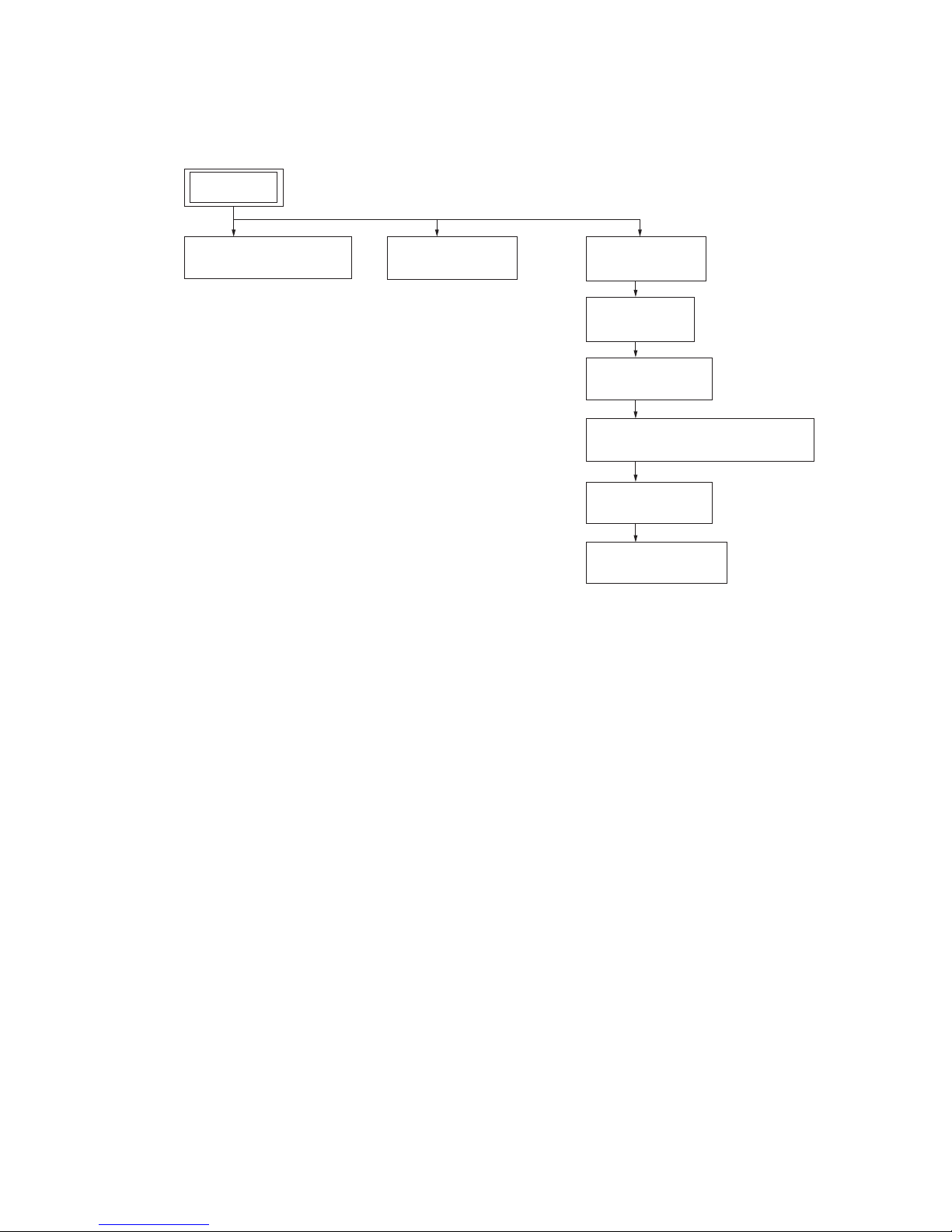
3-1. Disassembly Flow........................................................... 7
3-2. Front Panel Assy............................................................. 8
3-3. Grille Assy ...................................................................... 9
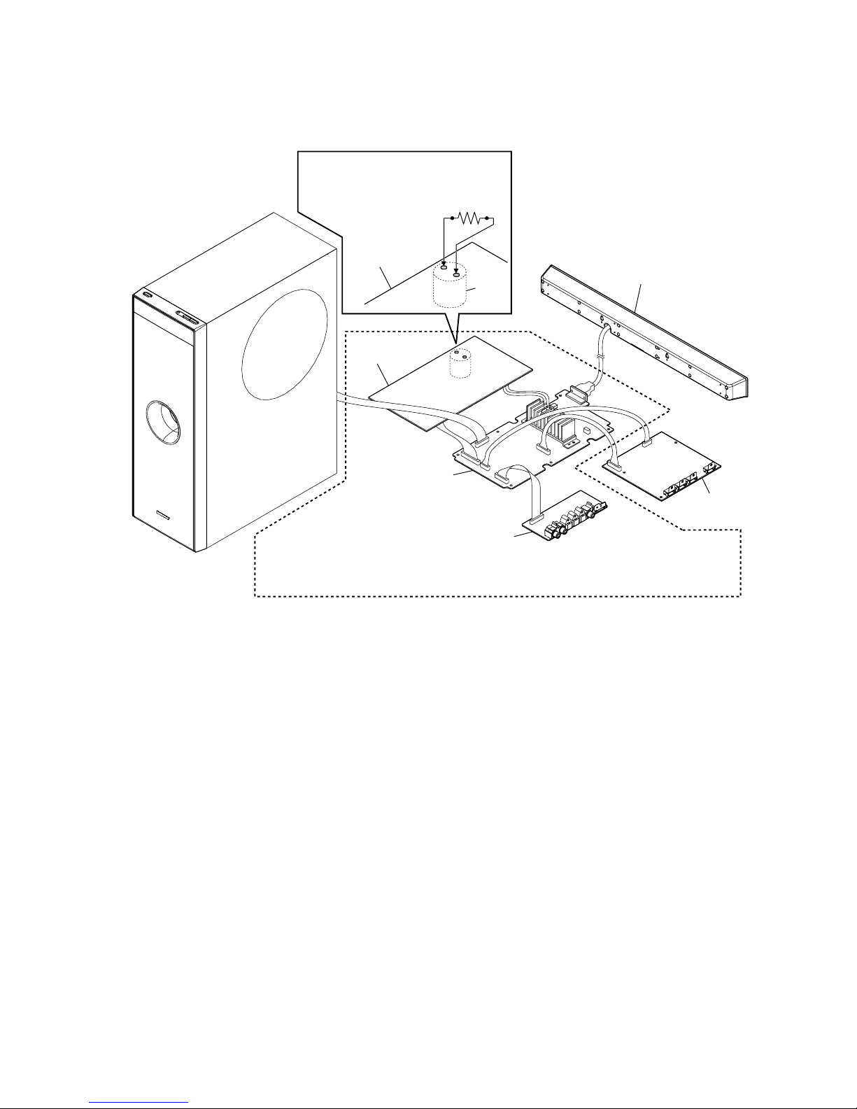
3-4. AMP Block ..................................................................... 10
3-5. IO Board ......................................................................... 10
3-6. HDMI Board................................................................... 11
3-7. Back Panel, D.C. FAN (M3001)..................................... 11
3-8. MAIN Board................................................................... 12
3-9. POWER Board................................................................ 12
4. TEST MODE ............................................................. 13
5. DIAGRAMS
5-1. Block Diagram - MAIN Section (SA-WCT100) -.......... 14
5-2. Block Diagram - HDMI Section (SA-WCT100) -.......... 15
5-3. Block Diagram - AMP Section (SA-WCT100) -............ 16
5-4. Block Diagram - POWER SUPPLY Section -................ 17
5-5. Schematic Diagram
- MAIN Board (1/7) (SA-WCT100) -............................. 19
5-6. Schematic Diagram
- MAIN Board (2/7) (SA-WCT100) -............................. 20
5-7. Schematic Diagram
- MAIN Board (3/7) (SA-WCT100) -............................. 21
5-8. Schematic Diagram
- MAIN Board (4/7) (SA-WCT100) -............................. 22
5-9. Schematic Diagram
- MAIN Board (5/7) (SA-WCT100) -............................. 23
5-10. Schematic Diagram
- MAIN Board (6/7) (SA-WCT100) -............................. 24
5-11. Schematic Diagram
- MAIN Board (7/7) (SA-WCT100) -............................. 25
5-12. Printed Wiring Board
- MAIN Board (Component Side) (SA-WCT100) -....... 26
5-13. Printed Wiring Board
- MAIN Board (Conductor Side) (SA-WCT100) -......... 27
5-14. Printed Wiring Board - IO Board (SA-WCT100) - ........ 28
5-15. Schematic Diagram - IO Board (SA-WCT100) -........... 29
5-16. Printed Wiring Board
- HDMI Board (Side A) (SA-WCT100) -....................... 30
5-17. Printed Wiring Board
- HDMI Board (Side B) (SA-WCT100) -....................... 31
5-18. Schematic Diagram
- HDMI Board (1/2) (SA-WCT100) -............................. 32
5-19. Schematic Diagram
- HDMI Board (2/2) (SA-WCT100) -............................. 33
5-20. Printed Wiring Board
- SPOUT Board (SA-WCT100) - ................................... 34
5-21. Schematic Diagram
- SPOUT Board (SA-WCT100) - ................................... 34
5-22. Printed Wiring Board
- REMOTE Board (SS-MCT100) - ................................ 34
5-23. Schematic Diagram
- REMOTE Board (SS-MCT100) - ................................ 34
5-24. Printed Wiring Board
- DISPLAY Board (SA-WCT100) -................................ 35
5-25. Schematic Diagram
- DISPLAY Board (SA-WCT100) -................................ 36
5-26. Printed Wiring Boards
- PANEL Section (SA-WCT100) - ................................. 37
5-27. Schematic Diagram
- PANEL Section (SA-WCT100) - ................................. 37
TABLE OF CONTENTS
5-28. Printed Wiring Board
- POWER Board (SA-WCT100) -.................................. 38
5-29. Schematic Diagram
- POWER Board (SA-WCT100) -................................. 39
6. EXPLODED VIEWS
6-1. Cabinet Section (SA-WCT100)...................................... 58
6-2. Front Panel Section (SA-WCT100)................................ 59
6-3. AMP Section (SA-WCT100).......................................... 60
6-4. Main Section (SA-WCT100).......................................... 61
6-5. SS-MCT100.................................................................... 62
7. ELECTRICAL PARTS LIST .............................. 63

SA-WCT100/SS-MCT100
4
SECTION 1
SERVICING NOTES
UNLEADED SOLDER
Boards requiring use of unleaded solder are printed with the lead-
free mark (LF) indicating the solder contains no lead.
(Caution: Some printed circuit boards may not come printed with
the lead free mark due to their particular size)
: LEAD FREE MARK
Unleaded solder has the following characteristics.
• Unleaded solder melts at a temperature about 40 °C higher
than ordinary solder.
Ordinary soldering irons can be used but the iron tip has to be
applied to the solder joint for a slightly longer time.
Soldering irons using a temperature regulator should be set to
about 350 °C.
Caution: The printed pattern (copper foil) may peel away if the
heated tip is applied for too long, so be careful!
• Strong viscosity
Unleaded solder is more viscous (sticky, less prone to flow)
than ordinary solder so use caution not to let solder bridges
occur such as on IC pins, etc.
• Usable with ordinary solder
It is best to use only unleaded solder but unleaded solder may
also be added to ordinary solder.
NOTE OF REPAIR CONFIRMING
Repair in the state of having connected with SA-WCT100 and SS-
MCT100.
NOTE THE IC3511 and IC3513 ON THE HDMI BOARD
REPLACING
When IC3511 and IC3513 cannot exchange with single. When
IC3511 and IC3513 are damaged, exchange the entire mounted
board.
• JIG
When disassembling the set, use the following jig (for speaker
removal).
Part No.: J-2501-238-A
JIG FOR SPEAKER REMOVAL

SA-WCT100/SS-MCT100
5
SERVICE POSITION
IO board
SS-MCT100
HDMI board
MAIN board
POWER board
POWER board
C903
800 Ω/2W
Note 2: In checking the board, make
a capacitor discharge of C903
for electric shock prevention.
Note 4: SA-WCT100 is connected with SS-MCT100,
and remote commander is operation.
If SS-MCT100 is not connected,
remote commander cannot be operation.
Note 3: Connect the IO board and the POWER board with the MAIN board when turning on power.
Otherwise, the IC of MAIN board is damaged, and the POWER board is protected.
Note 1: Take all board out from SA-WCT100 and connect each board.

SA-WCT100/SS-MCT100
6
SECTION 2
GENERAL Thia section is extracted from
instruction manual.
Top panel (Active subwoofer)
A?/1 (on/standby)
Press to turn the system on or off.
BINPUT SELECTOR
Press to select the input source to play back.
CVOLUME +/–
Press to adjust the volume level.
INPUT SELECTOR
-
VOLUME +
Front panel display (Active subwoofer)
About the indications in the front panel display
APOWER / ACTIVE STANDBY indicator
Lights as follows:
Green: The system is turned on.
Amber: Control for HDMI function is
working while the system is turned
off.
Off: The system is turned off, and the
Control for HDMI function is not
working.
BLights up according to the audio input
signals.
CSLEEP
Flashes when the sleep timer function is
active.
DHDMI
Lights up when the HDMI equipment is
being used.
ECOAX/OPT
Lights up according to the cable which you
are using.
POWER /
ACTIVE STANDBY
Remote control
Here describes the buttons for amplifier
operation only.
• Point the remote at the remote sensor on the
satellite speaker.
*The5,)and MASTER VOL + buttons have a
tactile dot. Use it as a guide during operation.
" (on/standby)
Press to turn the system on or off.
#Input buttons
Press one of the buttons to select the
componentyouwanttouse.
The buttons are factory assigned to control
Sony components. You can change the
factory settings of the input buttons to suit
the components in your system. For details,
refer to “Changing the input button
assignments of the remote”.
$SOUND FIELD
Press to select the sound field.
%LEVEL MODE
Presstoadjust thelevelofthecenterspeaker
and the subwoofer.
& MENU
Press to display the menu of the system.
'MUTING
Presstoturnoffthesound.
(MASTER VOL +/–
Press to adjust the volume.
)$,9,Y,Dor
Press $,9,Yor Dto select the settings.
Then press to enter the selection.
Note
123
46
78
0
ENTER
9
TV INPUTTHEATER TV
AV
TV BD DVD SAT
SYSTEM STANDBY
TOP MENU MENU
BD/DVD
RETURN/EXIT
TV
REPLAY ADVANCE
MENU/HOME
F1 F2
AMP MENU
CLEAR
TOOLS/
OPTIONS
DISPLAY MUTING
TV VOL
MASTER VOL
SOUND
FIELD
LEVEL
MODE
GUIDE
FAVORITEWIDEPICTUREJUMP
DMPORT
+HCVT-HCVT
'
(H
G
).N
9Y
5

SA-WCT100/SS-MCT100
7
SECTION 3
DISASSEMBLY
• This set can be disassembled in the order shown below.
3-1. DISASSEMBLY FLOW (SA-WCT100)
3-2. FRONT PANEL ASSY
(Page 8) 3-3. GRILLE ASSY
(Page 9) 3-4. AMP BLOCK
(Page 10)
3-5. IO BOARD
(Page 10)
3-6. HDMI BOARD
(Page 11)
3-9. POWER BOARD
(Page 12)
3-7. BACK PANEL, D.C. FAN (M3001)
(Page 11)
3-8. MAIN BOARD
(Page 12)
SET

SA-WCT100/SS-MCT100
8
Note: Follow the disassembly procedure in the numerical order given.
3-2. FRONT PANEL ASSY
Note: Please do set by placing the grille assy side up as shown in the figure and work.
wire (flat type) (15 core)
(CN801)
sheet (wire vibration proof)
Insert the jig (J-2501-238-A) into a space
made by inserting the screwdriver,
and raise the front panel assy gradually.
Insert the jig (J-2501-238-A) into a space
made by inserting the screwdriver,
and raise the front panel assy gradually.
Raise the front panel assy a little by little
from bottom to top of the set.
eight bosses
bottom side
Insert a flat-tip screwdriver into a recess
in the bottom of the set
to raise the front panel assy a little.
two screws
(BVTP3
×8)
two screws
(BVTP3
×8)
R front panel assy
retainer board
retainer board
ferrite core

SA-WCT100/SS-MCT100
9
3-3. GRILLE ASSY
Note: Please do set by placing the grille assy side up as shown in the figure and work.
Insert the jig (J-2501-238-A) into a space
made by inserting the screwdriver,
and raise the grille assy gradually.
grille assy
Insert a flat-tip screwdriver into a recess
in the bottom of the grille assy
to raise the front panel assy a little.
grille assy
boss boss
boss
boss
bottom side

SA-WCT100/SS-MCT100
10
3-4. AMP BLOCK
five screws
(4
×20)
connector
(CN252)
AMP block
3-5. IO BOARD
twelve screws
(BVTP3
×8)
bracket (top)
screw
(BVTP3
×8)
five screws
(BVTP3
×8)
screw
(BVTT3
×6)
IO board
wire (flat type) (19 core)
(IO board: CN202/MAIN board: CN1018)

SA-WCT100/SS-MCT100
11
3-6. HDMI BOARD
four screws
(BVTP3
×8)
two screws
(BVTP3
×8)
wire (flat type) (17 core)
(HDMI board: CN3511/
MAIN board: CN1004)
harness
(HDMI board: CN3509/
MAIN board: CN1005)
screw
(BVTP3
×8)
left HDMI bracket
HDMI board
three screws
(BVTP3
×8)
3-7. BACK PANEL, D.C. FAN (M3001)
eight screws
(BVTP3
×8)
two screws
(BVTP3
×8)
two bolts
back panel
connector
(CN3007)
D.C.fan (50 square)
(M3001)

SA-WCT100/SS-MCT100
12
3-8. MAIN BOARD
two screws (BVTP3 ×8)
heat sink radiation sheet
six screws
(BVTP3
×8)
seven screws
(BVTP3
×8)
MAIN board
two connectors
(CN3003,CN3005)
connector
(CN1002)
bracket (shield)
3-9. POWER BOARD
five screws
(BVTP3
×8)
PC board holder
POWER board two screws
(BVTP3
×8)
connector (CN901)

SA-WCT100/SS-MCT100
SA-WCT100/SS-MCT100
1313
2-8. Digital Media Port Test
Note: SA-WCT100 is connected with SS-MCT100, and remote com-
mander is operation. If SS-MCT100 is not connected, remote
commander cannot be operation.
Procedure:
1. Connect the DMPORT check jig (P/N: J-2501-309-A) with the
DMPORT jack (CN204) on the IO board.
2. Press the [?/1] button to turn the power on.
3. Confirm that both LEDs of the DMPORT check jig lights.
(Confirmation the power supply line.)
4. Press the [INPUT SELECTOR] button to select the “DMPORT”.
5. Enter the test menu.
6. Press the [VOLUME +] and [VOLUME –] buttons to select
the “DMPORT CHK”, and press the [INPUT SELECTOR]
button.
7. The message “DMPORT OK.” appears on the fluorescent indi-
cator tube and enter the digital media port test mode. (Confir-
mation of communication line)
When “NO DETECT.” and “UART .TO” are displayed on
the fluorescent indicator tube, confirm the connection of the
DMPORT check jig, and enter the mode again.
Each time the [>] button on the remote commander is
pressed, the connect check and adaptor version check are
changed.
Press the [.] button on the remote commander, connected
confirmation of the DMPORT check jig is done again.
8. To a pinjack of the DMPORT check jig input information rel-
evant to audio signal (sine-wave 1.0V rms).
9. Confirm the output of speakers. (Confirmation of analog sig-
nal)
10. To release from this mode, press the [?/1] button.
2-9. Cold Reset
Execute this mode when returning the set to the customers.
Procedure:
1. Enter the test menu.
2. Press the [VOLUME +] and [VOLUME –] buttons to select
the “COLD RESET”, and press the [INPUT SELECTOR] but-
ton.
3. The message “COLD RESET.” appears on the fluorescent in-
dicator tube, then turn the power off.
AF
oscillator
DMPORT
check jig
(Part No.:
J-2501-309-A)
J001
SA-WCT100 SS-MCT100
IO board
CN204 MAIN board
CN3008
SECTION 4
TEST MODE
1. TEST MODES OTHER THAN THE TEST MENU
These are executable test mode even if not entering the test menu.
1-1. Cold Reset
Procedure:
1. Press the [?/1] button to turn the power on.
2. Press the three buttons [VOLUME –], [INPUT SELECTOR]
and [?/1] simultaneously.
3. The message “COLD RESET” appears on the fluorescent indi-
cator tube, then turn the power off.
1-2. HDMI Version Display
Procedure:
1. Press the [?/1] button to turn the power on.
2. Press and hold down the two buttons [VOLUME –] and [IN-
PUT SELECTOR] simultaneously (around 5 seconds).
3. The message “hdmi XX.XX” or “HDMI XX.XX” appears on
the fluorescent indicator tube.
Note: XX.XX is HDMI microprocessor version.
2. TEST MODES IN THE TEST MENU
These are the test modes done in the test menu.
Setting method of the test menu:
1. Press the [?/1] button to turn the power on.
2. Press and hold down the two buttons [VOLUME +] and [IN-
PUT SELECTOR] simultaneously (around 5 seconds).
3. The message “TEST MENU” appears on the fluorescent indi-
cator tube and enter the test menu.
2-1. Panel Test
Procedure:
1. Enter the test menu.
2. Press the [VOLUME +] and [VOLUME –] buttons to select
the “PANEL”, and press the [INPUT SELECTOR] button.
3. All segments in fluorescent indicator tube are lighted up. And
half segments in fluorescent indicator tube are lighted up,
others half segments in fluorescent indicator tube are lighted
up, then all segments in fluorescent indicator tube are lighted
up. Or HDMI indicator LED (amber) is lighted up and down.
These operation is repeated.
4. When all segments in fluorescent indicator tube are lighted up
in the state of step 3, press the [VOLUME +] button and model
information is displayed on the fluorescent indicator tube.
Each time the [VOLUME +] button is pressed, the display
changes from destination information, MC version, SYS ver-
sion, UI version, TA version, DSP version, TM version, CLA
version, CEC version in this order, and returns to the model
information display.
5. In the state of step 3, press the [VOLUME –] button and “K 0”
is displayed on the fluorescent indicator tube.
“K 0” value increases whenever a button on the set is pressed.
However, once a button has been pressed, it is no longer taken
into account.
All buttons on the set is pressed, “OK” and “K 4” are alter-
nately displayed on the fluorescent indicator tube.
6. To release from this mode, press the [?/1] button.
2-2. Tone Test
Procedure:
1. Enter the test menu.
2. Press the [VOLUME +] and [VOLUME –] buttons to select
the “TONE TEST”, and press the [INPUT SELECTOR] but-
ton.
3. The message “T. TONE ON” appears on the fluorescent indi-
cator tube and enter the tone test mode.
Then the message “T. TONE FL”, “T. TONE CEN”, “T.
TONE FR”, and “T. TONE SW” is displayed repeatedly. At
the same time, the speaker output is chaged according to the
display.
4. To release from this mode, press the [?/1] button.
2-3. AMP Test
Not used for the servicing.
Press the [?/1] button if having entered this mode.
2-4. DSP Halt Mode
Not used for the servicing.
Press the [?/1] button if having entered this mode.
2-5. VACS On/off
Not used for the servicing.
Press the [?/1] button if having entered this mode.
2-6. VACS Display
Not used for the servicing.
Press the [?/1] button if having entered this mode.
2-7. DMPORT Device Test
Not used for the servicing.
Press the [?/1] button if having entered this mode.

SA-WCT100/SS-MCT100
SA-WCT100/SS-MCT100
1414
5-1. BLOCK DIAGRAM - MAIN Section (SA-WCT100) -
BUFFER
IC207
BUFFER
IC209
5V
REGULATOR
IC208
SYSTEM CONTROLLER
IC1002 (2/4)
OPTICAL
RECEIVER
IC201
10
A9
B
X2
15
X1
14
AINL
2
DPSIA
DIR_XSTATE
DATA_AD
DIR_BCK
DIR_MCK
DIR_LRCK
78
NONAUDIO*
DIR_NONAU 97
DIN0
3
DIR DO
66
DSP_MOSI/DIR_DIN
5
DSP_SPICLK/DIR CLK
7
DIR CE
68
DIR ERROR
27
DIR_RST
69
DIR XSTATE
67
DIR_ZERO
ROM_SDA1
ROM_SCL1
XCEC_DI
CEC_DO
18
A_SEL0
A_SEL1
A_SEL2
A_SEL0
A_SEL1
A_SEL2
A_SEL0
A_SEL1
A_SEL2
DIA_ERR
16
MOSI
127
MISO
126
SPICLK
125
SPIDS*
122
RESET*
121
INT_REQ
15
SDTO 9
SCLK 12
LRCK 10
MCLK 11
X13
DO 35
DI 36
CL(I) 38
CE 37
ERROR(O) 34
XMODE 48
XSTATE(O)
DIR_DO
DIR_ZERO
DIR_CSFLAG
SPDIF
DSP_MOSI
DSP_SPICLK
DIR_CE
DIR_ERROR
DIR_RST
DIR_XSTATE
DIR_DO
DIR_ZERO
DSP_MOSI
DSP_SPICLK
DIR_CE
DIR_ERROR
DIR_CSFLAG
DIR_RST
DIR_XSTATE
17
DATA0(O) 16 DPSOA 64
DPSOC 70
DPDVLRCK 86
DPDVBCK 87
BCK(O) 14
LRCK(O) 15
CKOUT 13
AUDIO(O) 24
CSFLAG(O) 25
OPT
SAT
1 2 14
1G B A
50 51 52
DSP_MISO
6
DSP SPIDS
DSP RST
DSP_INTR
73 72 71
1Y 7
1C0
6
1C2
4
OPTICAL
RECEIVER
IC202
DVD
OPT
1C3
3
OPTICAL
RECEIVER
IC203
TV
OPT
SCHMITT
TRIGGER
IC206
DIGITALAUDIO
INTERFACE RECEIVER
IC1011
DIGITALAUDIO
INPUT SELECTOR
IC204
DSP
IC2
DIN1
J201 4
COAX
CEC DATA
SWITCH
Q1004-1007
32253 54
INVERTER
Q201, 202
INPUT
TV L
R R-CH
R-CH
+6V
SW+3.3V
ANALOGAUDIO
INPUT SELECT
IC205
A/D CONVERTER
IC1208
PDN 13 DIR_RST
21
22
X1002
12.288MHz
XOUT(O)
XIN(I)
DIR_CSFLAG
19
vSIGNAL PATH
: AUDIO (ANALOG)
: AUDIO (DIGITAL)
vR-ch is omitted due to same as L-ch.
AF
B
E
DIN2
5
D1FLFR
D3CSW
DSP_BCK
CEC
DPDVLRCK
C
142
143
X1
25MHz
CLKIN
XTAL
13 15
X1001
5MHz
XOUT XIN
CN204
DMPORT
Lch
Rch
VBUS(5V)
VIDEO5V
RXD
TXD
DET
RX
TX
DET
DMPORT_RX_IN
DMPORT_TX_OUT
DMPORT_DET
13
14
2
4
5
6
7
32
31
49
79 DPSIB
94 DPFSCK
89 DPLBCK
88 DPLRCK
81 DPSID
82 DPSIE
80 DPSIC
LRCK
DPSIB
MCK
BCK
DPSID
DPSIE
DPSIC
D1FLFR, D3CSW,
DPDVLRCK,
DSP_BCK
DIR_XSTAE, DIR_LRCK,
DIR_MCK, DIR_BCK, DATA_AD
EEPROM
IC1013
SECTION 5
DIAGRAMS
(Page 15) (Page 15)
(Page 15)
(Page 16)
(Page 15)

SA-WCT100/SS-MCT100
SA-WCT100/SS-MCT100
1515
5-2. BLOCK DIAGRAM - HDMI Section (SA-WCT100) -
• SIGNAL PATH
: AUDIO (DIGITAL)
: VIDEO
HDMI CONTROLLER
IC3519
CN3501
SAT IN
A32
52 B32
51
7
9
A33
55 B33
54
4
6
A34
58 B34
57
1
3
A31
49 B31
48
10
DATA0+
DATA0-
DATA1+
DATA1-
DATA2+
DATA2-
CLOCK+
CLOCK-
SDA(5V)
SCL(5V)
+5V POWER
HOT PLUG DET
18
CEC 13
12
16
15
HDMI
INPUT
SELECTOR
IC3503
56
P5V_SELB
55
P5V_SELA
SDA3
45
19 HPD3
44
SCL3
46
CN3502
DVD INHDMI
A22
71 B22
70
7
9
A23
74 B23
73
4
6
A24
77 B24
76
1
3
A21
68 B21
67
10
DATA0+
DATA0-
DATA1+
DATA1-
DATA2+
DATA2-
CLOCK+
CLOCK-
SDA(5V)
SCL(5V)
+5V POWER
HOT PLUG DET
18
CEC 13
12
16
15 SDA2
63
19 HPD2
62
SCL2
64
CN3503
BD IN
A12
9B12
8
7
9
A13
12 B13
11
4
6
A14
15 B14
14
1
3
A11
6B11
5
10
DATA0+
DATA0-
DATA1+
DATA1-
DATA2+
DATA2-
CLOCK+
CLOCK-
SDA(5V)
SCL(5V)
+5V POWER
HOT PLUG DET
18
CEC 13
12
16
15 SDA1
2
19 HPD1
80
SCL1
3
RX_HPD1
HDMI RECEIVER
IC3511
HDMI
TRANSCEIVER
IC3513
Y1 34
Z1 35 51
50
Y2 31
Z2 32 55
54
Y3 28
Z3 29 59
58
Y4 25
Z4 26 63
RXC+
RXC-
RX0+
RX0-
RX1+
RX1-
RX2+
RX2-
DSDA
DSCL
62
41
PWR5V
44
42
CSDA
CSCL
39
40
SCL_SINK 38
HPD_SINK 40
OE 42
SDA_SINK 39
S1 21
S2 22
S3 23
LEVEL
SHIFT
IC3501
(1/2)
LEVEL
SHIFT
IC3507
S [1]
S [2]
S [3]
SIGNALSELECTOR
IC3504
2Y2
22Y3
42Y1
53
2-COM
10 9
AB
21 51 52 53
S [1]
S [2]
S [3]
TMDS_S1
TMDS_S2
TMDS_S3
DATASELECTOR
IC3521 EEPROM
IC3509
2Y1
52Y0
1
1Y1
14 1Y0
12
3
2-COM
13
1-COM
5SDA
6SCL
EEPROMSEL1
10
A7
WP
35
TMS_0EB
54
RX_RST
19
MUTE
65
RX_INT
20
TX_INT
43
TX_5VPWR
41
TX_RST
PCM_MULTI
42
CSCL
27
CSDA
CSCL
CSDA
CSCL
CSDA
28
124 - 121,117 - 114,
111 - 108, 105 - 99,
96 - 92
QE0 - QE23
79 - 75, 70 - 67
65 - 61, 58 - 49
D0 - D23
ODCK 119
HSYNC 128
VSYNC 1
DE 127
SPDIF 70
SD0 - SD3 4
24
MCLK 79
SCK 76
WS 75
MUTE 67
RESET 89
INT
RESET
RX_INT
RESET
RX_INT
91
IDCK
66 HSYNC
1VSYNC
2DE
80
74 - 71
SPDIF
5
SD0 - SD3
MCLK
6SCK
12 WS
11
10 - 7
TX0+ 30
TX0- 29 7
9
TX1+ 33
TX1- 32 4
6
TX2+ 36
TX2- 35 1
3
TXC+ 27
TXC- 26 10
HPD
DATA0+
DATA0-
DATA1+
DATA1-
DATA2+
DATA2-
CLOCK+
CLOCK-
SDA(5V)
SCL(5V)
HOT PLUG DET
+5V POWER
18 19
12
16
15
13
18
DSDA 19
DSCL 20
INT 17
RESET 42
CSDA 44
CSCL 43
LEVEL
SHIFT
IC3501 (2/2)
+6V
LEVEL
SHIFT
Q3504
CN3504
HDMI
TV OUT
TX_INT
TX_RST
TX_INT
TX_RST
14 12
4A
13 4B
10 3B
11 3A
62B
52A
31B
21A
4Y
93Y
2Y
SEL
1
SELECTOR
IC1014
7
1Y 4
DATA_AD
SPDIFSPDIF
MCK
SD0
LRCK
DPSIB
MCK
BCK
LRCK
DIR_LRCK
MCK
DIR_MCK
BCK
DIR_BCK
14 12
4A
13 4B
31B
21A
62B
2A
10 3B
3A
4Y
41Y
2Y
SEL
1
70
SELECTOR
IC1015
SYSTEM CONTROL
IC1002 (1/4)
7
3Y 9
SPDIF
LRCK
MCK
BCK
SD0 - SD3
DIR_XSTAE EMG_MUTE
MCK,
EMG_MUTE
SD2
SD3
SD1
DPSID
DPSIE
DPSIC
5
11
RXD0
36 TXD0
35 HRESET
37 HDMI_MUTE
38
85
84
XTALIN
XTALOUT
X3501
28.322MHz
DIR_XSTAE, DIR_LRCK,
DIR_MCK, DIR_BCK, DATA_AD
13
11
XIN
XOUT
X3502
10MHz
34RX 33TX 10RESET
C
B
A
F
D
CEC
LEVELSHIFT
Q1008
SWITCH
Q3505 - 3507
+5V REGLATOR
IC3516
(Page 14)
(Page 14)
(Page 14)
(Page
14)
(Page 16)

SA-WCT100/SS-MCT100
SA-WCT100/SS-MCT100
1616
5-3. BLOCK DIAGRAM - AMP Section (SA-WCT100) -
/SD
PWM_B
OUT_A
14
PWM_A
6
4
/RESET
5
25-27
28-30
/SD
PWM_B OUT_B
OUT_A
14
PWM_A
6
4
/RESET
5
25-27
28-30
OUT_B
E
D
D1FLFR, D3CSW,
DPDVLRCK,
DSP_BCK
DSP_BCK
D1FLFR
POWERAMP
IC3056
STREAM PROCESSOR
IC3010
BUFFER
IC783
D FLIP-FLOP
IC782
31 DATA
OVER LOAD
DETECT
Q3151, 3152
SYSTEM CONTROLLER
IC1002 (3/4)
30 BCK
DSP_LRCK 29 LRCK
36 XFSIIN
21 SCDT
SC_DT
EMG_MUTE
MCKMCK, EMG_MUTE
MCK
MCK
DSP_BCK
D3CSW
DSP_LRCK
22 SCSHIFT
SHIFT
23 SCLATCH
LAT1
27 INIT
INIT
24 OVF_R
25 OVF_L
OVF_L
OVF2
X3051
49.1MHz
L.P.F.
L.P.F.
OVF1
19 SOFT MUTE
D
Q
CLK
SOFT MUTE
19 SOFT MUTE
SOFT MUTE
OUTL1 11
OUTL2 9
OUTR1 6
OUTR2 4
XFSOIN 48
FSOCKO 37
XFSOOUT 14
FSOI 38
STREAM PROCESSOR
IC3030
31 DATA
30 BCK
29 LRCK
36 XFSIIN
21 SCDT
SC_DT
22 SCSHIFT
SHIFT
23 SCLATCH
LAT3
27 INIT
INIT
24 OVF_R
SC_DT
SC_SHIFT
LAT1
LAT3
NS_INIT
25
OVF1
OUTR1 6
OUTR2 4
OUTL1 11
OUTL2 9
XFSOIN 48
FSOI 38
CLOCK
BUFFER
IC3051
OVER LOAD
DETECT
Q3101, 3102
L.P.F.
L.P.F.
OVER LOAD
DETECT
Q3301, 3302
SP901
OVER LOAD
DETECT
Q3401, 3402
DC DETECT
Q3552, 3553
POWERAMP
IC3400
L.P.F.
L.P.F.
PROTECT DETECT
Q3551
Q781
1
DAMP_SHIFT
DAMP_SCD 2
DAMP LATCH1
DAMP LATCH3
78
80
DAMP INIT 76 OVF1
OVER FLOW1 83 OVF2
OVER FLOW2 84 SOFT MUTE
DAMP SOFT MUTE 77
XDC_DET 85
SIRCS
SIRCS_IN 4
DRIVER RST 81
82
POWERAMP
IC3500
L.P.F.
L.P.F.
• SIGNAL PATH
FAN DRIVE
Q3000 - 3002
D3505
M3001
(FAN)
+12V
D3504
PROTECT DETECT
Q3554 +31.5V
XDRIVER OCP DRIVER_SD
DRIVER_RST
DC_SD
DSP_LRCK
2
1
5
6
4
1
2
7
3
DPDVLRCK
PWM_A OUT_A
OUT_B
433
30
25
22
PWM_B
6
/RST_AB
5
/SD
PWM_C OUT_C
OUT_D
14
PWM_D16
3
/RST_CD
15 E3.3V
L+
L-
R+
R-
C+
C-
SIRCS
E3.3V
CN3008
ONLY FOR
SS-CMT100
SPEAKER
MM
: AUDIO (ANALOG)
: AUDIO (DIGITAL)
(Page 14)
(Page 15)

SA-WCT100/SS-MCT100
SA-WCT100/SS-MCT100
1717
5-4. BLOCK DIAGRAM - POWER SUPPLY Section -
1
4
6
8
FLUORESCENT
INDICATOR TUBE
ND801
T801
DC/DC
CONVERTER
RESET SIGNAL
GENERATOR
IC1006
REMOTE
CONTROL
RECEIVER
IC871
RECT
D802 - 805 OSC
Q803
LED DRIVE
Q802
LED DRIVE
Q801
12RESET
20AC_CUT
LED1
KEY2
KEY1
KEY0
LED2
40
28
23
11 21 24 25
60 62 63 61
P_CONT2
RSTFL_RST/CD
FL_CLK
FL_DATA
FL_CS
CLK
DATA
CS
41P_CONT3
SYSTEM
CONTROLLER
IC1002 (4/4)
FLUORESCENT
INDICATOR TUBE
DRIVER
IC802
D+5V
97
95
94
39P_CONT1
+12V
REGULATOR
IC941
SHUNT
REGULATOR
IC931
+9V
REGULATOR
IC1010
D943
D942
D941L945
L942
L941,
L951
D909
D922
D910
POWER
CONTROL
IC921
T902
SUB POWER
TRANSFORMER
T901
MAIN POWER
TRANSFORMER
65P_CONT4
ISOLATOR
PC902
D931L931 D905 D908
Q943,947
D901
E+4V
E+4V
+31.5V
POWER
CONTROL
IC901
AC IN
SW+3.3V,+3.3V
AMP_3.3V
D+5V
ISOLATOR
PC901
ISOLATOR
PC903
RIPPLE
FILTER
+5V
REGULATOR
IC942
+3.3V
REGULATOR
IC943
+1.8V
REGULATOR
IC3050
+1.8V
REGULATOR
IC3528
+6V
MAIN POWER
ON/OFF SWITCH
B+ SWITCH
Q901
+9V
+12V
D1006
D1007
E3.3V
+1.2V
BUP3.3V
+2.6V
REGULATOR
IC1001
+1.2V
REGULATOR
IC1
+5V
REGULATOR
IC1008
+5V
+1.8V
HDMI+3.3V
HDMI+1.8V
D906, 907
D
VCC
OCP/SYNC
FB/OLP
DRAIN
VCC START UP
FB/OLP
3
4
1
+3.3V
REGULATOR
IC3526
5
3 - 50
(HDMI (AMBER))
POWER/
ACTIVE
STANDBY
(GREEN)
D801
I/
S801
INPUT SELECTOR
S802
VOL–
S803
VOL+
S804
Q921
F901
TH901 LF901, 902
LINE
FILTER
SHUNT
REGULATOR
IC951
RESET
SWITCH
Q1003
+3.3V
REGULATOR
IC3527
CN871
3
SIRCS
(TO SA-WCT100)

SA-WCT100/SS-MCT100
SA-WCT100/SS-MCT100
1818
For Schematic Diagrams.
Note:
• All capacitors are in μF unless otherwise noted. (p: pF) 50
WV or less are not indicated except for electrolytics and
tantalums.
• All resistors are in Ωand 1/4 W or less unless otherwise
specified.
• f: internal component.
• 2: nonflammable resistor.
• 5: fusible resistor.
• C: panel designation.
THIS NOTE IS COMMON FOR PRINTED WIRING BOARDS AND SCHEMATIC DIAGRAMS.
(In addition to this, the necessary note is printed in each block.)
• A: B+ Line.
• B: B– Line.
• Voltages and waveforms are dc with respect to ground
under no-signal conditions.
no mark
: POWER ON
• Voltages are taken with VOM (Input impedance 10 MΩ).
Voltage variations may be noted due to normal production
tolerances.
• Waveforms are taken with a oscilloscope.
Voltage variations may be noted due to normal production
tolerances.
• Circled numbers refer to waveforms.
• Signal path.
J: AUDIO (DIGITAL)
F: AUDIO (ANALOG)
E: VIDEO
For Printed Wiring Boards.
Note:
• X: Parts extracted from the component side.
• Y: parts extracted from the conductor side.
• f: internal component.
• : Pattern from the side which enables seeing.
(The other layers' patterns are not indicated.)
• Indication of transistor.
C
BThese are omitted.
E
Q
Caution:
Parts face side:
(SIDE A)
Pattern face side:
(SIDE B)
Parts on the parts face side seen from
the pattern face are indicated.
Parts on the pattern face side seen from
the parts face are indicated.
Note:
The components identi-
fied by mark 0or dotted
line with mark 0are criti-
cal for safety.
Replace only with part
number specified.
Note:
Les composants identifiés
par une marque 0sont
critiques pour la sécurité.
Ne les remplacer que par
une piéce portant le nu-
méro spécifié.
Caution:
Parts face side:
(Conductor Side)
Pattern face side:
(Component Side)
Parts on the parts face side seen from
the pattern face are indicated.
Parts on the pattern face side seen from
the parts face are indicated.
• HDMI board is multi-layer printed board. However, the
patterns of intermediate layers have not been included in
diagrams.
• Circuit Boards Location
DISPLAY board
TSW board
TSW2 board
SPOUT board
POWER board
MAIN board
HDMI board
IO board
REMOTE board
– SS-MCT100 –
– SA-WCT100 –

SA-WCT100/SS-MCT100
SA-WCT100/SS-MCT100
1919
5-5. SCHEMATIC DIAGRAM - MAIN Board (1/7) (SA-WCT100) - • See Page 40 for IC Block Diagrams.
MAIN
(2/7)
4
BOARD
HDMI
(2/2)
A
BOARD
CN3511
IC B/D
MAIN
5
(2/7)
BOARD
MAIN
15
(3/7)
BOARD
MAIN
BOARD
(3/7)
1
MAIN
BOARD
(7/7)
3
IC B/D
IC B/D
3.3
3.4
3.4
3.4
0.4
0
3.3
1.2
0.2
2
1.7
0
1.7
0
0.2
0
0.4
0
0
1.7
0
1.7
1.7
0
1.7
3.3
4
2.5
1
0
3.4
0.1
C1002
1k
R1012
12345
SI-3010KM-TL
IC1001
VC
VIN
GND
VOUT
ADJ
0.1
C1011
16V
100
C1001
2.6V
DSP_MISO
DSP_INT
SW3.3V
15k
R1023
10k
R1024
SI_C
SI_D
SI_E
SI_B
16 15 14 13 12 11 10 9
87654321
TC74VHC157FT(EKJ)
IC1014
SEL
1A
1B
1Y
2A
2B
2Y
GND 3Y
3B
3A
4Y
4B
4A
ST
VDD
0.1
C1021
100
R1183
100R1184
100
R1185
100
R1180
0.1
C1029
150R48
100R51
100
R52
RT1N141C-TP-1
Q1008
10kR1123
100
R1124
16 15 14 13 12 11 10 9
87654321
TC74VHC157FT(EKJ)
IC1015
SEL
1A
1B
1Y
2A
2B
2Y
GND 3Y
3B
3A
4Y
4B
4A
ST
VDD
EMG_MUTE
LRCK
BCK
MCK
DSP_SPICLK
DSP_MOSI
DSP_RESET
DSP_SPIDS
16V
100
C1012
100k
R1155
1
2
3
4
5
6
7
8
9
10
11
12
13
14
15
16
17
17P
CN1004
GND
GND
HDMI_MCK
GND
HDMI_BCK
HDMI_LRCK
SD3
SD2
SD1
SD0
HDMI-SPDIF
MUTE_REQ
PCONT4
HUART_TX
HUART_RX
HRESET
CEC
0.47uHL1004
R1061 100
R1062 100
R1066 100
R1068 100
R1069 100
100R1119
100
R1125
100
R1126
100
R1127
100
R1120
100
R1121
100
R1122
1kR1077
A1
A2
A3
A4
A5
A6
A7
B1
B2
B3
A0
DSP
HDMI
DGND
DSP_INT
HRESET
HDMI_BCK
HDMI_SD0
HDMI_LRCK
HDMI_MCK
DSP_RESET
DSP_SPIDS
DSP_MISO
DSP_MOSI
DSP_SPICLK
HDMI_SD2
HDMI_SD3
PCONT_DSP
CEC
HRXD
HTXD
PCONT4
HDMI_SD1
DSP_SPICLK
HDMI_SD0
HDMI_LRCK
HDMI_SD1
HDMI_SD2
HDMI_SD3
MULTI_PCM
HDMI_MCK
HDMI_BCK
HDMI_MUTE
DSP_MISO
LEVELSHIFT
+2.6V REGULATOR
IC1001
SELECTOR
IC1015
SELECTOR
IC1014
(1/7)
MAIN BOARD
3
B
A
F
E
H
D
8
G
4279
C
615 10
(Page 21)
(Page 21)
(Page 25)
(Page 20)
(Page 20)
(Page 33)

SA-WCT100/SS-MCT100
SA-WCT100/SS-MCT100
2020
5-6. SCHEMATIC DIAGRAM - MAIN Board (2/7) (SA-WCT100) - • See Page 40 for Waveforms. • See Page 40 for IC Block Diagrams.
CN202
BOARD
IO
B
(7/7)
BOARD
MAIN
7
(1/7)
BOARD
MAIN
5
(1/7)
BOARD
MAIN
4
IC B/D
IC B/D
IC B/D
6
(7/7)
MAIN
BOARD
2
(3/7)
MAIN
BOARD
321
4
0
3.4
1.8
3.4
3.3
3.3
1.2
1.7
1.7
1.7
3.3
12
3.4
0
3.4
3.4
0
0
3.4
5
2.5
2.5
2.5
8.9
0
1.5
1.6
3.4
3.4
2.5
1.7
1.7
1.7
5
6.1
0
3.3
3.4
3.4
3.3
1.3
3.3
2.7
0.1
C1023
0.1
C1062
100R1080
100R1079
100
R1078
1M
R1075 100
R1113
10uH
L1002
10uH
L1001
0.1C1028
100
R1114
0.1
C1045
16V
100
C1063
16V
10
C1047
2.2
C1044
0.1
C1035 16V
10
C1031
C1034
0.01
1k
R1071
1k
R1115
100R1100
R1098 100
100
R1097
100
R1099
54
321
TK11150CSCL-G
IC1008
CTRL
GND
CNP VOUT
VIN
100
R1018
0.1
C1024
16V
10
C1022
1k
R1076
15p
C1019
12p
C1018
16V
100
C1027
100
R1043
100
R1046
0.1
C1006 0.01
C1007
100
R1048
100
R1052
100R1053
100
R1054
100R1056
0.1
C1008
0.1
C1009
100
R1058
100
R1059
100R1045
100R1060
IO
G
IC1010
TA78L09F-TE12L
12
3
10uH
L1003
0.1
C1061
220
R1088
0.068
C1026
16V10C1074
0.1C1075 1000p
C1073
220
R1083
R1033 10k
16 15 14 13 12 11 10 9
87654321
AK5358AET-E2
IC1208
AINR
AINL
CKS1
VCOM
AGND
VA
VD
DGNDSDTO
LRCK
MCLK
SCLK
PDN
DIF
CKS2
CKS0
123456789101112
13
14
15
16
17
18
19
20
21
22
23
24
252627282930313233343536
37
38
39
40
41
42
43
44
45
46
47
48
LC890561W
IC1011
DISEL(I)
SPDIF(O)
DIN0
DIN1
DIN2
DGND
DVDD
AD_IN
AGND
LPF(O)
AVDD
AGND
CKOUT
BCK(O)
LRCK(O)
DATA(O)
XSTATE(O)
DGND
DVDD
XMCK(O)
XOUT(O)
XIN(I)
EMPHA
AUDIO(O)
CSFLAG(O)
F0(O)
F1(O)
F2(O)
FV(O)
DVDD
DGND
VREF
BPSYNC(O)
ERROR(O)
DO
DI
CE
CL(I)
XSEL(I)
MODE0(I)
MODE1(I)
DGND
DVDD
DOSEL0(I)
DOSEL1(I)
CKSEL0(I)
CKSEL1(I)
XMODE
100
R1111
MA2J1110GLS0
D1004 MA2J1110GLS0
D1005
C1071
1000p
C1072
1000p
C1030
1000p
1
C1051
MA2J1110GLS0
D1008
1
C1041
16V
100
C1048
MC2838-T112-1
D1011
1
2
3
4
5
6
7
8
9
10
11
12
13
14
15
16
17
18
19
19P
CN1018
E6V
E6V
DGND
DGND
D3.3V
COAX
OPT
DMP_DET
A_SEL2
A_SEL1
A_SEL0
UCOM-DMP_TXD
E6V
UCOM-DMP_RXD
A9V
R CH
AGND
L CH
AGND
12.288MHz
X1002
A1
A2
A3
A4
A5
A6
A7 C1
C8
C7
C6
C5
C2
DIR
SEL
DMPORT
A0
DATA_DIR
DIR_NONAU
DIR_RERR
DIR_ZERO DMPORT_RX_IN/RXD1
DMPORT_TX_OUT/TXD1
A_SEL0
A_SEL1
A_SEL2
DMPORT_DET
DIR_CSFLAG
DIR_ERR
DIR_DO
DIR_XSTATE
DIR_CE
A/D CONVERTER
+5V REGULATOR
IC1008 +9V REGULATOR
IC1010
IC1208
(2/7)
MAIN BOARD
INTERFACE RECEIVER
IC1011
DIGITALAUDIO
711
D
B
6910
F
53
G
112
C
E
84 13
A
142
(Page 19)
(Page 21)
(Page 19)
(Page 25)
(Page 29)
(Page 25)
This manual suits for next models
1
Table of contents
Other Sony Speakers System manuals

Sony
Sony SRS-A17 User manual

Sony
Sony HT-MT300 User guide

Sony
Sony SRSDB500 - SRS 2.1-CH PC Multimedia Speaker... User manual

Sony
Sony SS-X70ED User manual

Sony
Sony SRS-M50 User manual

Sony
Sony SRS-A25 User manual

Sony
Sony SS-CR350 User manual

Sony
Sony SRS-PC41 User manual

Sony
Sony SRS-D5100 User manual

Sony
Sony HT-CT390 User manual