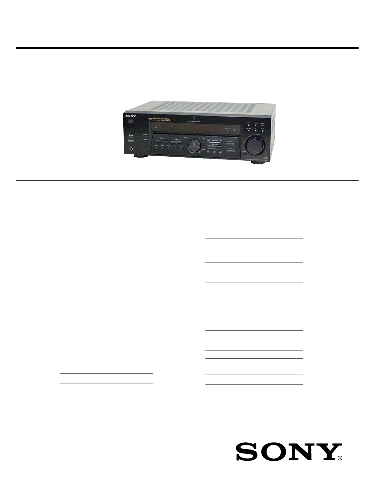
Sony STR-DE585 User manual

1
SERVICE MANUAL
Canadian Model
AEP Model
UK Model
STR-DE585
FM STEREO/FM-AM RECEIVER
AUDIO POWER SPECIFICATIONS
Amplifier section
POWER OUTPUT
Models of area code Canadian
Rated Power Output at Stereo Mode
(8 ohms 40 Hz – 20 kHz, THD 0.09 %)
100 W + 100 W
Reference Power Output
(8 ohms 1 kHz, THD 0.7 %)
FRONT 1) : 100 W/ch
CENTER1) : 100 W
SURR1) : 100 W/ch
Models of area code AEP, UK
Rated Power Output at Stereo Mode
(8 ohms 1 kHz, THD 0.7 %)
100 W + 100 W2)
Reference Power Output
(8 ohms 1 kHz, THD 0.7 %)
FRONT 1) : 100 W/ch
CENTER1) : 100 W
SURR1) : 100 W/ch
1) Depending on the sound field settings and the
source, there may be no sound output.
2) Measured under the following conditions:
Area code Power requirements
AEP, UK 230 V AC, 50 Hz
SPECIFICATIONS
Frequency response
MULTI CH IN, CD, 10 Hz – 50 kHz
MD/TAPE, DVD/LD, +0.5/–2 dB (with sound
VIDEO 1, 2 field, and tone bypassed)
Inputs (Analog)
MULTI CH IN, CD, Sensitivity: 250 mV
MD/TAPE, DVD/LD, Impedance: 50 kilohms
VIDEO 1, 2 S/N 3) : 96 dB
(A, 250 mV4) )
3) INPUT SHORT (with sound field and tone
bypassed).
4) Weighted network, input level.
Inputs (Digital)
DVD/LD (Coaxial) Sensitivity: –
Impedance: 75 ohms
S/N: 100 dB
(A, 20 kHz LPF)
VIDEO 2 (Optical) Sensitivity: –
Impedance: –
S/N: 100 dB
(A, 20 kHz LPF)
Outputs
MD/TAPE (REC Voltage: 250 mV
OUT), VIDEO1 Impedance: 10 kilohms
(AUDIO OUT)
SUB WOOFER Voltage: 2 V
Impedance: 1 kilohms
Tone
Gain levels: ±6 dB, 1 dB step
Ver 1.0 2002. 04
9-873-966-01
2002D0400-1
© 2002. 04
Sony Corporation
Home Audio Company
Published by Sony Engineering Corporation
Manufactured under license from Dolby Laboratories.
“Dolby”, “Pro Logic” and the double-D symbol are
trademarks of Dolby Laboratories.
“DTS” and “DTS Digital Surround” are registered
trademarks of Digital Theater Systems, Inc.
– Continued on next page –

2
STR-DE585
FM tuner section
Tuning range 87.5 - 108.0 MHz
Antenna terminals 75 ohms, unbalanced
Intermediate Frequency 10.7 MHz
Sensitivity
Mono: 18.3 dBf, 2.2 µV/75 ohms
Stereo: 38.3 dBf, 22.5 µV/75 ohms
Usable sensitivity 11.2 dBf, 1 µV/75 ohms
S/N
Mono: 76 dB
Stereo: 70 dB
Harmonic distortion at 1 kHz
Mono: 0.3%
Stereo: 0.5%
Separation 45 dB at 1 kHz
Frequency response 30 Hz – 15 kHz,
+0.5/–2 dB
Selectivity 60 dB at 400 kHz
AM tuner section
Tuning range
Models of area code Canadian
With 10-kHz tuning scale: 530 – 1710 kHz5)
With 9-kHz tuning scale: 531 – 1710 kHz5)
Models of area code AEP, UK
With 9-kHz tuning scale: 531 – 1602 kHz
Antenna Loop antenna
Intermediate Frequency 450 kHz
Usable sensitivity 50 dB/m (at 1,000 kHz or
999 kHz)
S/N 54 dB (at 50 mV/m)
Harmonic distortion 0.5 % (50 mV/m, 400 Hz)
Selectivity
At 9 kHz: 35 dB
At 10 kHz: 40 dB
5) You can change theAM tuning scale to 9 kHz or
10 kHz. After tuning in anyAM station, turn off
the receiver. Hold down PRESET TUNING + and
press ?/1 . All preset stations will be erased when
you change the tuning scale. To reset the scale to
10 kHz (or 9 kHz), repeat the procedure.
Video section
Inputs
Video: 1 Vp-p, 75 ohms
Outputs
Video: 1 Vp-p, 75 ohms
General
Power requirements
Area code Power requirements
Canadian 120 V AC, 60 Hz
AEP, UK 230 V AC, 50/60 Hz
Power consumption
Area code Power consumption
Canadian 300 VA
AEP, UK 180 W
Power consumption (during standby mode)
0.5 W
Dimensions 430 ×145 ×298 mm
(16 7/8 ×5 6/8 ×11 6/8 in.)
including projecting parts
and controls
Mass (Approx.) 7.0 kg (15 lb 7 oz)
Supplied accessories
FM wire antenna (1)
AM loop antenna (1)
•Models of area code Canadian
Remote commander RM-PP506 (1)
R6 (size-AA) batteries (2)
•Models of area code AEP, UK
Remote commander RM-U306 (1)
R6 (size-AA) batteries (2)
Design and specifications are subject to change
without notice.

3
STR-DE585
MODEL IDENTIFICATION
— BACK PANEL —
Part No.
Area code Part No.
Canadian 4-238-189-1s
AEP 4-240-192-0s
UK 4-240-192-1s
1.5 k
Ω
0.15 µFAC
voltmeter
(0.75 V)
To Exposed Metal
Parts on Set
Earth Ground
SAFETY CHECK-OUT
After correcting the original service problem, perform the follow-
ing safety check before releasing the set to the customer:
Checkthe antenna terminals,metal trim, “metallized” knobs,screws,
and all other exposed metal parts forAC leakage.
Check leakage as described below.
LEAKAGE TEST
The AC leakage from any exposed metal part to earth ground and
from all exposed metal parts to any exposed metal part having a
return to chassis, must not exceed 0.5 mA (500 microampers.).
Leakage current can be measured by any one of three methods.
1. A commercial leakage tester, such as the Simpson 229 or RCA
WT-540A. Follow the manufacturers’instructions to use these
instruments.
2. A battery-operated AC milliammeter. The Data Precision 245
digital multimeter is suitable for this job.
3. Measuring the voltage drop across a resistor by means of a
VOM or battery-operated AC voltmeter. The “limit” indica-
tion is 0.75 V, so analog meters must have an accurate low-
voltage scale. The Simpson 250 and Sanwa SH-63Trd are ex-
amples of a passive VOM that is suitable. Nearly all battery
operated digital multimeters that have a 2 V AC range are suit-
able. (See Fig. A)
SAFETY-RELATED COMPONENT WARNING!!
COMPONENTS IDENTIFIED BY MARK 0OR DOTTED LINE
WITH MARK 0ON THE SCHEMATIC DIAGRAMS AND IN
THE PARTS LIST ARE CRITICAL TO SAFE OPERATION.
REPLACE THESE COMPONENTS WITH SONY PARTS WHOSE
PART NUMBERS APPEAR AS SHOWN IN THIS MANUAL OR
IN SUPPLEMENTS PUBLISHED BY SONY.
ATTENTION AU COMPOSANT AYANT RAPPORT
À LA SÉCURITÉ!!
LES COMPOSANTS IDENTIFIÉS PAR UNE MARQUE 0SUR LES
DIAGRAMMESSCHÉMATIQUES ET LALISTE DES PIÈCESSONT
CRITIQUES POUR LA SÉCURITÉ DE FONCTIONNEMENT. NE
REMPLACER CES COMPOSANTS QUE PAR DES PIÈCES SONY
DONT LES NUMÉROS SONT DONNÉS DANS CE MANUEL OU
DANS LES SUPPLÉMENTS PUBLIÉS PAR SONY.

4
TABLE OF CONTENTS
1. GENERAL
Main unit ................................................................................. 5
Remote button description....................................................... 6
2. DISASSEMBLY
2-1. Case ..................................................................................... 8
2-2. Front Panel Section ............................................................. 9
2-3. Back Panel........................................................................... 9
2-4. Digital Board ..................................................................... 10
2-5. Standby Board ................................................................... 10
2-6. Main Board ....................................................................... 11
3.TEST MODE...................................................................... 12
4. DIAGRAMS
4-1. IC Pin Descriptions ........................................................... 13
4-2. Block Diagram – Tuner/Audio Section – .......................... 16
4-3. Block Diagram – Digital Section – ................................... 17
4-4. Block Diagram – Video/Display Section – ....................... 18
4-5. Block Diagram – Power Section – ....................................19
4-6. Circuit Boards Location .................................................... 20
4-7. Printed Wiring Boards – Main Section – .......................... 21
4-8. Schematic Diagram – Main Section (1/2) – ...................... 22
4-9. Schematic Diagram – Main Section (2/2) – ...................... 23
4-10. Printed Wiring Board – Digital Section (1/2) – ................ 24
4-11. Printed Wiring Board – Digital Section (2/2) – ................ 25
4-12. Schematic Diagram – Digital Section (1/2) – ................... 26
4-13. Schematic Diagram – Digital Section (2/2) – ................... 27
4-14. Printed Wiring Board – Video Section – ........................... 28
4-15. Schematic Diagram – Video Section –.............................. 29
4-16. Printed Wiring Boards – Display Section – ...................... 30
4-17. Schematic Diagram – Display Section –........................... 31
4-18. Printed Wiring Board – Power Section – .......................... 32
4-19. Schematic Diagram – Power Section – ............................. 33
4-20. IC Block Diagrams............................................................ 34
5. EXPLODEDVIEWS
5-1. Case Section ...................................................................... 35
5-2. Front Panel Section ........................................................... 36
5-3. Chassis Section-1 .............................................................. 37
5-4. Chassis Section-2 .............................................................. 38
6. ELECTRICAL PARTS LIST......................................... 39
STR-DE585

5
STR-DE585
SECTION 1
GENERAL This section is extracted
from instruction manual.
List of Button Locations and Reference Pages
5
GB
wdwfwhwjwkwlesedefegehek ej e;ea wg
1 7 84 qs0qa523 6qf qg qjqh qkqlw;qd waws9
List of Button Locations and Reference Pages
Main unit
How to use this page
Use this page to find the location of buttons
that are mentioned in the text.
FM MODE (Models of area code
CEL, CEK only) ed, (Except for
models of area code CEL, CEK)
ef (31)
INPUT MODE qg (21)
IR (receptor) 4(38, 45, 51)
LEVEL 0(20, 27, 55)
M
MASTER VOLUME wd (20, 49)
MD/TAPE qj (21)
MEMORY eh (30, 32)
MENU +/– e; (16, 27, 35, 36)
MENU </> ea (16, 27, 35, 36)
MODE wj (24, 50)
MULTI CHANNEL DECODING
(indicator) (Except for
STR-DE485E) 7(21)
MULTI CH IN (Except for
STR-DE485E) qf (21)
MUTING wf (21, 49)
N —S
NAME 8(35)
PHONES (jack) ek (21)
PRESET/PTY SELECT +/–
(Models of area code CEL, CEK
only) 3(32, 33)
PRESET TUNING +/– (Except
for models of area code CEL,
CEK) 3(32, 53)
PTY (Models of area code CEL,
CEK only) ef (33)
SET UP 6(4, 16, 36, 54)
SHIFT eg (32)
SLEEP (STR-DE485E only)qf
(36)
SURR qd (27, 54)
T —Z
TREBLE +/– qh (29, 54)
TUNER ws (21, 30-32, 35)
TUNING +/– 5(31)
VIDEO 1 qk (21)
VIDEO 2 w; (21)
BUTTON DESCRIPTIONS
`/1 (power) 1(4, 15, 20, 29,
30, 53)
ALPHABETICAL ORDER
0 —9
2 CH wh (25)
A —D
A.DEC wk (23–25)
AM (Except for models of area
code CEL, CEK) es (30, 31)
BASS +/– wg (29, 54)
CD ql (21)
CINEMA STUDIO EX A, B, C
9(23, 24)
Digital Cinema Sound (indicator)
qs (23)
DIMMER ej (22)
DISPLAY 2(22, 33, 51)
Display qa (22)
DVD/LD wa (21)
E —L
ENTER wl (35)
FM (Except for models of area
code CEL, CEK) ed (30, 31)
FM/AM (Models of area code
CEL, CEK only) es (30, 31)
Illustration number
r
NAME 8(35)
R R
Name of button/part Reference page

6
STR-DE585
39
GB
38
GB
You can use the remote RM-PP506 to operate
the components in your system.
Operations Using the Remote RM-PP506
The tables below show the settings of each
button.
Remote Operations Function
Button
SLEEP Receiver Activates the sleep
function and the duration
which the receiver turns
off automatically.
?/1 Receiver
Turns the receiver on or off.
>10
1
4
7
2
5
8
3
6
9
0
MONITOR 2ND ROOM
VIDEO 1 VIDEO 2 VIDEO 3 DVD/LD TV/SAT
AUX
TV/VIDEO
INPUT MODE
CLEAR
– SUB CH +
– VOL +
POSITION SWAP
SEARCH
MODE AUDIO
SPLIT
ENTER ANT
TV/VTR
D. SKIP/
CH/PRESET
MD/TAPE CD/SACD TUNER PHONO
SHIFT DISC
JUMP
AUTO DEC
AV
DISPLAY TEST
TONE NIGHT
MODE
ON
SCREEN
MAIN
MENU
EXIT/
RETURN
AV
MENU
TITLE/
GUIDE
ENTER/
EXEC
MULTI/2CH
A. DIRECT
EQ/
TONE
MUTING
MUTING
MODE 2CH PRESET
P IN P
– /– –
SOUND FIELD
D.TUNING
AV1 AV2 3RD
(SOURCE)
WIDE
/11 /10 /12
SLEEP
? / 1
SYSTEM
STANDBY
MASTER
VOL
.Mm
nNX
>
x
AV
? / 1
Remote Operations Function
Button
VIDEO 1 Receiver To watch VCR.
(VTR mode 3)
VIDEO 2 Receiver To watch VCR.
(VTR mode 1)
VIDEO 3 Receiver To watch VCR.
(VTR mode 2)
DVD/LD Receiver To watch DVD or laser
disc.
TV/SAT Receiver To watch TV programs
or satellite receiver.
AUXReceiver To listen to an audio
equipment.
MD/TAPE Receiver To listen to Minidisc
or audio tape.
CD/SACD Receiver To listen to compact disc.
TUNER Receiver To listen to radio
programs.
PHONO Receiver To listen to turntable.
INPUT Receiver Selects input mode for
MODE your digital components.
AUDIO Receiver To assign the audio input
SPLIT for each function.
SHIFT Receiver Press repeatedly to select
a memory page for
presetting radio stations
or tuning to preset
stations.
D.TUNING Receiver Tuner station direct key-
in-mode.
AUTO DEC
Receiver Selects AUTO
DECODING mode.
MODE +/– Receiver Selects sound field mode.
2CH Receiver Selects 2CH mode.
PRESET Receiver Selects preset sound field
(e.g. Cinema Studio
EX A, B, C)
TEST Receiver Press to output test tone.
TONE

7
STR-DE585
Operations Using the Remote RM-U306
45
GB
Except for STR-DE585 area code CA
You can use the remote RM-U306 to operate
the components in your system.
Remote button
description
NX
mM
.>
12 3
45 6
78
0
9
MD/TAPE CD TUNER
TV/VIDEO
VIDEO 2
VIDEO 1 DVD/LD
SYSTEM
STANDBY
>10
SHIFT
CH/PRESET
-
ANT
TV/VTR
SOUND FIELD
–+
MASTER
VOL
TEST TONE MAIN MENU MULTI CH
ENTER
D.SKIP
A.DEC 2CH
MODE
D.TUNING
TOP MENU DVD MENU
ENTER
RETURN
f
F
Gg
SLEEP AV
?/1 ?/1
MENU
TV VOL TV CH
MUTING
O
x
Operations Using the Remote RM-U306
continued
The tables below show the settings of each
button.
Remote Operations Function
Button
SLEEP Receiver Activates the sleep
function and the duration
which the receiver turns
off automatically.
?/1 Receiver Turns the receiver on or
off.
46
GB
Remote button description
(continued)
Remote Operations Function
Button
VIDEO 1 Receiver To watch VCR.
(VTR mode 3)
VIDEO 2 Receiver To watch VCR.
(VTR mode 1)
DVD/LD Receiver To watch DVD or laser
disc.
MD/TAPE Receiver To listen to Minidisc or
audio tape.
CD Receiver To listen to compact disc.
TUNER Receiver To listen to radio
programs.
SHIFT Receiver Press repeatedly to select
a memory page for
presetting radio stations
or tuning to preset
stations.
D.TUNING
Receiver Tuner station direct key-
in-mode.
A.DEC Receiver Select AUTO DECODE
mode.
MODE Receiver Selects sound field mode.
2CH Receiver Selects 2CH mode.
TEST Receiver Press to output test tone.
TONE
MAIN Receiver Press this button
MENU repeatedly to select one
of the four cursor modes:
SURR, LEVEL, SET UP
and NAME.
MULTI CH
Receiver Selects MULTI CH IN
source.
MENU </> Receiver Selects a menu item.
MENU +/– Receiver Makes adjustment or
change the setting.
MUTING Receiver Mutes the sound from the
receiver.

8
STR-DE585
Note : This set can be disassemble according to the following sequence.
SECTION 2
DISASSEMBLY
2-1. CASE
2-1. CASE
(Page 8)
2-2. FRONT PANEL SECTION
(Page 9) 2-3. BACK PANEL
(Page 9)
SET
2-4. DIGITAL BOARD
(Page 10)
2-5. STANDBY BOARD
(Page 10)
2-6. MAIN BOARD
(Page 11)
Note : Follow the disassembly procedure in the numerical order given.
1
two screws
(case 3 TP2)
2
two screws
(case 3 TP2)
3
two screws
(case 3 TP2)
4
cas
e

9
STR-DE585
2-2. FRONT PANEL SECTION
2-3. BACK PANEL
5
front panel section
3
two screws
(BVTP3 x 8)
1
CNS4
2
CNP791
4
four screws
(BVTP3 x 8)
1
CNS7
2
CNS8
3
CNP901
4
CNP154
5
two screws
(BVTP3 x 8)
8
two screws
(BVTP3 x 8)
7
two screws
(BVTP3 x 8)
6
five screws
(BVTP3 x 8
)
9
screw (BVTP3 x 8)
0
screw (BVTP3 x 8)
qa
screw (BVTP3 x 8)
qs
screw
(BVTP3 x 8)
qd
back panel (DE4)(Canadian)
back panel (DE5)(AEP, UK)

10
STR-DE585
2-4. DIGITAL BOARD
1
CNS4
5
CNS1
6
CNS2
2
CNP6
3
CNP5
8
screw (BVTP3 x 8)
9
bracket (digital)
7
DIGITAL board
4
screw (BVTP3 x 8
)
5
STANDBY board
1
CNP915
2
CNP902
3
CNP903
4
three screws
(BVTP3 x 8)
2-5. STANDBY BOARD

11
STR-DE585
7
MAIN board
1
CNP801
2
CNP802
5
screw
(BVTP3 x 8)
3
two screws
(BVTP3 x 6)
4
two screws
(BVTP3 x 6)
6
two screws
(BVTP3 x 8
)
2-6. MAIN BOARD

12
STR-DE585
SOFTWARE VERSION DISPLAY MODE
*The software version is displayed.
*Procedure:
While depressing the [ENTER] and the SOUND FIELD [A.DEC]
buttons simultaneously, press the power ?/1 button to turn on
the main power. The model name, destination and the software
version are displayed.
FLUORESCENT INDICATORTUBETEST MODE
*All fluorescent segments are tested. When this test is activated,
all segments turn on at the same time, then each segment turns
on one after another.
*Procedure:
While depressing the [MD/TAPE] and the [SHIFT] buttons simul-
taneously, press the power ?/1 button to turn on the main power.
1. All segments turn on.
[MULTI CHANNEL DECODING], [Digital Cinema Sound],SOUND
FIELD [A.DEC], [MODE], [2CH] and [SET UP] LED turn on.
2. Press the [VIDEO 1] button, confirm display
SOUNDFIELD [A.DEC],[MODE],SOUND CONTROL[LEVEL],
[SET UP] and [Digital Cinema Sound] LED turn on.
3. Press the [VIDEO 1] button, confirm display
[MULTI CHANNEL DECODING],SOUNDFIELD [2CH],SOUND
CONTROL [SURR] and [NAME] LED turn on.
4. Press the [VIDEO 1] button, All segments turn off.
5. Every pressing of the [VIDEO 1] button turns on each segment
and LED one after another in the same order.
(Not only the [VIDEO 1] button, but also the other buttons such
as[VIDEO 2],[DVD/LD], [MD/TAPE], [CD],[TUNER] can be used.)
SECTION 3
TEST MODE
SW
L
SL
CR
SSR
SLEEP
SP.OFF
( ( ( L F E ) ) )
DIGITAL
OPT COAX MULTI CH IN
PRO LOGIC DTS MPEGSTEREO MONO RDS MEMORY
MUTINGINFONEWSTAEQD.RANGE
D
D
dB
kHz
mft.
MHz
SW
LR
S
SLEEP
L F E
COAX
PRO LOGIC MPEGSTEREO RDS
MUTINGINFOTAD.RANGE
D
D
k
m
MHz
SL
C
SR
SP.OFF
( ( ( ) ) )
DIGITAL
OPT MULTI CH IN
DTS MONO MEMORY
NEWSEQ
dB
Hz
ft.
FACTORY PRESET MODE
*All preset contents are reset to the default setting.
*Procedure:
While depressing the [VIDEO 1] and the SOUND FIELD [2CH]
buttons simultaneously, press the power ?/1 button to turn on
the main power. The message FACTORY appears and switch
off the set.
While depressing the [VIDEO 1] and the SOUND FIELD [2CH]
buttons simultaneously, press the power ?/1 button again. The
message FACTORY appears and the preset contents are reset to
the default values.
SOUND FIELD CLEAR MODE
*The preset sound field is cleared when this mode is activated.
Use this mode before returning the product to clients upon
completion of repair.
*Procedure:
While depressing the SOUND FIELD [MODE] button, press the
power ?/1 button to turn on the main power. The message S. F.
CLR appears and initialization is performed.
AM CHANNEL STEP 9 kHz/10 kHz
SELECTION MODE
*Either the 9 kHz step or 10 kHz step can be selected for theAM
channel step.
*Procedure:
Set the [TUNER] to [AM]. Turn off the main power.
While depressing the [TUNING+] button or the
[PRESET TUNING ] button, press the power ?/1 button to turn
on the main power. Either the message 9 k STEP or 10 k STEP
appears. Select the desired step.
*For Canadian model only
KEY CHECK MODE
*Button check
*Procedure:
While depressing the [VIDEO 1] and the [SHIFT] buttons simul-
taneously, press the power ?/1 button to turn on the main power.
“REST 39” appears.
Every pressing of any button other than the ?/1 , [TREBLE+, ]
and the [BASS+, ] counts down the buttons. The buttons which
are already counted once are not counted again. When all but-
tons are pressed “REST 04” appears.
When [MASTER VOLUME] is rotated in clockwise direction, “VOL
MIN”, “VOL 1” to “VOL 73”, “VOL MAX” appear.

13
STR-DE585
SECTION 4
DIAGRAMS
1VSS — Ground
2XRST I Reset signal input
3EXTIN I Not used (connected to ground)
4FS2 I Not used (connected to ground)
5VDDI I Power supply
6FS1 I Not used (connected to ground)
7PLOCK O Internal PLL lock signal output (Not used (open))
8VSS — Ground
9MCLK1 I Clock signal input (13.5 MHz)
10 VDDI I Power supply
11 VSS — Ground
12 MCLK2 O Clock signal output (13.5 MHz)
13 MS I Switching of master/slave operation (L : internal clock, H : EXTIN clock is used)
14 SCKOUT O Internal system clock signal output
15 LRCKI1 I Not used (open)
16 VDDE I Power supply
17 BCKI1 I Not used (open)
18 SDI1 I Audio IF data input
19 LRCKO O Sampling clock output for digital audio serial data
20 BCKO O Bit clock output terminal for digital audio serial data
21 VSS — Ground
22 KFSIO I/O Audio clock signal (364fs/256fs) input/output
23 to 25 SDO1 to SDO3 O Digital audio serial data output
26 SDO4 O Audio IF serial output (Not used (open))
27 SPDIF O Not used (open)
28 LRCKI2 I Sampling clock input for audio serial data
29 BCKI2 I Bit clock input terminal for audio serial data
30 SDI2 I Digital audio data input
31 VSS — Ground
32 HACN O Acknowledge signal output for system control
33 HDIN I Serial data input for system control
34 HCLK I Clock input for system control
35 HDOUT O Serial data output for system control
36 HCS I Chip select input for system control
37 SDCLK O Not used (open)
38 CLKEN O Not used (open)
39 RAS O Not used (open)
40 VDDI I Power supply
41 VSS — Ground
42 CAS O Not used (open)
43 DQM/OE0 O Not used (open)
44 CS0 O External memory chip select (SRAM)
45 WE0 O SRAM write enable output
46 VDDE I Power supply
47 WMD1 I Not used (connected to “H”)
48 VSS — Ground
49 WIMD0 I Not used (connected to “H”)
50 PAGE2 O Not used (open)
51 VSS — Ground
52 PAGE1 O External memory page switching signal output (Not used (open))
53 PAGE0 O External memory page switching signal output (Not used (open))
4-1. IC PIN DESCRIPTIONS
• IC1201 CXD9617R (DSP) (DIGITAL Board (1/2))
Pin No. Pin Name I/O Description

14
STR-DE585
54 BOOT I Not used (connected to ground)
55 BTACT O Not used (open)
56 BST I Boot stop signal input
57 MOD1 I Operation mode signal input (L : 386fs, H : 256fs)
58 MOD0 I Operation mode signal input (L : single chip mode, H : use prohibited)
59 EXLOCK I Lock signal input
60 VDDI I Power supply
61 VSS — Ground
62, 63 A17, A16 O Not used (open)
64 to 66 A15 to A13 O External memory address output (SRAM)
67 GP10 O LRCK0
68 GP9 (DECODE) O DECODE
69 GP8 (AUDIO) I AUDIO
70 VDDI I Power supply
71 VSS — Ground
72 to 75 D15/GP7 to D12/GP4 I/O External memory data input/output (general port)
76 VDDE I Power supply
77 to 80 D11/GP3 to D8/GP0 I/O External memory data input/output (general port)
81 VSS — Ground
82 to 85 A9 to A12 O External memory address output (SRAM)
86 TDO O Not used (open)
87 TMS I Not used (open)
88 XTRST I Not used (open)
89 TCK I Not used (open)
90 TDI I Not used (open)
91 VSS — Ground
92 to 97 A8 to A3 O External memory address output (SRAM)
98, 99 D7, D6 I/O External memory data input/output (SRAM)
100 VDDI I Power supply
101 VSS — Ground
102 to 105 D5 to D2 I/O External memory data input/output (SRAM)
106 VDDE I Power supply
107, 108 D1, D0 I/O External memory data input/output (SRAM)
109, 110 A2, A1 O External memory address output (SRAM)
111 VSS — Ground
112 A0 O External memory address output (SRAM)
113 PM I PLL initialization input terminal
114, 115 SDI3, SDI4 I Not used (open)
116 SYNC I Sync/async selection input (L : sync, H : async)
117 to 119 VSS — Ground
120 VDDI I Power supply
Pin No. Pin Name I/O Description

STR-DE585
15 15
Pin No. Pin Name I/O Description
1DATAO I Serial data input for DIR
2GP9 I Decode signal input
3BST O Boot stop signal output to DSP
4 HCS O Chip select signal output to DSP
5HACNIAcknowledge signal input for DSP
6XRST O Reset signal output to DSP
7PMOPLL initialization output to DSP
8PDOPower down signal output to CODEC
9 SMUTE O Soft mute signal output to CODEC
10 CDT1 O Control data output to CODEC
11 VSS — Ground
12 SCL O Serial data clock to CODEC
13 CS O Chip select signal output to CODEC
14 DATA O Serial data output to VOL/TUNER
15 CLK O Clock signal output to VOL/TUNER
16 LATCH-VOL IC O Latch signal output toVOL/TUNER
17 SPK B RELAY O Speaker out control signal output (Fixed at “L”)
18 HDOUT I Serial data for DSP
19 HDIN O Serial data to DSP
20 HCLK O Clock signal output to DSP
21 F.MUTE O Function input mute signal output
22 AC MUTE O Power amp mute signal output
23 VCC5 I Power supply
24 ANA/DIG I Muting and error port signal input
25 HP DETECT I Headphone detect signal input
26 DCS LED O LED (Digital Cinema Sound) driver signal output
27 FLASH2 O Flash programming signal output
28 SP SWITCH/FLASH1 I/O Speaker ON/OFF signal output
29 MCH LED O LED (MULTI CHANNEL DECODING) driver signal output
30 MODE O LED (MODE) driver signal output
31 2CH O LED (2CH) driver signal output
32 AFD O LED (A.F.D.) driver signal output
33 SCL O Clock signal output to EEPROM
34 SDA I/O Serial data to EEPROM
35 AVCC I Power supply
36 AVRH I Not used (connected to “H”)
37 AVSS — Ground
38 to 41 A/D0 to A/D3 I Key signal input (A/D port)
42 VSS — Ground
43 RDS SIGNAL I RDS signal input (AEP, UK model)
44 MODEL I Model detection port
45 VERSION I Version resistor port
46 NC O Not used (Fixed at “L”)
47 NC O Not used (Fixed at “H”)
48 STOP I Input signal when AC off
49 MD0 — Selection of micom operation mode
50 MD1 — Not used (connected to “H”)
51 MD2 — Selection of micom operation mode
52 RDS CLOCK I RDS clock signal output (AEP, UK model)
53 RDS DATA I RDS data output (AEP, UK model)
54 SIRCS I Input data from remote control receiver
55 FUSE DETECT I Power down detect input
• IC1601 MB90478PF-G-120-BND (SYSTEM CONTROL) (DIGITAL Board (2/2))
Pin No. Pin Name I/O Description
56 POWER KEY I Detect power switch key
57 JOG (B) I Jog encoder signal input (Fixed at “L”)
58 JOG (A) I Jog encoder signal input (Fixed at “L”)
59 VOL (B) I Volume encoder signal input
60 VOL (A) I Volume encoder signal input
61 DIN O Serial data output to FL driver
62 CLK O Clock signal output to FL driver
63 FL_STB O Strobe signal output to FL driver
64 CONTROLA1 OUT O Control A1 signal output (Fixed at “L”)
65 CONTROLA1 IN I Control A1 signal input (Not used)
66 POWER RELAY O Control power relay driver output
67 PROTECTOR I Detect protector status input
68 HEADPHONE RELAY O Control headphone relay driver output
69 WOOFER RELAY O Control woofer speaker relay driver output
70 REAR RELAY O Control rear speaker relay driver output
71 CENTER RELAY O Control center speaker relay driver output
72 PREOUT/FRONT RELAY O Control front speaker relay driver output
73 TUNED O Tuned signal output to tuner
74 STEREO O Stereo signal output to tuner
75 MUTE O Mute signal output to tuner
76 DO I Serial data input for tuner
77 RSTX I Reset signal input
78 SLATCH O Latch signal to tuner
79 X1A — Not used (open)
80 X0A — Not used (connected to ground)
81 VSS — Ground
82 X0 I Clock signal input (16 MHz)
83 X1 O Clock signal output (16 MHz)
84 VCC3 I Power supply
85 NC I Not used (Fixed at “L”)
86 NC O Not used (Fixed at “L”)
87 to 90 SW4 to SW1 O Video input select signal output
91 SELECT1 O Optical input select signal output (Fixed at “L”)
92 SELECT2 O Optical input select signal output (Fixed at “L”)
93 XMODE O Mode signal output to DIR
94 CKSEL1 O Clock select signal output to DIR
95 CLK O Clock signal output to DIR
96 CE O Chip select signal output to DIR
97 DI O Serial data output to DIR
98 DO I Serial data input for DIR
99 ERROR I Error signal input for DIR
100 XSTATE I XSTATE signal input for DIR

STR-DE585
1616
4-2. BLOCK DIAGRAM — TUNER/AUDIO SECTION —
1
2
67
R-CH
R-CH
R-CH
J402 (1/2)
J403
J404 (1/2)
J401
-1
L
-2
R
INCD
DVD/LD
MD/TAPE
AUDIO
IN
FM 75Ω
COAXIAL
AM
ANTENNA
TU+10V
TM301
FM/AM TUNER UNIT
TU+3.3V
+10V
L CH
R CH
STEREO
TUNED
MUTE
CE
RDS SIGNAL
RDS DATA
RDS CLOCK
STEREO
TUNED
MUTE
SLATCH
DO
FM OUT
RDS DATA
RDS INT
STEREO
TUNED
MUTE
CE CLK
DATA
DO/DI
DATA
CLK
LATCH VOL IC
WOOFER RELAY
ST-DO/MC-DI
ST-DI/MC-DO
CLK
AEP,UK MODEL
STEREO
TUNED
MUTE
CE
DO/DI
DATA
CLK
FM SIGNAL OUT
RDS DATA
FM OUT
RDS DATA
RDS INT
RDS INT
R-CH
LREC 3
61
LREC 1
10
ALOUT
9
AROUT
R-CH
IN 8
IN 9
IN 5
IN 6
IN 7
IN 8
IN 1
IN 2
IN 3
AL IN
ASL IN
ASW IN
AC IN
3IN 10
69
68
70
71
R-CH
R-CH
VIDEO 1
VIDEO 2
AUDIO
IN
AUDIO
IN
62
63
64
R-CH
R-CH
MULTI
CH IN
FRONT
SURROUND
CENTER
SUB
WOOFER
13
16
29
43
53
52
76
73
75
78
76
14
15
16
69
32
31
27
49
LSELOUT
45
SLDELOUT
50
46
37
CSELOUT 38
51
LOUT
47
39
33
SWSELOUT 34 35 5 7
SLOUT
55
ROUT
R-CH
R-CH 43
SROUT
COUT
SWOUT
20
21
22
R-CH
R-CH
R-IN
L-IN
J402 (2/2)
-4
R
-3
L
OUT MD/TAPE
VIDEO 1
J404 (2/2)
-3
L
-4
R
AUDIO
OUT
-1
L
-2
R
-5
L
-6
R
-1
L
-2
R
-1
L
-2
R
-3
L
-4
R
IN
-3
L
-4
R
15
MUTE
Q361,362
MUTE
Q365,366
MUTE
Q363
MUTE
Q364
RELAY
DRIVER
Q560
DSLIN
DSWIN
DCIN
DLIN
DSL IN
DSW IN
DC IN
DL IN
MCU
I/F
DATA
CLK
LATCH
DIR
FUNCTION
SELECT
IC201
RY560
Q379
INV.
FC MUTE
J405
SUB
WOOFER
AUDIO
OUT
FL-CH
FR-CH
SL-CH
SR-CH
C-CH
WOOFER
AMP
IC401
11
0/6/12dB
0/6/12dB
0/6/12dB
0/6/12dB
0/6/12dB
ATT
0/-6dB
+3.3V
REG
Q471
+7V
VCC
+3.3V
+7V
-6
-5
TUNER
VOL IC/
TUNER
SYSTEM
CONTROL
IC1601 (1/4)
POWER
SECTION
4
DIGITAL
SECTION
1
DIGITAL
SECTION
2
DIGITAL
SECTION
3
• Signal path
: TUNER (FM/AM)
: CD (ANALOG)
: VIDEO
• R-ch is omitted due to
same as L-ch.
(Page 17)
(Page 17)
(Page 17)
(Page 19)

STR-DE585
17 17
4-3. BLOCK DIAGRAM — DIGITAL SECTION —
30
+5V-2
AVDD
AMP
IC1502
DSI1 SDTI1 LOUT1
LOUT 3
ROUT 3
LOUT 2
SD01
SDTO
29
9 18
GP8
AUDIO 24 69
KFSI0
CKOUT 13 22
BCKI2
BCK 14 29
LRCKI2
LRCK 15 28
DSI2
CS
WE
DATAO
SCKOUTMCLKI 39 14
23 6
SDTI2
SD02 24 7
SDTI3
SD03 25 8
27
GP10 67
LRCK
LRCKO 19 5
BCK
BCKO 20 4
17
X1201
13.5MHz
X1101
12.288MHz
MCLK1 9
MCLK2 12
CSO 44
WEO 45
68 56
108,107,105 -102,99,
98,79 - 77,75 - 72
24 - 27,42 - 44,
1 - 5,18 - 21
29 - 32,35 - 38,
16-13,10 - 7
112,110,109,99 - 92,
85-82,66 - 64
6
17
211336 35 33 3432
321 6 74 18 19 205
EXLOCK
ERROR
21
22
21
99
1
95 96 97 98 94 100
38 37 36 35 33 47 17
3 43 42 41
8 9 10 12 13
DAC
DAC
DAC
DAC
23
24
25
AUDIO
I/F
(2/2)
INPUT DATA
DEMODULATOR
Pa,Pb DETECTION LOCK
DETECTION
MICROPROCESSOR
I/F
C bit DETECTION 34 59
16 30
DVD/LD
IN
DIGITAL
COAXIAL
VIDEO 2
IN
OPTICAL
OUT
IC1105
IC1102
DIR
IC1101
J1101
23 WAVE
SHAPER
6 7 2 1
+5V-1
D5V
+2.5V
VDDI
+3.3V
VDDE
+3.3V
VDD NC
L-IN
R-IN
FC MUTE
R-CH
L IN-
L IN+ LPF
AUDIO
I/F
(1/2)
CODEC
IC1501
DSP
IC1201
ROM
IC1202
DLIN
DCIN
DSWIN
DSLIN
PD
S.MUTE
CDT1
CCLK
CS
PD
SMUTE
CDT1
SCL
CS
CODEC
GP9
DATAO
HACN
BST
HCS
XRST
HDIN
PM
HDOUT
HCLK
GP9
HACN
BST
HCS
XRST
HDIN
PM
HDOUT
HCLK
DSP
CLK
CE
DI
DO
CKSEL1
XSTATE
CLK
CE
DI
DO
BPSYNC
CKSEL1
XSTATE
DIR
5
4
XOUT
XIN
F.MUTE
Q1601
INV.
ERROR
Q1602
D1101
D0-15A0-15
D0-15A0-15
SYSTEM
CONTROL
IC1601 (2/4)
TUNER/
AUDIO
SECTION
3
TUNER/
AUDIO
SECTION
2
TUNER/
AUDIO
SECTION
1
ADC
• Signal path
: TUNER (FM/AM)
: CD (ANALOG)
: CD (DIGITAL)
• R-ch is omitted due to
same as L-ch.
(Page 16)
(Page 16)
(Page 16)

STR-DE585
1818
4-4. BLOCK DIAGRAM — VIDEO/DISPLAY SECTION —
13
1
15
5
3
4 610 14
88
83 61 7
14 - 29 42 - 31
82
34
33
5
6
8789 90
2
16
8
62 8
63
29
32
31
30
26
60
59
54
38
9
1
2
3
SW NETWORK S100-109
39 SW NETWORK S110-119
40 SW NETWORK S120-128
41 SW NETWORK S130-137,
S143,144
RV102
MASTER
VOLUME
LED
DRIVERS
Q100-104
56
28
27
51
49
77
23
13
VIDEO
IN
VIDEO 1
VIDEO
OUT MONITOR
VIDEO
OUT VIDEO 1
VIDEO
IN
VIDEO 2
VIDEO
IN
DVD/LD
+3.3V
(STBY)
RESET
IC1602
M.OUT
V1.OUT
VCC
V1
V2
DVD
X1
X0
SW3
SW2
SW4
SW1
SDA
EEPROM
VIDEO SW
SCL
POWER KEY
SP SWITCH/FLASH1
FLASH2
MD2
MD0
RSTX
VEE
IC807
IC804
+5V
REG
-5V
REG
+V
-V
J201 (2/2)
J200 (2/2)
FL101
FLUORESCENT
INDICATOR
TUBE
F1
F2
DIN
CLK
STB
SW1
SW2
SW3
VIDEO SELECTOR
IC103
SW3
SW2
SW4
SW1
SW5
D203,
D204
J201 (1/2)
J200 (1/2)
SDA
SCL
EEPROM
IC1604
X1601
20MHz
DIN
FL DRV/
LED DRV
BUFFER
IC101
CLK
FL_STB
MCH LED
AFD
2CH
MODE
DSC LED
SIRCS
VOL(A)
VOL(B)
A/D0
A/D1
A/D2
A/D3
5
4
2
1
10
9
6
3
8
1
3
FL DISPLAY
DRIVER
IC100
SEG1-16 GRID1-16
Q109
Q111
Q110
LED DRIVER
Q108
LED DRIVER
Q107
LED
MATRIX
D110-114
D100,
D102-104
1
REMOTE
CONTROL
RECEIVER
IC102
OUT
SIRCS
+5V-1
SYSTEM
CONTROL
IC1601 (3/4)
CNS3
FLASH1
FLASH2
MD2
MD0
RESET
1
2
7
6
5
FLASH
PROGRAMMING
S145
AFD-LED
MCH-LED
MODE-LED
DSC-LED
2CH-LED
12
I
/ I
OR
• Signal path
: VIDEO

STR-DE585
19 19
4-5. BLOCK DIAGRAM — POWER SECTION —
812
11
DRIVE POWER AMP
Q701-704
CURRENT
DETECT
Q705,706 RY791
RY701
RY601
PRE DRIVER
IC701
IN 2 +VOUT2
-VOUT2
SPEAKERS
IMPEDANCE
USE 8-16Ω
R
L
FRONT
L
SURROUND
CENTER
R
R-CH
R-CH
R-CH
FL-CH
FR-CH
SL-CH
C-CH
R-CH
SR-CH R-CH
TUNER/
AUDIO
SECTION
4
RY901
D804
F1
F2
-30V
+3.3V
(STBY)
+2.5V
+5V-1
-7V
+7V
TU+10V
TU+3.3V
-30V
F901
RECT
D910-913
T902
POWER
TRANSFORMER
D914
Q921 D915
D731
D734
D733
~
AC IN
OVERLOAD
DETECT
D740,Q740
1
67
6
5
DRIVE POWER AMP
Q501-504
CURRENT
DETECT
Q505,506
-30V REG
Q801
RELAY
DRIVER
Q901
PRE DRIVER
IC501
IN+ +VOUT
-VOUT
OVERLOAD
DETECT
D540,Q540
DOUBLER
COMMUTATION
812
11
DRIVE POWER AMP
Q651-654
CURRENT
DETECT
Q655,656
PRE DRIVER
IC702
IN 2 +VOUT2
-VOUT2
OVERLOAD
DETECT
D640,Q640
RELAY
DRIVER
Q790
RELAY
DRIVER
Q710
RELAY
DRIVER
Q610
RY501
RELAY
DRIVER
Q550
70
72
68
PROTECTOR
D721,722
Q722,723,725
25
66
48
71
OVERLOAD
DETECT AMP 72
IC601
Q692
Q691
+B
-B
-BB
+3.3V
REG 13
IC1905
BACK-UP
SWITCH 4
5
+3.3V 2
IC1901
+5V-2 +5V
REG 13
IC1503
+10V
REG 13
IC1902
-V
+V
+7V
REG 13
IC801
-7V
REG 23
IC802
+5V
REG 13
IC1903
+3.3V
REG 13
IC1904
R-CH
R-CH
R-CH
-BB +B
-BB +B
-BB +B
R-CH
R-CH R-CH
RECT
D802
RECT
D820-822
RECT
D902-905
T901
POWER
TRANSFORMER
D898,899
TM601
TM602
J791
PHONES
HP-RY
FRONT-RY
REAR-RY
CENTER-RY
HP DETECT
HP-RY
HP DETECT
FRONT-RY
REAR-RY
CENTER-RY
HEADPHONE
RELAY
PREOUT/FRONT
RELAY
REAR RELAY
PROTECTOR
HP DETECT
POWER RELAY
STOP
CENTER RELAY AEP,UK M0DEL
SYSTEM
CONTROL
IC1601 (4/4)
PRE
DRIVE
PRE
DRIVE
PRE
DRIVE
-B +B
-B +B
-B +B
• Signal path
: TUNER (FM/AM)
• R-ch is omitted due to
same as L-ch.
(Page 16)

STR-DE585
2020
THIS NOTE IS COMMON FOR PRINTEDWIRING
BOARDS AND SCHEMATIC DIAGRAMS.
(In addition to this, the necessary note is
printed in each block.)
for schematic diagram:
•All capacitors are in µF unless otherwise noted. pF: µµF
50 WV or less are not indicated except for electrolytics
and tantalums.
•All resistors are in Ωand 1/4W or less unless otherwise
specified.
•f: internal component.
•2: nonflammable resistor.
•5: fusible resistor.
•C: panel designation.
•A: B+ Line.
•B: B– Line.
•Voltage and waveforms are dc with respect to ground
under no-signal (detuned) conditions.
no mark : FM
•Voltagesaretaken with aVOM(Input impedance10MΩ).
Voltage variations may be noted due to normal produc-
tion tolerances.
•Waveforms are taken with a oscilloscope.
Voltage variations may be noted due to normal produc-
tion tolerances.
•Circled numbers refer to waveforms.
•Signal path.
F: TUNER (FM/AM)
g: VIDEO
J: CD (ANALOG)
c: CD (DIGITAL)
for printed wiring boards:
•X: parts extracted from the component side.
•f: internal component.
•: Pattern from the side which enables seeing.
Caution:
Pattern face side: Partson thepattern face sideseenfrom the
(Side B) pattern face are indicated.
Parts face side: Parts on the parts face side seen from the
(Side A) parts face are indicated.
C
B
These are omitted.
E
Q
B
These are omitted.
C
Q
Q
E
BCE
4-6. CIRCUIT BOARDS LOCATION
MAIN board
STANDBY board
VIDEO board
DIGITAL boar
d
POWER SW board
HEADPHONE board
DISPLAY board
Note:
The components identi-
fied by mark 0or dotted
line with mark 0arecriti-
cal for safety.
Replace only with part
number specified.
Note:
Lescomposantsidentifiés par
une marque 0sont critiques
pour la sécurité.
Ne les remplacer que par une
piéce portant le numéro
spécifié.
•Waveforms (DIGITAL Board)
3.4Vp-p
1
IC1101 qd (CKOUT)
1V/DIV 50nsec/DIV
12.288MHz
3.4Vp-p
2
IC1101 qf (BCK)
1V/DIV 0.2µsec/DIV
3.07MHz
3.6Vp-p
3
IC1101 wa (XOUT)
1V/DIV 50nsec/DIV
12.288MHz
5Vp-p
4
IC1501 el (MCLKI)
1V/DIV 50nsec/DIV
12.288MHz
3.6Vp-p
5
IC1201 qs (MCLK2)
1V/DIV 50nsec/DIV
13.5MHz
4Vp-p
6
IC1201 qf (SCKOUT)
1V/DIV 50nsec/DIV
12.288MHz
3Vp-p
7
IC1601 id (X1)
1V/DIV 50nsec/DIV
20MHz
Other manuals for STR-DE585
2
Table of contents
Other Sony Stereo Receiver manuals

Sony
Sony STR-SE381 User manual

Sony
Sony STR-DH830 Setup guide

Sony
Sony STR-DB900 User manual

Sony
Sony STR-DN840 User manual

Sony
Sony XAV-AX8150 User manual

Sony
Sony STR-DA1000ES User manual

Sony
Sony STR-DK5 E User manual

Sony
Sony STR-V7700 User manual

Sony
Sony STR-D550Z User manual

Sony
Sony ST-SA5ES User manual

Sony
Sony XAV-9000ES User manual

Sony
Sony STR-DE475 - Fm Stereo/fm-am Receiver User manual

Sony
Sony STR-V200 - Fm Stereo/fm-am Receiver User manual

Sony
Sony XAV-AX8100 User manual

Sony
Sony XAV-AX150 User manual

Sony
Sony STR-SL40 Quick start guide

Sony
Sony XAV-AX8500 User manual

Sony
Sony STR-DH720 User manual

Sony
Sony SRF-86 User manual

Sony
Sony STR-D311 User manual