manuals.online logo
Brands
  1. Home
  2. •
  3. Brands
  4. •
  5. Sony
  6. •
  7. Stereo Receiver
  8. •
  9. Sony STR-GX215 User manual

Sony STR-GX215 User manual

STR-GX210/GX810/GX415
SERVICE
MANUAL
AEP
Model
STR-GX215/GX3
15/GX415
East
European
Model
STR-GX215/GX315
UK
Model
STR-GX315
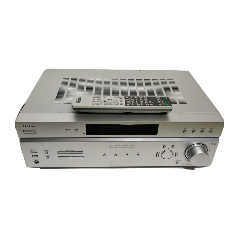
PHOTO:
STR-GX415
SPECIFICATIONS
Amplifier
section
AEP1,
German,
90W+90W
70W+70W
East
European,
(4ohms)
(4ohms)
UK
model
80W+80W
50W+50W
DIN,
IkHz
(80hms)
(80hms)
80W+80W
70W+70W
50W+50W
(80hms)
(80hms)
(80hms)
40Hz-20kHz
THD
0.3%
Harmonic
distortion
Less
than
0.8%
at
rated
output
Frequency
response
PHONO:
RIAA
equalization
curve
+0.5dB
CD
VIDEO
|
10Hz-50kHz
‘3
dB
TAPE
Input
Sensitivity
Impedance
S/N
(weighting
network,
input
level)
PHONO
2.5mV
50kilohms
75d
B(A
net)
75dB*(A
net,
5.0
mV)
CD,
VIDEO,
—
|
250mV
5O0kilohms
82dB
(A
net)
TAPE
1,2
82dB*(A
net
500mV)
*78
THF
Outputs
REC
OUT,
Voltage
250mV
VIDEO
(AUDIO)
OUT
Impedance
10kilohms
HEADPHONES
Accepts
low
and
high
impedance
head
phones
Tone
controls
BASS:
£10dB
at
100Hz
TREBLE:
+10dB
at
10kHz
Loudness
+6dB
(100Hz)
MICROFILM
Tuner
section
Tuning
range
87.5-108MHz
531-1602kHz
Antenna
75ohms,
unbalanced
Sensitivity
at
18.3dBf,
2.2nV
(mono)
41dB
quieting
40d
Bf,
24.5yV
(stereo)
Usable
sensitivity
11.2d
Bf,
1pV
(IHF)
Loop
antenna:
300pV
(at
999kHz)
Signal-to-noise
ratio
70dB
(mono)
/66dB
(stereo)
|
54dB
(at
50mV/m)
Harmonic
distortion
0.3%
(mono),
0.5%
0.5%
(at
50mV/m,
(stereo)
at
1kHz
400
Hz)
60dB
at
400kHz
30dB
at
10kHz
Frequency
response
30Hz—15kHz
“3°
dB
|
—
General
System
Tuner
section:
PLL
quartz-locked
digital
synthesizer
system
Preamplifier
section:
low-noise
NF
type
equalizer
amp
Power
amplifier
section:
pure
complementary
SEPP
Power
requirements
220-230V
AC,
50/60Hz
240V
AC,
50/60Hz
(U.K.
model)
Power
consumption
ara
STR-GX415
STR-GX315
STR-GX215
AEP1,
German
model
|
230W 200W
160W
AEP2,
East
European,
|
165W
130W
110W
UK
model
—Continued
on
next
page—
FM
Stepeo
FM-AM
Receiver
SONY.
FM
tuner
section
AM
tuner
section
£
8
Ei
=z
AC
outlet
(STR-GX415/STR-GX315)
(except
for
U.K.
model
of
STR-GX315)
One
switched
(100W
Max.)
Dimensions
Approx.
430
x
135
x
300mm
(w/h/d)
(17
x
53/8
x
11
7/8
inches)
including
projecting
parts
and
controls
Weight
.
STR-GX415:
Approx.
7.2kg
(15Ib
140z)
STR-GX315:
Approx.
6.2kg
(13lb
1102)
STR-GX215:
Approx.
5.9kg
(13Ib
10z)
Accessories
supplied
FM
wire
antenna
(1)
AM
loop
antenna
(1)
Remote
Commander
RM-U141
(STR-GX415/STR-GX315
only)(1)
Sony
batteries
SUM-3(NS)(2)
Design
and
specifications
are
subject
to
change
without
notice.
Note
This
appliance
conforms
with
EEC
Directive
87/308/EEC
regarding
interference
suppression.
MODEL
IDENTIFICATION
—
Model
Number
Portion
—
Carved
on
back
panel
AEP1,
AEP2,
German,
East
European
model
:
STR-GX215
AEP1,
AEP2,
German,
UK,
East
European
model
:
STR-GX315
AEP1,
AEP2,
German
model
:
STR-GX415
SON
YY:
movetno.ZZZZZZ
FM
STEREO/FM-AM
RECEIVER
VLLLLLLLLLLLLLLLLL
LLL
SERIAL
NO.
ASSEMBLED
IN
MALAYSIA
GX215;
AEP1,
German
model
:
AC
:
220—230V
~50/60Hz
GX215;
AEP2,
East
European
model:
AC
:
220--230V~50/60Hz
GX315;
AEP1,
German
model
:
AC
:
220—230V~50/60Hz
GX315;
AEP2,
East
European
model:
AC
:
220—230V~50/60Hz
GX315;
UK
model
:
AC:
240V~50/60Hz
GX415;
AEP1,
German
model
:
AC
:
220—230V~50/60Hz
GX415;
AEP2
model
:
AC
:
220—230V-~50/60Hz
Note:
There
are
two
type
of
AEP
models
which
are
depend
on
countries.
AEP2:
Model
for
Scandinavian
countries,
Switzerland,
Spain
and
Portugal.
AEP!
:
Model
for
other
European
countries.
TABLE
OF
CONTENTS
Section
Title
Page
45.
“GENERAL
ites
i
initial
eas
3
2.
ELECTRICAL
ADJUSTMENTS
vvvesccescsesssesssesenees
4
3.
DIAGRAMS
3-1.
IC
Pin
Function
¢
1C300
SYSTEM
CONTROL
IC(uPD78043GF-SOX4072)
ss+erer
5
3-2.
Block
Diagram
crrrsrrrssreererecseeeereesessseraueessesceescvsereersens
7
3-3.
Circuit
Boads
Location
POURUUCEESSCCOOCOOSOOSOOSCO
OOOO
OSOSOELCOS
OE
Seer
9
3-4,
Semiconductor
Lead
Layouts
Por
ee ee
eee
CC
Cererrrerrrerrirrrrrrry
10
3-5.
Schematic
Diagram—Main(GX215)
Section—
srrrrrsrrreeees
1]
3-6.
Schematic
Diagram—Main(GX315,GX415)
Section—
15
3-7.
Printed
Wiring
Boards—Main
Section—
crrrrrstrerserererees
19
3-8.
Printed
Wiring
Boards—Display
Section—
rrrrerrsessrreees
25
3-9.
Schematic
Diagram—Display
Section
vrrrrsrrrsttrseereseeees
27
4.
EXPLODED
VIEWS
4-1.
Cabinet
Section
He
eee
wernneewerenrereere
Poe eee
ereereeeeerreraanoensens
29
4-2.
Chassis
Section
Pree
cE
ee
ESE
SE
eeerrrr
errr
ceri
rrrrerrerrrrs)
oom
eeveesereees
30
5.
ELECTRICAL
PARTS
LIST
------ss
eee
sesso
BI
160W
110W
200W
130W
230W
165W
SAFETY-RELATED
COMPONENT
WARNING!!
COMPONENTS
IDENTIFIED
BY
MARK
A
OR
DOTTED
LINE
WITH
MARK
A
ON
THE
SCHEMATIC
DIAGRAMS
AND
IN
THE
PARTS
LIST
ARE
CRITICAL
TO
SAFE
OPERATION.
REPLACE
THESE
COMPONENTS
WITH
SONY
PARTS
WHOSE
PART
NUMBERS
APPEAR
AS
SHOWN
IN
THIS
MANUAL
OR
IN
SUPPLEMENTS
PUB-
LISHED
BY
SONY.
STR-GX415/STR-GX315
Identifying
Parts
and
Controls
STR-GX415/STR-GX315
(1
POWER
switch
[2]
MONITOR
indicator
(page
62.)
(3)
SHIFT
button
(pages
36
and
38.)
4
Remote
sensor
a
STANDBY
indicator
The
STANDBY
indicator
lights
up
when
the
power
cord
is
connected.
(@)
MEMORY
button
(pages
26
and
36.)
(Z}
BAND
button
(pages
30
and
34.)
(B)
TUNING/PRESET
button
(pages
34
and
40.)
[8]
Display
window
+/-
buttons
(pages
34
and
40.)
{1
TUNING
DIRECT
button
(page
30.)
(J
FM
MODE
button
(page
32.)
(J
CHARACTER
button
(page
26.)
(4
DISPLAY
button
(pages
28
and
48.)
(f]
LOUDNESS
button
and
indicator
(page
22.)
VOLUME
control
(page
22.)
(1
BALANCE
control
(page
22.)
[1%
BASS/TREBLE
controls
(page
22.)
(19
Function
selectors
When
the
TAPE
2
MONITOR
is
pressed,
the
indicator
of
the
last
selected
function
also
remains
lit.
But
the
taped
program
selected
with
the
TAPE
2
MONITOR
button
can
be
heard.
20
EON
(TA-NEWS-INFO)
button
(page
50.)
i)
PTY
button
(page
52.)
Numeric
buttons
(pages
30,
36
and
38.)
HEADPHONES
jack
(page
24.)
SPEAKERS
A/B
buttons
(page
24.)
STR-GX215
Identifying
Part:
and
Controls
Front
Panel
STR-GX215
1).
POWER
switch
2)
SHIFT
button
(pages
36
and
38.)
[3]
MONITOR
indicator
(page
62.)
[4]
MEMORY
button
(pages
26
and
36.)
[5]
TUNING
-/+
buttons
(page
34.)
(6)
Display
window
(7)
PRESET
TUNING
+/-
buttons
(page
40.)
[8]
FM
button
(pages
30
and
34.)
{9]
AM
button
(pages
30
and
34.)
TUNING
DIRECT
button
(page
30.)
[1)
FM
MODE
button
(page
32)
{1
LOUDNESS
button
and
indicator
(page
22.)
(3
VOLUME
control
(page
22.)
BALANCE
control
(page
22.)
ff]
BASS/TREBLE
controls
(page
22.)
Function
selectors
When
the
TAPE
2
MONITOR
is
pressed,
the
indicator
of
the
last
selected
function
also
remains
lit.
But
the
taped
program
selected
with
the
TAPE
2
MONITOR
button
can
be
heard.
(1)
Numeric
buttons
(pages
30,
36
and
38.)
{13
HEADPHONES
jack
(page
24.)
SPEAKERS
A/B
buttons
(page
24.)
*‘JEnNueUT
UOTJONAJSUL
WOT
payoeiyxe
St
UOI}eS
SIUT,
TWHANAD
L
NOILOAS
SECTION
2
ELECTRICAL
ADJUSTMENTS
Note:
As
a
FM/AM
tuner
(TU1)
is
difficult
to
repair
if
faulty,
replace
it
with
new
one.
¢
FM
Signal
Level
Display
Adjustment
(GX315,
GX415)
Setting:
FM
RF
signal
generator
Carrier
frequency:
98
MHz
Modulation:
1
kHz
75
kHz
dev.
FM
ANTENNA
75Q
(100%)
terminal
Procedure:
1.
Tune
the
set
to
98
MHz.
2.
Apply
80
dBy,
98
MHz
signal
to
the
FM
antenna
terminal.
3.
Press
the
DISPLAY
button
of
the
unit
to
indicate
the
signal
level.
4.
Adjust
RV1
so
that
signal
level
indication
is
changed
from
[SIG
71
dB
]t0
[SIG
75
«B]
Apply
81
dBu,
98
MHz
signal
to
the
FM
antenna
terminal.
6.
Make
sure
that
the
signal
level
indication
is
|
SIG7SadB
|
If
not,
repeat
step
2
to
6.
wn
(MAIN
BOARD]
(COMPONENT
SIDE)
TU1
FM/AM
TUNER
RVI
(FM
SIGNAL
LEVEL)
ee
Ic}
SECTION
3
DIAGRAMS
3-1.
IC
PIN
FUNCTION
¢1C300
SYSTEM
CONTROL
IC
(uPD78043GF-SOX4072)
FUNCTION
Drives
indicator
tube.
{e)
=
fom
Re)
Drives
indicator
tube.
Drives
indicator
tube.
=
Drives
indicator
tube.
5V
RDS-CLOCK
RDS
CLOCK
input.
G)
NOPoOl;
Rl
alalw
RDS-DATA
RDS
DATA
input.
RESET
output
for
LC7073M.
12
RDS-RESET
Qa
FUNCTION
output
for
tuner.
IF
COUNT
DATA
input.
ESET
System
RESET
input.
=
5
al/O}olg
z
<
o/31ola
is]
rIa}ia
x)
=
ps)
aera
esas
re
ameeraes)
FOWERT
FUNC
SEL
Fixed
“L”.
Oscillation
signal
input
(4.19MHz)
Oscillation
signal
output
(4.19MHz)
FUN
CCW
Operates
the
motor
for
motor
FUNCTION
FUN
CW
Operates
the
motor
for
motor
FUNCTION.
Motor
for
VOL.
“H"
when
DOWN.
VOL+
Motor
for
VOL.
“H"
when
UP.
30
Q
w
»
=
MN
o
4
x<
Nh
<
x<
=
PS
a|/
ua)
>
(eo)
sa
m
Clove
Oo
,
<
ZiZzi2
nd}
-
of=tn
ro)
vu
3
N“
a
=
Cc
aj
/O
TUNER
MUTE
output.
PROTECT
MUTE
output.
FUNCTION
MUTE
output.
PROTECT
detection
input.
RDS
DATA
START
pin.
Remote
commander
input.
Power
ON/OFF
Monitor.
a
nN
a
=
Cc
per}
os
b
a
N
o
a
aol|z
0/6
pel
<
n
=
Cc
4
PROTECT
IN
RDS-START
n|
+
{e)
Vv
Activates
SPEAKER
RELAY.
Activates
POWER
RELAY.
RDS-ID
detection
input.
oD
5V
Activates
standby
LED.
Activates
VOL-LED.
Activates
TAPE
2
relay.
POWER
RY
a
oO
a
D
~)
i
5
an
w
VOL-LED
TAPE2-RELAY
S-DIRECT-RELAY
54
<
Activates
source
direct
relay.
Destination
change-overinput
“H”:EastEuropean
“L”:
AEP,
G,
UK
Model
change-overinput
“H”:GX215
“L”:GX315,
GX415
ss
>
=
wo
<
a
N
Fixed
“L”.
LOUDNESS
CONTROL
output.
Drives
indicator
tube.
LOUDNESS
P15
=
{Nh
Drives
indicator
tube.
Drives
indicator
tube.
Drives
indicator
tube.
Drives
indicator
tube.
Drives
indicator
tube.
Drives
indicator
tube.
fo)
N
Drives
indicator
tube.
Drives
indicator
tube.
Uv
N
70
~
24V
Drives
indicator
tube.
Ls)
Drives
indicator
tube.
Drives
indicator
tube.
N
-
Uv
>
Drives
indicator
tube.
wo
Drives
indicator
tube.
NI
to)
s}]~N
N
NINN
a
rR)
=
a
7
Drives
indicator
tube.
10G
o
Drives
indicator
tube.
«)
Drives
indicator
tube.
©
Drives
indicator
tube.
Q
~
3-2.
BLOCK
DIAGRAM
FM
750
COAXIAL
L—
mw
118
r
L
r
iB
r
E
STR-GX215/GX315/GX415
6X316,6X416
=e
fe
Sate
eee
ee
de
ee
7
1C1
1c2
G:
German
Tu
|
Ic
ROS
DEMODULATOR
ROS
DATA
PROCESS
EE
:
East
European
FM/AM
TUNER
|
one
S7KHZ
RECONSTRUCTION
SERIAL
ROS
|
ROR
DET,
DATA
|
@ ®
@)
‘
oe
BANDPASS
FILTERSS
(6)
PARALLEL
ae
fom
a,
SERIAL
(8)
|
|
CONV,
CONV.
|
3
(8)
2
|
(5)
Or
RDS~
|
sueae
8®5Z248
ROS
YH
-—-—-——-—
!
ae
clock
z
2
7
cLocKED
uae
i
or
DIFFERENTIAL
®
A.B.C.C:D
(16)
|
COMPARATOR
mo
DECODER
(5X6X7X8X9)
e302
N22)
|
FIXED
DIVIDER
DECODER
RDS-
|
START
aa
tt
|
|
|
clock
|
SYSTEM
i
|!
"
4)
osc
REGENERATION
QUALITY
RDS-1D
[ose
|
|
j43Mu
ES
tea
s
&
BIT
(1)
|
I
|
(43)
DIVIDER
SYNC
GENERATOR
a2
|
|
3h
!
|
1C3
C-W)
O-®
|
|
FM
SIGNAL
DETECTOR
||
|
x2
5
|
|
4MHz
Hi
|
ae
|
is
|
|
2
ad
|
|
|
Zz
|
a
FM
IF
ANP
3
|
LIMITER
|
seis
1¢401
|
eae
|
am)
!
|
PHONO
I
1
t
E
i
O-
©)
couatizer
[7O
ha
Se
ee
ee
se
Se
|
1
1
!
f
10402
! {
PHONO
1
1
rR
!@
t
(4)
PoNRCizeR
(2)
FUNCTION
SW
y708
ete
! |
RY4041
ou
an
a4oz
7f--.
10306 10403
av701
be
=
~
ae
8
a
!
T
:
t
1
-
ON
r
|
@+—-—_
G6)
!
13
1
TONE
1
4fri2.3cB]
2
1
Q701-707.712,713
Na
1
C)
'
ON
\ i
f
fT
es
VIDEO
Leo
!
aa
1
[CONTRO
a
\
‘AMP
454;
5!
L
cH
;
|
>
L
mt
iGo
poy
avo
De
Ty
avioz
|
ras
*"|_POWER
AMP
Vv
1
Wy
*|
1
'
=
a
Oo
‘
REcoUT
|
I
yea
AT:
(REBLE
J
»
I
|
OFF
b
LriGOo
'
re
i
1
-
i
t
1
'
OFF
i
H
AOA
'
1
BALANCE]
°)
i 1
q
1-4
402
'
arc
:
1 1
i
i
1701-3
701-2
R
.
6!
'
1
1
16306
a
T
1C403
a
oe
in
oe
toi:
(172)
Zs!
Bs:
1
(172)
'
an
'
!
1
1
!
L_rei@G@s
1
ers
z
TONE
n__
brig
hr
12.305]8
'
|}
Q751-757,762,763
i
'e
oi
oa
an
=>
!
;
|
=
ike
La
ST
eyo
te
:
AUD
Oe
OUT
i
\
NI
1
H
1
ot
0714,764,71
\
8
Lr!@9
1
i
»
1 1 ! '
ee
sot
a
oe
et
OVER
DC
OFFSET
’
.
L'16
1
w
a4o8
1 i
tt
LOAD
DET DET
!
H
O
aio
ia
|
i
2
RELAY
!
Pog
Lon
aa
teeta
©
d
z
DRIVE
LOUDNESS
'
1
ot
R
on
Be
1
=
>
M.VOL+
tO
TEA!
6xX316,6x416
|
{
1
S
s
I
om
mt!
Gr
5
Fe
OFF
IN
!
H
g
S78
ore
1
!
ws
Lo
Re
16
i
z
$701-2
1 1
! i
$701
! 1
D705 0718
rt
1
©
PROTECTOR
RecouT
| H
|
SPEAKERCRY
RELAY
Lr!
©
-
[>e
DRIVE
laneeal
0749
LCH,RCH
+8
POWER
AMP
-B
T90l
0
eee
=
1,095:
cnc
i.
fea
eee
See
sats
ad
20
2
p95
sauce
[-
71
(
16401~403,
306,
TU1
)
+12V
TRANSFORMER
énieun
I]
6X216:0953
D955
nee
'
=~
=
Ta
Hd
(1¢401~403,306)
-1av—4
2
ies
t
pgge
|lienan5
scone
1
A
REG
09520953
H
11
ON
N35
D306
(16300)
-24v
v
OX316:AEP,
eau.
|
9302_
(MONITOR)
REG
‘here
|
x“
<[e
[r
jo
Cn
Cea
ara
LED
(i)
3
F
:
ele
x1
DRIVE
(FL300)
F
<—
1
iz
c--ca4
8214/8
Q3o1
X28)
976,977
|
|
ia
oe
lee
x2
Ma
|
FL300
LED
oz
ae
[ease
i)
tek
es
ef)
FLUORESCENT
a
DRIVE
N7
|
|
oer
Tt
6X316,6X415
EMOTE
902
INDICATOR
1€300
0305
L
Jt
power
|
ie
'
SYSTEM
CONTROL
TAPE2-RELAY
a303,304,
30LCUDNESS)
p=
—
—
—
—ITRANSFORMER
|
i
LGuaKESS
a953,0962
||
n966-969
| 1
7
LOUDNESS
SSS
>
Tu
eo
re
ae
ee
!
'
Palicioe
16300,
301,302
REG
' H
aaa
VoL+
|
954-957
|!
p970.971
|
|
$315-330
_$301-313
|
iol:
<
sy
4
Motor
[7
M.VOL-
|
Ste
a
le
tee---s
FUNCTION]
[FUNCTION
SeaneEy
DRIVE
|
'
o
|
SWITCH
SWITCH
|
Q300
%
D304
|
te
4
|
LEO
|
4X
(STANDBY)
|
6X316,6X416
—
oxaie.
I
orive
|
©
a
a
ee
=
!
H
RESET
i301
|
SOOT.
per
PROTECT
IN
-=
--=
|
Rewore
|
|
Say
a
/
0306
avo
|
CONTROL
BOWER-RY.
60
POWER-RY
FOWER
RELAY
|
i
RECEIVER]
|
ry
siitcu
aaWe
|
8137
|
SE
Se)
|
ie
RESET
|
|
oN/STANDBY
|
|
foe
OSS
HO
AE
J
L
eae
as
J
6X316,6X416
G6X315,6X415
3-3.
CIRCUIT
BOARDS
LOCATION
AC
SW
board
(GX215
model)
POWER
board
TRANS
(SEC)
board
STAND
BY
board
(EXCEPT
GX215
model)
MAIN
board
SW
(3)
board
JOINT
(1)
board
SW
(1)
board
SW
(2)
board
JOINT
(2)
board
DISPLAY
board
VOL
board
TONE
board
3-4.
SEMICONDUCTOR
LEAD
LAYOUTS
BA6208
uPC4570HA-1
2SA979-FG
.
BCECB
2SA988-PAFAEA
|
623456789
G1U58XB
me
123
1
Vout
oe
/fr
Ec
B
M5218AL
2SA1175-HFE
2SC2785-HFE
2SC3623A-LK
DTA124ES
DTC114TS
12345678
LETTER
SIDE
RBA-402
i
f
:
Ed,
(TOP
VIEW)
2SB734-34
2SB1375-LC
2SB1560-OPY
2SB1587-OPY
2SD2390-OPY
2SD2438-OPY
|
u
H
2SD809-K
LETTER
SIDE
28D2012
f
M
\
E
Ay
BCE
2SA1221-K
2SC2958
2SK246-GR3
~e
o-”
DTC124ES
UZ-12BSB
UZ-13BSB
CATHODE
ANODE
HZS6C3L
UZL-24L
UZ-4.3BSB
UZ-6.2BSC
cathode
anode
RBV-602-01
SEL3210S-CD
SEL3810A-CD
long
short
anobe
cathode
3-5.
118
SCHEMATIC
DIAGRAM
—MAIN
(GX215)
Section—
1
2
3
4 5
6
7
8
9
10
11
12
1¢
v
a
-
[
MA
I
N
BOARD
]
9701-707.
712,
713
s
zg
[B+]
F006
9g
42.5
L-CH
POWER
AMP
Shar
ote
ee
-
!
is
.
8798
2
Bibs
0.6
|
28;8%o
c726
97K
ieee
EE
1.
=
8
rt
ae
yy)
1
R701
if
gro)
Le
79
C705
3p
{
JOINT
(1)
_BOARD
1]
[
JOINT
@)
BOARD
}
FE
=>
Ke
CNPII3
D
ry
a
S
Ll
{10
|
=12V
702:
2
—
=)
wy
&
:
=>
.
foo
co
eee
|
Pf
no
f}
eae
|
a
CNP103
ol
=
{
{~
N—
‘
——
(See
Page
28)
ci
{
2
|
L.IN
a
J
T
[
oSCsSY
Np
enrsoe
CNu402
36.9,
1
()-
0.6
C791
Seeoieeeeeee
ee!
me
EQ
AMP
‘x
=
g
of
eh
€
Otte
E
3
g
1
Cael
§82
cia
£408
"|
ays
p60
Hie
1
ay
yen,
05
DO
7
uy
rte
ae
SP
>a
4
cape
£406
[9.8
per
Tis
except
6
q
00
1000
Bee
7
Q751~757,
762,
783
Fle
-
nN
yy]
R-CH
POWER
ANP
P
at
8
—
&
3
C.
7.
I
oreaai
0
2
:
al
tp
tots
7
z
a
J
3,
J403
|
ui
Ox
[PHONG]
ie
10306
(1/2)
M5218AL
H
+
12.6
Roz
ik
POOF
a
7
0.0048
PT
[1C402]
CH
|
FUNCTION
AER.
e
ra
tate]
Fe
Bh
>ah
=
aa
SWITCH
R305
820
ry
‘
len
°
+H
BUFFER
AMP
means:
®
iis
Bia
10306
(2/2)
MS218AL
3a
oh
&
Hea
oe
na
Ht
TO
BISPLAY
BOARO
CNJI01
(See
page
27)
R407
4.
rl
2
3
1
1N41
48M
C981
0.0225
X
=H
11
Q751-757.
762,
763
12
41.8
0703
2802785
R-CH
POWER
AMP
14
R713
670641.7
Ff
22
68)
,
05
501
()
2D
1d
i
C705
3p
PROTECTOR
Y
BOARS
101
ge
27)
Qs58
PRESET
®ET
cape
ey
i
AEE
Sma
2
Pel
16 17
18
19
Q714
715
OVER LOAD
BET
L7o1
[R737
10
|
ul
L
C711
O18
R787
10
Lp!
L751
716
717,
€C
OFFSET
W
77
22
(
%&
Pi
Ht
F828
t
1
ST
NT
Peg
eg
ee
Re
a
eget
al
Uy
20
5
1
S
1
R796
10
Air
R74
10
:
It
21
22
23
N
[
SW
(1)
BOARD
}
eee
[6
0
0
OO
_
a
=z
N
Py
oro
>
o>
nn
es
*o
iets
ie
OF
B76
rH
(CHASSIS)
pibwercewaesroteloude
eect
LOQQVQQO0
[AC
SW
BOARD
}
ae
mt
T
Ee
Bt
/
[INPEBANCE
USE
i}
8-160
d)
te
{
SW
(2)
BOARD
]
[
HP
(1)
BOA
[
HP
(2)
BOA
a
*NOT
REPLACEABLE:
BUILT
IN
TRANSFORMER
1
oof
Zoov
1
oot
doov
>
(CHASSIS)
(
SW
(1)
BOARD
}
[
SW
(3)
BOARD
}
i
=a
I
A701
1
Ne"
Cet
Pe
a:
—
Lol
i
j
iio
++
|
foie
Sd
J
oh
ae
el
ae
See
:
—
teh
)
|
|
|
B
A
;
@!C
Block
Diagram
Se
ra
_|
cee
|
1C402
LC7822
ia
['Sw(2)BOARD}[om]
|
[0
er
ye]
ae
Efe
ey
a)
PERE
CHP
(1)
BOARD
J)
| |
ag
inp
3
—-.-
xx
Oo}
A+
R}
Ll,
B+
|
|
TNPEOANCE
|
a-lga
!
:
!
{
HP
(2)
BOARD
}
ee
o
(CHASSIS)
|
S
7
ee:
72.
1.2K
R791
x
*NOT
REPLACEABLE:
BUILT
IN
TRANSFORMER
a
9°
a
=
Zz
fe}
oO
@
All
capacitors
are
in
uF
unless
otherwise
noted.
pF:
uwuF
:
internal
component.
°
Eg
:
nonflammable
resistor.
|
Note:
\
SOWV
or
less
are
not
indicated
except
for
electrolytics
L
and
tantalums.
es
eee
oF
|i
ena
A
@
All
resistors
are
in
2
and
/,W
or
less
unless
otherwise
Al
it
a
specified.
{
cNug01
<
A
Ad
|
ry
:
B+
Line
e
:
B—
Line
Note:
The
components
identified
by
mark
A
or
dotted
are
critical
for
safety.
Part
number
specified.
line
with
mark
Replace
only
wit
®@
Voltage
is
dc
with
respect
to
ground
under
no-signal
(detuned)
conditions.
©
Voltages
are
taken
with
a
VOM
(input
Impedance
10M
2).
Voltage
variations
may
be
noted
due
to
normal
produc-
tion
tolerances.
@
Signal
path.
>
:FM
e@
Abbreviations
G
:
German
EE
:
East
European
e@
IC
Block
Diagrams
1C402
LC7822
mes
@)—®)
{\
y
i
O—®
Y
(&)—8)
@)—®)
®
Hecal
oes
(~)
(8)
CONTROL
SHIFT
REGISTER
Note:
e@
All
capacitors
are
in
wF
unless
otherwise
noted.
pF:
uwyF
50OWV
or
less
are
not
indicated
except
for
electrolytics
and
tantalums.
e
All
resistors
are
in
2
and
'/,W
or
less
unless
otherwise
specified.
e
4
_:
internal
component.
)
End
:
nonflammable
resistor.
Note:
The
components
identified
by
mark
A
or
dotted
line
with
mark
are
critical
for
safety.
Replace
only
with
part
number
specified.
:
B+
Line
:
B—
Line
(C_]J:
adjustment
for
repair.
Voltage
and
waveforms
are
dc
with
respect
to
ground
under
no-signal
(detuned)
conditions.
no
mark
:
GX415
or
common
(
):
G@X315
e@
Voltages
are
taken
with
a
VOM
(Input
Impedance
10M).
Voltage
variations
may
be
noted
due
to
normal
produc-
tion
tolerances.
@
Waveforms
are
taken
with
a
oscilloscope.
Voltage
variations
may
be
noted
due
to
normal
produc-
tion
tolerances.
e@
Circled
numbers
refer
to
waveforms.
e@
Signal
path.
>
:FM
e
Abbreviations
G
:
German
EE
:
East
European
IC1
SAA6579T
QUAL
RADA
o
n
©
bal
On
ao
ao
>
i
Vref
¥3G033G
TORWAS
3SVHdIG
MUX
VopA
Vssa
BOVLIOA
3IN3Y3434
INAS
GNY
NOLLVY3N3934
49019
Y3aGIALG
G3XxI4
GQNY
STEVIYVA
do0T
SViSO3
YOLYYVdWOS
6323073
SCOUT
()
HAGIATG
(dAGYO4
48)
yalqd
YOLVYSN39.
Ld
ALIAS
GNY
yOLYTII3SO
SSVdGNVE
ONISVIWV
ZHALS
NOTLINYLSNOISYH
-TLNV
HILIMS
¥O193973S
iNdinO
@NY
31907
LS3L
CORR.
cL.Ed.
IC3
LA1235
MUTING
CIRCUIT
NULL
METER
SHORTING
5
FM
IF
AMP
QUADRATURE
LIMITER
om
|
bel
RACL
157
asco
OSC!
Veo
Vssa
TEST
TSTLA
RECEIVE
3-6.
SCHEMATIC
DIAGRAM
—MAIN
(GX315,
Gx
[JOINT
(1)
BOARD]
[
JOINT
aoe
L
TO
VOL
BOAR®
CNP103
(See
page
28)
CNP404
EQ
AMP
1
§
PUSOR
15.1
Treo
ae
408
ag
[Me]
ose]
bi
AS
PERT
Tt
[p=
408
Gage
0.5
1
!
EXCEPT
G4
{90}
BP
oS
BE
Ray
220P
cameel
Cat
eb
hake
ale
: ;
lites
or
ke ZT
sty
TY
a
—Te]
S|
=:
é
Bs
I
J403
|
oO
Os
|
4
(PHONO)
'
~
U_§_a
@+
pos
oe
d
oO
;
a
if
i
R471
180
2.8.8.6
ii
<r
ia
(9)
@
(9)
R486
1k
@)
118
—MAIN
(GX315,
GX415)
Section—
4
5
6
(1)
BOARD]
[
JOINT
(2)
BOARD
]
CNP404
EQ
AMP
401
ETEK
13.1
R415
820
MSS
®
Waveforms
@
2:
4.33
MHz
14.5mV
10
11
12
0:
4.33
MHz
25mvV
ee
4.0MHz
4.4V
i
[
T
17
18
1s
R471
180
Q402,
752
MUTE
POWER-RY
‘SPEAKER-RY
e
G
8
#
ROS-1D
818)
Fale
2/2]/2
TUNER-MUTE
FUNCTION-MUTE
ROS-START
=
[ox
Pe]
DATA
a0]
CNJ102
=24V
PROTECTOR
STEREO
o
I
|
TO
QISPLAY
BOARD
CNJ101
AM
OC
(See
page
27)
T™1
*
[ANTENNA]
FM
75.9
q
COAXIAL
©
Ras
DEMOBULATOR
a
——+-
[
MAIN
BOARD
]
{i
J
een
al
4
:
Q701-707,
712
713
ae
Gin
Ke
cys
OVER LOAD
BET
L=CH
POWER
AMP
£
&
aN
701
She
T
a
fe
R738.
10
47.1
0.6
£728.
+
Glen)
[47]
EXCEPT
6
9715
R732
2sc27e5
ik
=
-54.7
7:
es
(46:8)
F233
+
omy,
res
R701
c701
16V
i
t
«4.78
SOV
Wr——)
F
=>
AW
R718
22
c7oz
L
R703
R702
S205
7
Ye
FOU
LS3.
[B+]
SS
a
EE
|
T
R756
53.2
|
560
(47.3)
oe
53
R754
7
4
wee
ke
Oe
Hi
(47.
2a
eee
54.2
iat.
R767
48:2)
47
R757
Pr
10
ree
l
ee
Oe
ty
a
Wy
ww
9752
a755
0
0.69
204888
ies
9756
238300
2982012
776,
4
.
R776
=
c755-10
0,23
I
751
=
0.6
7s)
=
ws
73
Feze
[EXCEPT
G
BB
F
ATES
c759
BW
te
BOV
5
9757
-
Be
8
me
54.7188
0764
Q716
717
‘)
g
i
(47.8)
rage
48.)
|
88
OVER
LOAD
BET
QC
OFFSET
AW
—+—4
4—
‘Mp
Ll
R745
>
33
+
0751-757,
762.
763
R-CH
POWER
AMP
9951
RBVa02
1
ES
0.
088"
hoov
+
956
6
NAT
48H
c9S2
+
0.068%
toov
R9s9
10B%
w2Fiisa
+
=
cage
R960
>,
£96
4.740
50V
10306
(172)
MS218AL
we
=
.
12
95
<i
R305
820
peAV
ORES,
38
T
z
S
1S
BUFFER
AMP
VE
SS
7
955
+5V
REG
ES)
3
4
ee
|
ecient
5
|
ie
0958
BAIF4M
R3SS
820
s
xl
>
979
ei
z¥
ape
o
2
C2PlEXcePT
G
s|-
Seen
ay
(20°
c
s\3
ry)
=
3/8
2
4
i)
3
ee
a
(ear
ae
.
2
a
o3
8
a)
ala
az
0958
Q954-957
977
Fi
0
PRESET
ET
STOP
ET
obits!
ty
Te
Raps
9406
2
BNIF&N.
R427
=
R430
4
__|
x
cs
4
zg
—+—
PER
n) a)
a}
ol
wo
5]
A)
2]
a
a
0,
BaLi3[
oe
esis
&lg
Ea
}_}
Ses
S/s
C9)
ay
ss
»
|
$
@
felelalsl
alg
EAC,
222705
t
a
rars
Par
Tee
0437
eo.
BATAAZ
080
aarvaceman!
0408
——p
ast
+s
12.6°|
RELAY
DRIVE
o| af
—|
of
of
Sal]
oo
m9
A
ata]
3
0406
INVERTER
Life
|
he
a
R7
100K
14
NJM45589_
4.4V
Ic2
©
4.0
MHz
@
«
4.0MHz
5.0V
+
+
nb
V
|
|
|
|
i
4
b
peg
ae
ane
mer
So
he
16
17 18 19
20
21
22
23
24 25
26 27
28
{
SW
(1)
BOARD
]
[
SW
(3)
BOARD
]
Se
ea
a
ee
ee
eet
Se
eee
a
—-=
ee
ee
ee
es
3
Q714
715
|
L198
OVER LOAD
BET
3
8
va
L704
ong
i.
vero
Fel
©)
t
719
:
L
INVERTER
i
fa
eee
Cf
to
Fry
R790
my
ING
"TOK
I
WAL
Oo
27,
1
(“)
252185
5
J
US
0
R744
p
0-7
"tox
[971
r
t
54.7
SY)
Buea
?
8-a)
EC)
705
z
=}
y
Nei
aaH
1
ys
718
SPEAKERS]
A
RELAY
Pop
ete
Ss
RIVE
|
.
=
ON
I
-
mm
baie
we
[
SW
(2)
BOARD
J
,
D1
ore
=
fag
|
|
o}
At
!
eee
Se
R799
i
|
LH,
i
a
|
of}
A-
[SPEAKERS
[
HP
(1)
BOARD
]
CNB
04
ai
|
ESET
fs
pe
R788.10
iy
o|
At
a
Es
1
o|]
Bt
|
jd
@)
;
OT
|
I
INPEDANCE
28
a764
0716
717
|
8-160
7,
|
58
OVER
LOAD
DET
BC
OFFSET
|
19)
|
8B
|
|
|
|
i}
Ls
+
AN
pavile
(CHASSIS)
0,088
toov
=
|
EY
Ba
iss
=
‘aa
952
J701
2S
Toe
!
HEADPHONES
3
3
Bs
Ie
cussis
&
TRANSFORMER
BOARD
]
2
J
(Ba)
7
5S
_ ~ ~
=
ES
a
ee?
!
it
ETE
[
|
ste
S.
™
ca77
Ve
PROCESS
s?
a:
=
as
aS
SS
33
C984
1000
25
Qg59
Q960
LE®
PRIVE
RELAY
SRIVE
{
POWER
BOARD
]
[|
RY9O1
A
*NOT
REPLACEABLE:
BUILT
IN
TRANSFORMER
F902
11,
6AL/250V.
2
a
aa
t-
AEP,
G,
EE
cNy902
A
AC_OUTLET)
OO
(CHASSIS)
FM
SIGNAL
I
I
geTecToR
|
I
3-7.
PRINTED
WIRING
BOARDS
—MAIN
Section—
®
See
page
9
for
Circuit
Boards
Location.
®@See
page
10
for
Semiconductor
Lead
Layouts.
[Ti
2
|
3
|
4
5
|
6
|
7
|
8
|
9
io
|
oo
12
|
3
|
14
15
16
™1
$603
J402
J601
foetal
A
em
ia
[$3]
Ree
oun)
iN
Rupr
ous
tAUBTO“IRD
Aaa
TANF?
ee
USE
a
:
AM
Paar
lpg
R
L
R
L
R
L
R
L
R
L
R
i
R
L
R
L
B©@
A@_
BO
AO
BO
AO
_
BO
A®@
©
{ |
O+©
@+©
@+o©®
F+o©
@+,©
FG+O
EG+O©
O+©@
ee
ee
ee
ee
ee
ee
[MAIN
BOARD
]
|”
ae
eles
cies
Wipes
of
ae
—
i
B
C
(CHASSIS)
D
E
F
G
1-647-633-((14)]
{
JOINT
(2)
BOARD)
[
u¢
H
|—-<1
1-648-998-[(14)]
|
4~_
J
i
1-647-611-
2
A
(CHASSIS)
3
=—
L
|
Tepes
BOARD
(See
page
25)
[
J
|
15
6
|
wf
iw
|
9
|
2
21
rn
GXS1B:AEP.G.EE
OX415
¢
Semiconductor
Location
[
TRANSFORMER
BOARD
]
a.
<2,5>
H-5
C-7
J-5
1-2
C-9 c-9
[
POWER
BOARD
}
F-6
C-7
a
G-6
F-6
1-7
F-6
ae
aI
J-9
F-7
a
G-7
G-6
|
E-6
H-7
|
F-6
H-9
|
D-8
G-7
iGHassisit
H
D
=
16
|
~
9
[a4
F-8
G-9
yy
ee
ea
ep
eee
4-647-631-
11)
|-4
H-7
iy
|
*NOT
REPLACEABLE
G-5
H-7
Deena
4]
BUILT
IN
TRANSFORMER
G
=
7
G
x
6
G-5
G-6
H-6
H-6
1-7
H-5
CNJ904
J
-
8
E
—
6
D964
1-8
Q752
E-6
D965
1-7
Q753
E-6
[sw(1)
BOARD]
[SW(2)
BOARD]
pe66
|
J-7
Q754
|
F-6
a
D967
|
:
7
Q755
D
:
7
[Sw
(3)
BOARD)
Egos
pes
|
1-7
||
Q756
|
E-9
;
ie
SS
D969
1-7
Q757
E-7
jEAC
SW
BOARD
}
D970
|
J-7
Q762
|
F-9
o
:
D971
J-7
Q763
D-9
an
pe76
|
F-7
||
a7ea
|
E-8
D977
F-7
Q951
1-3
Q952
H-5
IC1
F-3
Q953
J-8
IC2
G-3
Q954
J-8
IC3
E-3
Q955
b=Z
1-667-633-(4f
te
e7-636-
NS)
PY
ee
ee
LL
IC4
E-2
Q956
1-7
Ic306
|
E-5
||
Qo57
|
H-7
Ht
C-3
H-7
C-5
H-5
HEAD
PHONES
ee
Note:
@
o——:
parts
extracted
from
the
component
side.
[HP
(2)
BOARD]
e
:
parts
extracted
from
the
conductor
side.
aes
a
@
Abbreviations
G
:
German
EE
:
East
European
vous
se
1-648-997-
|
1-647-637-J1(11)
1-647-636-
t
[HP
(1)
BOARD]
TO
VOL
BOARD
CNP103
(See
page
25)
—21-—
—99—
3-8.
PRINTED
WIRING
BOARDS-—DISPLAY
Section—
®
See
page
9
for
Circuit
Boards
Location.
®See
page
10
for
Se
@
IC
Block
Diagrams
ma
nz
2
|
3
L
4
)
|
6
the
i
ie
8
|
.
1C302
BA6208
[DISPLAY
BOARD]
0
TO
MAIN
BOARD
(See
page
19)
A
CECT
cnsto2
D
dedechedeohuchedobchidibodedmobbedbecbed
bed
pedeohedeed
deed
,
B
C
@®
Waveforms
D
(C300 (C300
@5)
0
4.19MHz
Q
4.19MHz
3.9V
5.3V
—
T
t
E
{
F
[VOL
BOARD]
{
TONE
BOARD
}
Location
G
H
Note:
@
o——:
parts
extracted
from
the
component
side.
|
@
—:
parts
extracted
from
the
conductor
side.
@
Abbreviations
G
:
German
B-10
EE
:
East
European
C-2
|
14
|
C-1
7-607-632-
[11]
C-2
Cr4
-
A-10
C-2
|
=
2
J
18
a7
-629-\(11)
1-3
ica
(BD
“encugs
COA?
(See
page
21)
NC
tor
Location
3-8.
PRINTED
WIRING
BOARDS-—DISPLAY
Section—
@See
page
9
for
Circuit
Boards
Location.
@See
page
10
for
Semiconductor
Lead
Layouts.
Oe
aa
ee
ee
é.
|.
fo.
|.
o—
|
40—
hth
(DISPLAY
FM
_
MODE}
E
[VOL
BOARD]
[
TONE
BOARD
}
SSeS
as
Si
i}
\
er
|
ene
ee
Gegeaee
wee
oF
he
UH
A
FA
|
|
|
1-647-632-
(11)
118
eer
(11)
T
BOARD
(©)
“enscoe
(See
page
21)
=20> —26—
GX315,GX415
eS
Se
{
STANDBY
BOARD
}
POWER
12
3
|
14
15
A
TO
MAIN
BOARD
a
CNJ102
(peerage)
GX416]
J106
1
|
Z
|
al
4-647-628-
[—
{(14)]
3-9.
SCHEMATIC
DIAGRAM
—DISPLAY
Section—
1
2 3
4
5 6
7
10
11
A
B
a
[DISPLAY
BOARD]
.
|
FL300
1
FLUORESCENT
\
|
INDICATOR
TUBE
D
{
G6X315,
GX415
os
cNst02
0303,
304
306
7
=
MOTOR
BRIVER
LOUONESS
SWITCHING
[oe
E
re
=
ato
nveue
4}
2
-eEC
[3
|
ou
=
ae
[2].
|
;
N
K
”
0
Lif
xe
3
als}
|S
F
2
CNUIOT
||
MONITER
LEB
SWITCHING
|
SYSTEM
CONTROL
i
REMOTE
CONTROL
RECEIVER
R533_100
ra
;
=
R335
100
&
H
@
TO
MAIN
BOAR®.
CNJ102
(See
page
12,17)
l
J
K
L
M
18
TECT-IN
ATA
3
|
START
Nininirin[s
= =
Note:
e
All
capacitors
are
in
wF
unless
otherwise
noted.
pF:
uwuF
SOWV
or
less
are
not
indicated
except
for
electrolytics
and
tantalums.
al
ol
itil
|
li
a8
-
—yy_F836
100
8
L__p
rn.
a30S
POWER
RELAY
SWITCHING
12 13
1
4
(VOL
BOARD]
15
16
17
{
TONE
BOARD
}
C508
3.3
50V
—
C558
3.3
SOV
UP®78043GF
-SOX4072
45V
A/B VOR
‘S315
S316
1.5K
1300
10sH
R347
10K
85
Be
J
R511
100%
ORIOR
ses
71%
1
1
Cer
ri
:
“feet
S137
cnet
i
po
L)
Ee
GX315,
GX415
S317
100
igd
gerd
“gg
4
30,
9
are
SWITCHING
|
:
H
t
Hi
Hi
‘
H
‘
i
H
H
H
i
H
H
!
H
H
{
a
iE:
\
[erRecTy
R303
Were
20
aaa
gt
o3
G
$318
bane]
$319
$320
3321
fi
i]
p16]
psi
GERORY
psig
GGHIET
psy
O
wz
@
8
120
we
MS
We
10
bei
a
18
CNPIO9
GX315,
GX415
GX315,
GX415
9
GX315,
GX415
|
ae
ERT
S305
$301
|
5302
fersecav])
(runtnozpre
$322
|
|
al
Ul
|
Note:
The
components
identified
by
mark
A
or
dotted
line
with
mark
A
are
critical
for
safety.
Replace
only
with
part
number
specified.
e@
All
resistors
are
in
Q
and
'/,W
or
less
unless
otherwise
e
:
B+
Line
specified.
:
B—
Line
e
4:
internal
component.
e@
Voltage
and
waveforms
are
dc
with
respect
to
ground
e
under
no-signal
(detuned)
conditions.
e
Sign
—27-—
no
mark:
FM
[=p
al
path.
>
FM
@
Voltages
are
taken
with
a
VOM
(Input
Impedance
10M
®).
Voltage
variations
may
be
noted
due
to
normal
produc-
tion
tolerances.
@
Waveforms
are
taken
with
a
oscilloscope.
Voltage
variations
may
be
noted
due
to
normal
produc-
tion
tolerances.
Circled
numbers
refer
to
waveforms.
e
Abbreviations
G
:
German
EE
:
East
European
19
20
TO
JOINT
BOAR®
CNP404
(See page
11,
16)
SECTION
4
EXPLODED
VIEWS
4-2.
CHASSIS
SECTION
NOTE:
@
-xx,-x
mean
standardized
parts,
so
@
Items
marked
“
*
”
are
not
stocked
The
components
identified
by
mark
A\
or
they
may
have
some
differences
from
since
they
are
seldom
required
for
dotted
line
with
mark
A\
are
critical
for
safety.
the
original
one.
routine
service.
Some
delay
should
be
Replace
only
with
part
number
specified.
@
Color
Indication
of
Appearance
Parts
anticipated
when
ordering
these
tems,
|
ty
Example:
@
The
mechanical
parts
with
no
reference
\UK
model
i
KNOB,
BALANCE
(WHITE)...(RED)
number
in
the
exploded
views
are
not
Note:
:
'
0,
H
t
t
supplied.
There
are
two
type
of
AEP
models
which
are
aa
;
Sy
i
Eee
|
Parts
color
Cabinet’s
color
@
Hardware
(#mark)
list
and
accessories
depend
on
countries.
oe
Sr
all
OO
CNJ907!
and
packing
materials
are
given
in
the
AEP2:
Model
for
Scandinavian
countries,
s
r
GIS)
ay
eeyreprTy
UK
1
last
of
this
parts
list.
Switzerland,
Spain
and
Portugal.
:
i
model:
@
Abbreviations
AEP!
:
Model
for
other
European
countries.
4-1.
CABINET
SECTION
G:German
_
EE:
East
European
7!
poco
c
oct
rn
GX315:
AEP,
G,
EE/
at
eee
VA
GX415
model
Ne
te
a
ete
ee
R
r
i
!
\
if
!
EXCEPT
LE
6x2
16
model
pean
7,
SS!
|
GX415
model
The
components
identified
by
mark
A\
or
dotted
line
with
mark
A\
are
critical
for
safety.
Replace
only
with
part
number
Ref.No.
Part
No.
Description
Remark
Ref.No.
Part
No.
Description
Remark
51
4-917-460-01
KNOB,
POWER
(GX215)
*
65
3-703-244-00
BUSHING
(2104),
CORD
%*52
1-647-637-11
HP
(2)
BOARD
66
4-947-010-01
SCREW,
FEEDER
FIXED
*53
1-647-636-11
HP_(1)
BOARD
*
67
4-965-078-11
PANEL,
BACK
(GX315:AEP2,
EE)
04
4-951-801-01
BUTTON
(S)
*
67
4-965-078-21
PANEL,
BACK
(GX315:G)
*
55
1-652-233-11
AC SW
BOARD
(GX215)
*
67
4-965-078-31
PANEL,
BACK
(GX315:UK)
*
56
1-647-633-11
SW
(1)
BOARD
*
67
4-965-078-41
PANEL,
BACK
(GX215:AEP1/GX315:AEP1)
*57
1-647-634-11
SW
(2)
BOARD
*67
4-965-078-51
PANEL,
BACK
(GX215:AEP2,
EE)
a
mae
*58
1-647-635-11
SW
(3)
BOARD
*
67
4-965-078-61
PANEL,
BACK
(GX215:G)
Ref.No.
Part
No.
Description
Remark
Ref.No.
Part
No.
Description
Remark
*
59
1-647-638-11
POWER
BOARD
*
67
4-965-080-01
PANEL,
BACK
ree
————_
a
*
60
1-647-631-11
TRANSFORMER
BOARD
*
67
4-965-080-11
PANEL,
BACK
(GX415:AEP2
1
4-957-383-01
KNOB
(F14)
8
1-696-456-11
WIRE
(FLAT
TYPE)
(31
CORE)
2
4-949-659-01
KNOB
ae
erie
9
3-704-366-01
SCREW
(CASE) (M3X8)
*61
4-924-098-31
HOLDER,
PC_
BOARD
*
67
4-965-080-21
PANEL,
BACK
(GX415:G)
2
4-949-659-11
KNOB
(VOL-NEW)
(GX215
*10
4-951-795-01
CASE
*
62
1-648-997-11
JOINT
{3}
BOARD
68
X-4941-292-1
FOOT
ASSY
(F58175S)
3
4-958-991-01
PLATE
(VOL),
LIGHT
GUIDE
(GX315)
*11
A-4369-228-A
VOL
BOARD,
COMPLETE
(ax3
15)
*
63
1-648-998-11
JOINT
(2)
BOARD
69
3-318-688-31
FOOT
(F58175S)
4
3-350-426-01
SPRING,
RING
(GX215/GX315)
*11
A-4369-558-A
VOL
BOARD,
COMPLETE
(GX215
*
64
A-4369-227-A
MAIN
BOARD,
COMPLETE
Bares
70
4-923-836-21
CUSHION
*
64
A-4369-229-A
MAIN
BOARD,
COMPLETE
(GX315:G
A\CNJ901
1-696-570-21
CORD,
POWER
(UK)
5
X-4944-688-1
PANEL
ASSY,
FRONT
ere
¥*11
A-4369-562-A
VOL
BOARD,
COMPLETE
(GX415)
5
X-4944-689-1
PANEL
ASSY,
FRONT
(GX215
*12
1-647-632-11
TONE
BOARD
*
64
A-4369-230-A
MAIN
BOARD,
COMPLETE
(GX215:AEP)
A\CNJ901
1-575-651-11
CORD,
POWER
(EXCEPT
UK)
6
1-654-001-11
STANDBY
BOARD
(EXCEPT
GX215)
13
3-575-039-00
NUT,
CONTROL
*
64
A-4369-554-A
MAIN
BOARD,
COMPLETE
eee
A\CNJ902
1-526-794-11
OUTLET,
AC
(GX315:
AEP,
G,
EE/GX415)
*7
A-4369-553-A
DISPLAY
BOARD,
COMPLETE
eles
14
4-942-568-01
EMBLEM
(NO.5),
SONY
(GX415)
*
64
A-4369-560-A
MAIN
BOARD,
COMPLETE
(GX315:EE
/\T901
—
1-426-733-11
TRANSFORMER,
POWER
(GX!
*7
A-4369-555-A
DISPLAY
BOARD,
COMPLETE
(GX215:
AEP,
G)
15
4-965-079-01
PANEL,
FRONT
(GX415)
*
64
A-4369-563-A
MAIN
BOARD,
COMPLETE
(GX415:AEP)
A\T901
—
1-426-734-11
TRANSFORMER,
POWER
(GX315:AEP,
G,
EE)
*
64
A-4369-564-A
MAIN
BOARD,
COMPLETE
(GX315:AEP,
UK)
/\T901
1-426-735-11
TRANSFORMER,
POWER
(GX415)
*7
A-4369-559-A
DISPLAY
BOARD,
COMPLETE
era
16
4-965-084-01
INDICATOR
(A)
(GX415)
*7
A-4369-561-A
DISPLAY
BOARD,
COMPLETE
(GX315;:AEP,
UK,
G/
17
X-4944-690-1
BASE
ASSY,
PANEL
(GX415)
*
64
A-4369-578-A
MAIN
BOARD,
COMPLETE
(GX215:G)
AT901
—_1-426-986-11
TRANSFORMER,
POWER
(GX315:UK)
GX415)
18
X-4944-691-1
KNOB
(R48)
ASSY
(GX415)
—29—
—30—

Other manuals for STR-GX215

2

This manual suits for next models

2

Other Sony Stereo Receiver manuals

Sony STR-DE675 - Fm Stereo/fm-am Receiver User manual

Sony

Sony STR-DE675 - Fm Stereo/fm-am Receiver User manual

Sony STR-K675P  (For HT-DDW675) User manual

Sony

Sony STR-K675P (For HT-DDW675) User manual

Sony STR-W550 User manual

Sony

Sony STR-W550 User manual

Sony XAV-1500 User manual

Sony

Sony XAV-1500 User manual

Sony STR-D365 User manual

Sony

Sony STR-D365 User manual

Sony STR-DE898 - Fm Stereo / Fm-am Receiver User manual

Sony

Sony STR-DE898 - Fm Stereo / Fm-am Receiver User manual

Sony XAV-AX5650ANT User manual

Sony

Sony XAV-AX5650ANT User manual

Sony CMT-A70 - Personal Component System User manual

Sony

Sony CMT-A70 - Personal Component System User manual

Sony STR-DH Series Installation guide

Sony

Sony STR-DH Series Installation guide

Sony STR-LSA1 User manual

Sony

Sony STR-LSA1 User manual

Sony AVD-K800P - 5 Dvd Changer/receiver User manual

Sony

Sony AVD-K800P - 5 Dvd Changer/receiver User manual

Sony STR-DH820 User manual

Sony

Sony STR-DH820 User manual

Sony STR-DE197 Quick start guide

Sony

Sony STR-DE197 Quick start guide

Sony XAV-AX5550D User manual

Sony

Sony XAV-AX5550D User manual

Sony STR-DE915 User manual

Sony

Sony STR-DE915 User manual

Sony STR-DA2ES - Fm Stereo/fm-am Receiver User manual

Sony

Sony STR-DA2ES - Fm Stereo/fm-am Receiver User manual

Sony STR-DE435 User manual

Sony

Sony STR-DE435 User manual

Sony STR-GX215 User manual

Sony

Sony STR-GX215 User manual

Sony STR-DE697 Quick start guide

Sony

Sony STR-DE697 Quick start guide

Sony XAV-AX1000 User manual

Sony

Sony XAV-AX1000 User manual

Sony STR-DE605 User manual

Sony

Sony STR-DE605 User manual

Sony XAV-AX8000 User manual

Sony

Sony XAV-AX8000 User manual

Sony STR-D2090 User manual

Sony

Sony STR-D2090 User manual

Sony STR-DE425 - Fm Stereo/fm-am Receiver User manual

Sony

Sony STR-DE425 - Fm Stereo/fm-am Receiver User manual

Popular Stereo Receiver manuals by other brands

Pioneer SX-3600 operating instructions

Pioneer

Pioneer SX-3600 operating instructions

Kenwood KRF-V4530D Service manual

Kenwood

Kenwood KRF-V4530D Service manual

Denon AVR-1403 Service manual

Denon

Denon AVR-1403 Service manual

Fisher Studio-Standart 504 Service manual

Fisher

Fisher Studio-Standart 504 Service manual

Yamaha RX-V483 owner's manual

Yamaha

Yamaha RX-V483 owner's manual

Cambridge Audio Topaz SR10 user manual

Cambridge Audio

Cambridge Audio Topaz SR10 user manual

Rotel RX-1203 Technical manual

Rotel

Rotel RX-1203 Technical manual

Pioneer ELITE VSX-LX505 Initial setup guide

Pioneer

Pioneer ELITE VSX-LX505 Initial setup guide

Aiwa Z-HT730 Service manual

Aiwa

Aiwa Z-HT730 Service manual

Kenwood KR-A3080 instruction manual

Kenwood

Kenwood KR-A3080 instruction manual

Pioneer XR-A660 Service manual

Pioneer

Pioneer XR-A660 Service manual

Intelix DIGI-VGASD-R installation manual

Intelix

Intelix DIGI-VGASD-R installation manual

Yamaha MusicCast TSR-7810 owner's manual

Yamaha

Yamaha MusicCast TSR-7810 owner's manual

Pioneer DMH-A345BT quick start guide

Pioneer

Pioneer DMH-A345BT quick start guide

Pioneer SX-20DAB-K operating instructions

Pioneer

Pioneer SX-20DAB-K operating instructions

Lafayette LR-9090 owner's manual

Lafayette

Lafayette LR-9090 owner's manual

Kenwood 106VR instruction manual

Kenwood

Kenwood 106VR instruction manual

Pioneer AVH-W4500NEX Operation manual

Pioneer

Pioneer AVH-W4500NEX Operation manual

manuals.online logo
manuals.online logoBrands
  • About & Mission
  • Contact us
  • Privacy Policy
  • Terms and Conditions

Copyright 2025 Manuals.Online. All Rights Reserved.