STE BK77 Service manual

Ver. 1.1
STE s.a.s. ELETTRONICA TELECOMUNICAZIONI
Via Maniago N.15 – 20134 – Milano – Italy
Tel.: +39.02.2153524 / 2153525 / 2157891 Fax: +39.02.26410928
www.stecom.com ste@stecom.com
PLL NBFM SYNTHESIZED VOICE/DATA TRANSCEIVER
433.05 – 434.79 MHz ISM BAND
BK77
OPERATING AND SERVICE MANUAL

STE sas Milano - ITALY Page 2 of 14
General Description
The BK77A5 and the BK77B5 are “PLL” synthesized UHF transceivers for use in Wireless
“Voice” ( Analogue Signal ) or “Data” transmission applications.
The transceivers operate on the 433.05-434.79 MHz ISM Band and are designed to comply to
the European Standards EN 300-220-3 ( class I ) and EN 301-489-3.
The transceivers employ NBFM ( Narrow Band Frequency Modulation ) with a 25 KHz
channel separation. The programming frequency step is 12.5 KHz.
A) BK77A5
The BK77A5 is designed in accordance with CEPT-ERC/REC 70-03 recommendation
( Annex 1 – Non specific short range devices ) for applications employing a 10 mW
max radiated power ( ERP ).
B) BK77B5
The BK77B5 has 500 mW output RF power ( 100mW in “ Low Power” ) and it is
programmable from 432 MHz to 436.1 MHz ( to cover also the Italian 436.000-
436.100 MHz Telemetry and Data transmission band ).
Fig. 1 CEPT ERC/REC 70-03 ISM 434 MHz Band.
Annex 1 – NON SPECIFIC SHORT RANGE DEVICES
ERP = 10 mW Duty-cycle < 10%
433.05 434.75 MHz
Pout
10
mW
434.79

STE sas Milano - ITALY Pag. 3 of 14
Fig. 2 - Block Diagram
+5 V
1
+5V
2
AV1
3
RSI ( "S")
4
ARX (AUDIO RX)
5
CD (CARR. DET.)
6
RXD (RX DATA)
7
PTT (TX ENABLE)
8
ATX (AUDIO TX)
9
TXD (TX DATA)
10
CTS ( CL. TO SEND)
11
PRO
12
PRI
13
CHD
14
CHC
15
CHB
16
CHA
17
DATA/VOICE
18
GND
19
GND
20
Q8-Q9
DATA SQ.
P/P DEV.
IC4B
S/H
IC4A
L.P.F
DISCR.
IC2A
LEVEL
RX DATA
+ 5V
FREQ/TEMP
NTC
FREQ.
FREQ.
X1
REF.
REV. POL.
F1
Q6-Q7
DETECT
PROTEC.
CARRIER
IC2B
DATA
SLICER
D4
D5
COMP.
RV1
AUDIO
AMPL. 600
AUDIO
S2
"S"
2° MIXER - IF
455 KHz
XF3
IC3B FM
B
PM
AS1
B
+ 5R
A
+ 5V
IC3A
TP
XF4
CER.DISCR.
Q4
IF AMP.
Q5
IF
21.4 MHz
XF2
2° LOCAL
CER.FILT.
OSC.
2° L.O. ADJ.
Q2
AMP.
Q1
LNA
XF1
FILTER
T/R
D1-D2
IC9
+ 3V
+ 5V
+ 5R Q15
Q14
+ 5T
Q17
TXD
Q16
PTT
600
S3
IC7B
AUDIO
LEVEL ADJ.
COMPENS.
+ 5V
PM
S4
FM
TXD
IC6A
IC7A
+ 5V
uC PIC16F870
RV2
H/L
(LOW)
RV3
SWITCH
RF
SWITCH
OPTION
D6A
D6B
Q11
P.A. Q10
HIGH/LOW
+ 5V
POWER
n.015920 (BK77)
0.5 W BOOSTER
PLL
B
S7
POWER
A
n.015921 (BK78)
AS6
B
+ 3V
VCO
+5T
RF
Q12
BUFFER
SUB. n.015918 (BK77)
VCO-PLL UNIT
LPF
SUB. n.015919 (BK78)
TP1
ADJ.
MOD1
DEV. ADJ.
(HIGH) IC6B
LPF
MOD2
TXE
RXE
5 x 10K
RD UART
TD
PTT
CTS
TXD
D/V
L.D.
CH D
CLK
CH B
DATA
CH C
L.E.
CH A
UART
CHANNEL
SQUELCH
X1
CV1
+ 5R
XTAL
FILTER
Q3
MIXER
RF
SAW
BPF
LPF
-10 dBm
RX
S5
SQUELCH
+5V
D7
B
A
IC10
+5V

STE sas Milano - ITALY Page 4 of 14
BK77A5 – BK77B5 Specifications
Min Typ Max Units Notes
GENERAL
FREQUENCY RANGE 432.000 436.100 MHz ( 1 )
CHANNEL SPACING 25 KHz
FREQUENCY PROGR. STEP 12.5 KHz
FREQUENCY STABILITY ±2.5 ±4 ppm ( 2 )
ANTENNA IMPEDANCE 50 Ω
DATA RATE ( DATA MODE) 1200 9600 Baud
FREQ. RESPONSE (VOICE MODE) 100 7000 Hz
SUPPLY VOLTAGE 4.75 5 5.25 V
SUPPLY CURRENT - Rx MODE 35 40 mA
SUPPLY CURRENT - Tx MODE :
a) BK77A5 (100 mW)
b) BK77B5 (500 mW)
100
250
mA
mA
OPERATING TEMPERATURE - 20 + 60 °C
DIMENSIONS 95 x 50 x 7.5 mm
WEIGHT 25 g
TRANSMITTER
RF OUTPUT POWER :
a) BK77A5 low
high
b) BK77B5 low
high
10
80
80
400
15
100
100
500
mW
mW
mW
mW
( 3 )
SPURIOUS EMISSION -40 - 36 dBm
FM DEVIATION 3 5 KHz
R/T SWITCHING TIME 5 10 ms ( 4 )
MODULATION :
VOICE MODE (PM MOD.)
VOICE MODE (FM MOD.)
DATA MODE (GMSK MOD.)
100
50
DC
3000
5000
4800
Hz
Hz
Hz
( 5 )
RECEIVER
SENSITIVITY :
VOICE MODE (PM MOD.)
VOICE MODE (FM MOD.)
DATA MODE (4800 Baud)
-125
-115
-115
dBm
dBm
dBm
( 6 )
( 6 )
( 7 )
SELECTIVITY 65 70 dB ( 8 )
IMAGE REJECTION 50 dB
DYNAMIC RANGE 100 110 dB
BLOCKING +84 +85 dB ( 9 )
T/R SWITCHING TIME 5 10 ms ( 4 )
NOTE :
(1) CEPT SRD BAND LIMITS = 433.05 – 434.79 MHz (6) 12dB SINAD – 1KHz dev. 3KHz
(2) OVER OPERATING TEMPERATURE RANGE (7) 1/10E2 BER
(3) CEPT MAX ERP = 10 mW (8) ADJACENT CHANNEL SELECTIVITY
(4) PLL LOCK-UP TIME (9) Fc ±1 MHz
(5) SQUARE WAVE 0-5 Vdc LEVEL

STE sas Milano - ITALY Pag. 5 of 14
Fig. 3 - Physical dimensions
Fig. 4 - J1 connector
RV2 RV3
7,5
6,5
7164 30
4 X Ø2,6
1,2
43
88
95
50
42,5
5.08
11
2,54
2,54
J1
J2
0.5 W OPTIONAL BOOSTER
RV1 SQUELCH LEVEL
2° L.O.
FREQ.ADJ.
VCO
TUNE
TP1 FREQ.
ADJ.
n.1
n.20
F1
(FUSE)
19
20
17
18
15
16
13
14
11
12 10
9
8
7
5
6 4
3
2
1
D/V
DATA/VOICE
CHD
CHC
CHB
CHA
RF CHANNEL
PRO
PRI
PROGRAMMING
(TTL LEVEL)
+5 VDC
RSI
ARX
AUX.
CD
RXD
PTT
A
TX
TXD
CTS
REC.SIG.STRENGH
AUDIO RX (-10 dBm 600Ω)
CARRIER DETECT
RX DATA (TTL LEVEL)
TX ENABLE
AUDIO TX (-10 dBm 600 Ω
TX DATA (TTL LEVEL)
CLEAR TO SEND
J1
AB C D
PRI
PRO
STE sas Milano - ITALY Pag. 6 of 14
Fig. 5 PC “COM” port connection to program channels and TX power ( HI/LO).
Fig. 6 “MCU” to transceiver typical connection ( “Data” mode).
J1
2
1
3
5
7
9
11
13
15
17
19 20
5 VDC
4
6
MCU
"S"
MONITOR
CAR.DECT.
PTT
RXD
TXD
CTS
D
C
B
A
DATA/
VOICE
ARX
RSI
CD
CHANNELS
SELECT
J1
2
1
3
5
7
9
11
13
15
17
19
12
20
TTL - RS232
INTERFACE PROGRAMMING PC
PRI
PRO
5 VDC

STE sas Milano - ITALY Pag. 7 of 14
Fig. 7 “MCU” to transceiver typical connection (“Data” mode) with channel parallel programming.
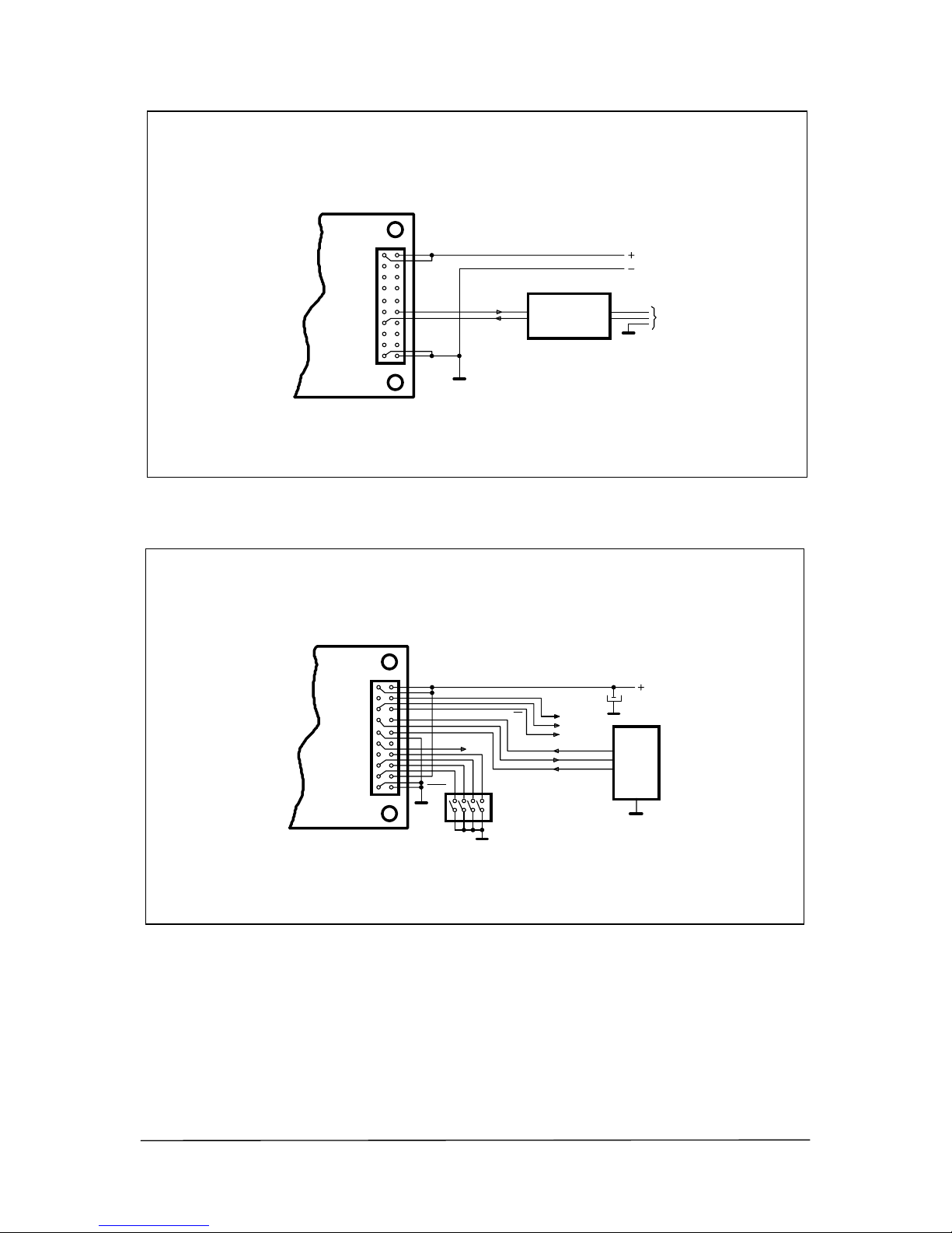
Fig. 8 Typical transceiver connections in “Voice” mode (analogue signals).
J1
2
1
3
5
7
9
11
13
15
17
19 20
5 VDC
4
6
MCU
PTT
RXD
TXD
CTS CHD
CHC
CHB
CHA
DATA/
VOICE
ARX
RSI
CD
J1
2
1
3
5
7
9
11
13
15
17
19 20
5 VDC
4
6"S"
RX AUDIO OUTPUT (245 mVrms)
CAR.DECT.
-10 dBm , 600 Ohm Load
ATX
CHD
CHC
CHB
CHA
ARX
RSI
CD
TX AUDIO INPUT (245 mVrms)
-10 dBm , 600 Ohm Load
NOTE (1) : S3 SELECTOR = OPEN
PTT
(1)

STE sas Milano - ITALY Pag. 8 of 14
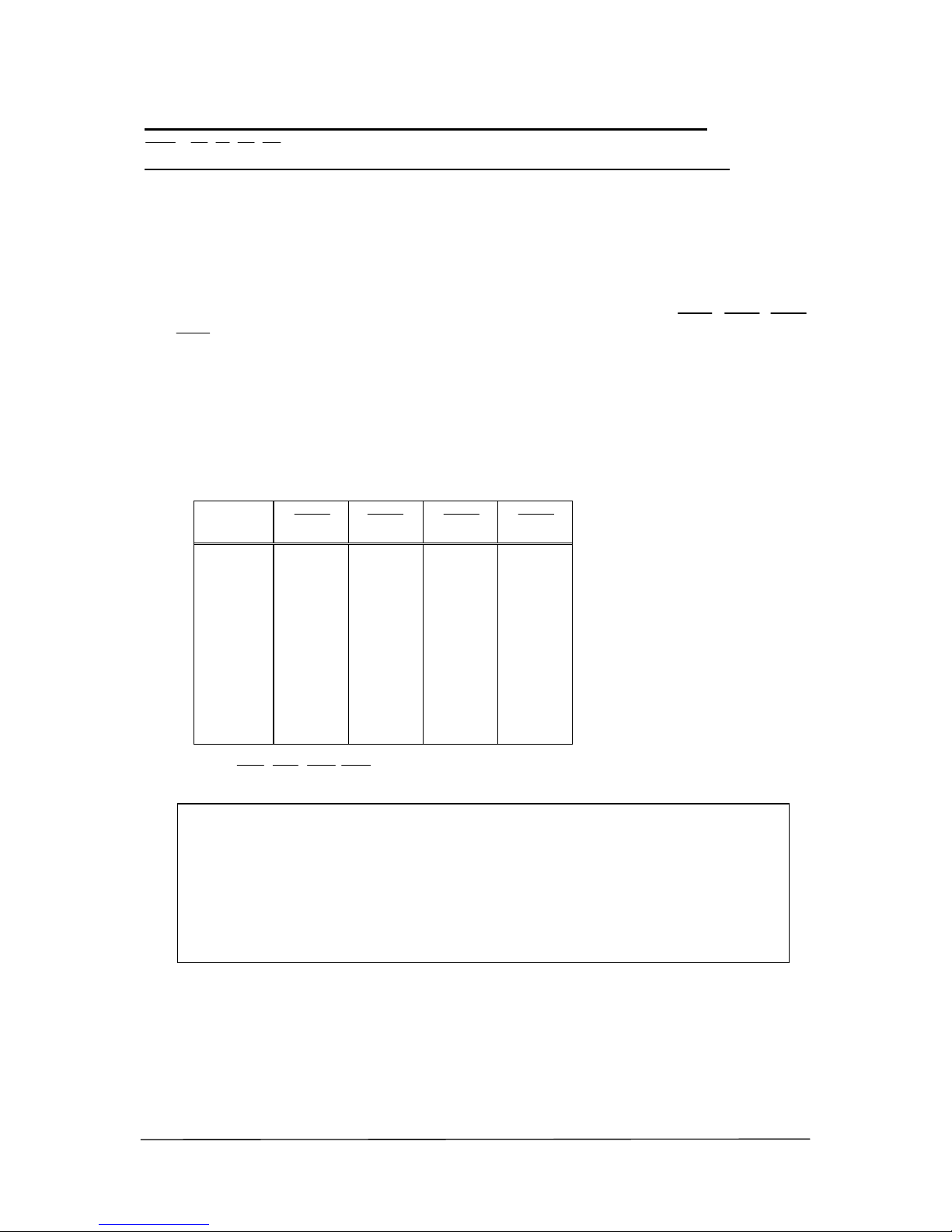
Fig. 9 Transceiver total control ( “DATA” mode) by external host microcontroller (TX , RX,
frequency, power ).
J1
2
1
3
5
7
9
11
13
15
17
19 20
4
6
MCU
RXD
TXD
TX
RX
DATA/
VOICE
ARX (MONITOR)
RSI ("S")
CD (CAR. DET.)
5 VDC
PRO
PRI UART

STE sas Milano - ITALY Pag. 9 of 14
DATA/VOICE input ( D/V - J1 pin n.18 )
The transceiver has two main operating modes, depending on D/V input :
1) D/V = Low ( 0 V )
“Voice” (analogue) signals can be transmitted with narrow band frequency modulation
(NBFM).
Depending on the selectors S2 and S4 (“A” or “B” position), PM (phase modulation
with 6 dB/oct emphasis) or FM (frequency modulation with flat frequency deviation) can
be selected.
Note : During “Voice” operating mode the Tx data input (TXD) is disabled .
2) D/V = High ( 5 V ).
Digital Data can be transmitted ( max data rate = 9600 Baud ) and the modulation
system is changed to “GMSK”.
The transceiver employs a Two Point Modulation system (VCO plus PLL Reference
Oscillator – see block diagram Fig. 2 ) to provide a flat response from 4.8 KHz down to
DC.
Note : In “DATA” operating mode the TX “VOICE” analog input “ATX” (J1- pin n.9) is not disabled.
Signal on “ATX” input must be avoided.
P
M , with an optimum audio response from 300 Hz to 3KHz, is best suited for voice or telephone grad
e
s
ignals (DTMF, AFSK slow speed Modems, selective call, etc.) and has the best “S/N” ratio with an Rx
sensitivity of - 120 dBm ( 12 dB SINAD ).
FM with 3 KHz fixed deviation can be the best choice for audio signals ranging from 50 Hz to 5 KHz
(Fast Modems, V/F converters, etc.).
Receiver sensitivity is –110 dBm ( 12 dB S/N ).
During “DATA” operating mode the TX has only two discrete transmitted frequencies :
Bit “0” (“TXD” input= 5V) corresponds to a transmitted frequency FL= Fc – 3KHz
Bit “1”(“TXD” input = 0V) corresponds to a transmitted frequency FH = Fc +3KHz
(Fc is the nominal RF channel center frequency).
STE sas Milano - ITALY Pag. 10 of 14
PRO, PRI ( J1 pins n.12-13) programming input-output
CH A-B-C-D ( J1 pins n.14-15-16-17) channel select input
PRI and PRO are connected to the IC10 microcontroller USART input-output
( see block diagram Fig.2 ) and are used to program the transmit and receive frequencies and
the TX output RF power ( “High” or “Low” ).
Refer to Fig.5 for the programming set-up.
Sixteen channels can be programmed and stored in the IC10 EEPROM memory.
In operation one of the 16 channels is selected using parallel control lines CHA, CHB, CHC
and CHD ( negative logic).
The transceiver can be also programmed (Through PRI and PRO) during normal operation on
default channel n.1 .Serial mode programming software is available for the BK7XX
transceiver – for further details contact the STE sales office.
TABLE 1
CHANNEL
CHD
CHC
CHB
CHA
1 1 1 1 1
2 1 1 1 0
3 1 1 0 1
4 1 1 0 0
“ “ “ “ “
“ “ “ “ “
15 0 0 0 1
16 0 0 0 0
Note : CHA-CHB-CHC-CHD inputs have internal pull-up (10 KΩ) to + 5 V.
IC10 (see Fig. 2) is a PIC16F870 flash microcontroller whose function is to control the genera
l
f
unctions of the transceiver and to program the channel frequency ( transmit or receive ) in the
“PLL” integrated circuit ( IC11 –Fujitsu MB15E03SL ).
The microcontroller has inside an EEPROM where are stored program configurations for up to 1
6
channels ( transmit and receive frequency, in 12.5 KHz step , and RF output power ).
One of these 16 channels is selected using parallel control lines via the terminals CHA,CHB,CHC
and CHD of J1 connector

STE sas Milano - ITALY Pag. 11 of 14
BK77x FREQUENCY-POWER PROGRAMMING
At “Power On” the radio memory ( IC10 EEPROM ) is loaded with the “ DEFAULT “
channels ( see Table 2 ).
The radio can be programmed on different RF channels ( TX frequency , RX frequency and
TX output power level ) via “PRI” and “PRO” terminals ( J1 connector ) connected to the
serial “COM ” port of a “PC”.
“PRI” and “PRO” pins must be connected respectively to the “TD” and “RD” lines of the
RS232 port with a suitable “TTL” to “RS232” driver ( fig. 10 ).
Data are exchanged between the radio and the “PC” as “ASCII” characters : programs such
as “HyperTerminal” can be used to send and receive the “ASCII” strings of characters.
Serial protocol format : 9600 Baud , 8 data bit , 1 stop , no parity .
Fig . 10 PC/RADIO programming with TTL/RS232 driver.
Each channel can be individually programmed on new frequencies ( and RF power level ) :
the new data will be retained into the radio memory (EEPROM).
At any time, if necessary, a “RESET” command reloads the memory with the “DEFAULT”
channels.
J1
2
1
3
5
7
9
11
13
15
17
19
12
20
PC PORT
GND
RS232
PRO
PRI
5 VDC
4,7K
10K
BC547
1N4148
10K
4,7K
4,7K BC557
220
220
2,2K
22uF
-10 V
1N4148
TTL/RS232 DRIVER
RD
TD
GND
2
3
5
16V
47uF
10V
BK7XX

STE sas Milano - ITALY Pag. 12 of 14
PROGRAMMING COMMANDS AND PARAMETERS
[ CH ] WRITES IN “EEPROM” TX FREQUENCY, TX POWER LEVEL
( HIGH, LOW ) AND RX FREQUENCY.
FORMAT : CH ( § , &&&& , $$$$ ) [ CR ] [ LF ]
§ = CHANNEL NUMBER ( HEX FORMAT, FROM 0 TO F)
& = 4 HEX DIGITS , “ NT” NUMBER.
$ = 4 HEX DIGITS , “ RT” NUMBER.
[CR]= CARRIAGE RETURN ( ASCII CODE 0D)
[LF] = LINE FEED ( ASCII CODE 0A)
[ RESET ] GENERAL RESET WITH “EEPROM” RELOADED WITH
“DEFAULT” CHANNELS
FORMAT : RESET [ CR ] [ LF ]
[ # ] DATA REQUEST
FORMAT : # [ CR ] [ LF ]
AT RECEPTION OF “ # “ COMMAND , THE RADIO ANSWERS
BACK THE ACTUAL PROGRAMMED DATA AND OPERATION
MODE.
ASWER FORMAT : # αβ§ XXXX [ CR ] [ LF ]
α= RADIO STATUS ( T = TRANSMISSION, R= RECEPTION )
β= RADIO MODE ( V = VOICE, D = DATA )
§ = SELECTED CHANNEL ( HEX FORMAT , 0 TO F )
X = 4 HEX DIGITS , “ NT” OR “ RT” NUMBER.
[CR]= CARRIAGE RETURN ( ASCII CODE 0D)
[LF] = LINE FEED ( ASCII CODE 0A)
NOTES :
1) Characters must be sent as written : capital letters, Hex numbers, commas and round
brackets.
2) A two seconds “Time-Out” is active between character typing.
3) In case of error or “Time-out” the radio answer-back “ ? ” character.
4) The 16 channels are numbered 1-16 (see table 1). When programmed with “CH”
command channels must be entered as hexadecimal number from “0” to “F”.
5) [ CR ] and [ LF ] (if correctly configured into “HyperTerminal program) are
automatically sent by pressing “ ENTER “.

STE sas Milano - ITALY Pag. 13 of 14
NT and NR number calculation ( BK 77x )
“NT” and “ NR” are 16 bit binary numbers used to program the “PLL” N-divider in TX
and in RX mode.
“NT” and “NR” are entered into the radio in hexadecimal format. The “MSB” bit of “NT”
is used as a flag to program the RF output power : 1 = HIGH POWER , 0 = LOW POWER.
“NT” is calculated dividing the required TX frequency (KHz) by 12.5 ( 12.5 KHz
is the frequency programming step ).
“NR” is calculated from the required RX frequency (KHz) subtracting 21400
(21400 KHz is the first conversion intermediate frequency ) and then dividing by
12.5.
The “PLL” IC ( a FUJITSU MB15E03) when programmed for 64/65 prescaler
divide ratio, has an internal register ( “N” register ) where bit n° 6 of “N” word
must be set to 0 and ignored. To do this a 0 bit must be inserted as n° 6 bit into the
calculated “NT” and “NR” binary numbers.
A) “NT” calculation :
1) nT number : nT = TX FREQ.( KHz ) / 12.5
2) Write down nT in binary format ( 16 bit ).
3) Insert a 0 into nT as bit n° 6.
4) Write down the new binary number and eliminate the “MSB”
5) Convert in Hexadecimal format.
6) For “HIGH POWER” the MSB bit of the first Hex number must be set to “1”.
B) “NR” calculation :
1) nR number : nR = [ RX FREQ.(KHz) - 21400 ] / 12.5
2) Repeat point 2 to 5 as above.
EXAMPLE :
A) TX FREQ. = 433.7125 MHz
nT NUMBER = 34697 = 8789 H = 1000 0111 1000 1001
New bin. Number with 0 at n° 6 bit = 10000 1111 0000 1001
NT NUMBER ( LOW POWER) = 0000 1111 0000 1001 = 0F09 H
NT NUMBER ( HIGH POWER) = 1000 1111 0000 1001 = 8F09 H
B) RX FREQ. = 433.7125 MHz
nR NUMBER = 32985 = 80D9 H = 1000 0000 1101 1001
New bin. Number with 0 at n° 6 bit = 10000 0001 1001 1001
NR NUMBER = 0000 0001 1001 1001 = 0199 H
“CH” command format to program channel n° 2 on 433.7125 MHz ( transmit and
receive) , high power :
CH ( 1,8F09,0199 ) [ CR ] [ LF ]

STE sas Milano - ITALY Pag. 14 of 14
TABLE 2
BK77x DEFAULT CHANNELS
CH.
N°
CH.
HEX
FREQ.
MHz
POWER
LEVEL
“ NT ” “ NR “
1 0 433.2125 L 0EA1 0131
2 1 433.2375 L 0EA3 0133
3 2 433.2625 L 0EA5 0135
4 3 433.2875 L 0EA7 0137
5 4 433.3125 L 0EA9 0139
6 5 433.3375 L 0EAB 013B
7 6 433.3625 L 0EAD 013D
8 7 433.3875 L 0EAF 013F
9 8 434.3125 L 0F39 0209
10 9 434.3375 L 0F3B 020B
11 A 434.3625 L 0F3D 020D
12 B 434.3875 L 0F3F 020F
13 C 434.4125 L 0F81 0211
14 D 434.4375 L 0F83 0213
15 E 434.4625 L 0F85 0215
16 F 434.4875 L 0F87 0217
Table of contents


