20-Jun.2017 Ver.1.3
TAIYO YUDEN CO., LTD.
TAIYO YUDEN CO., LTD. 8/16
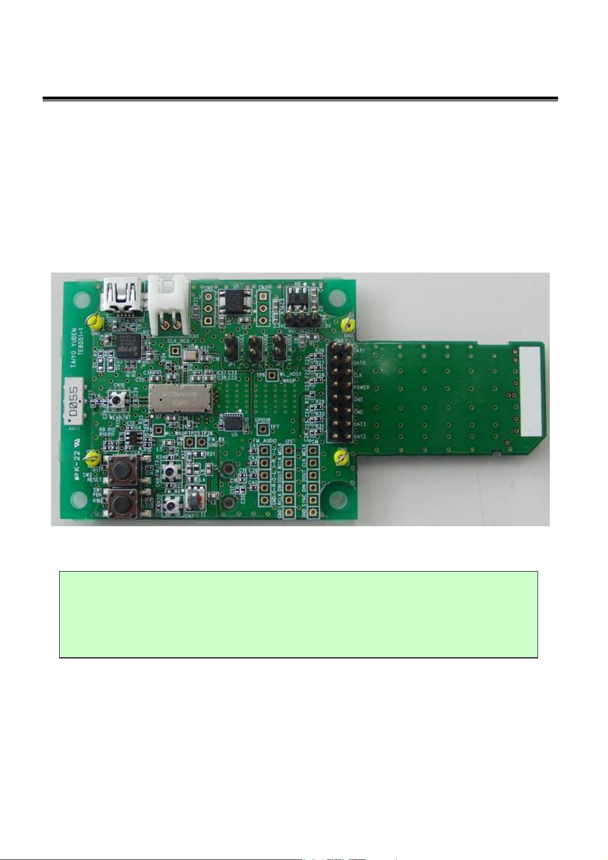
WBSBMVGXB-1
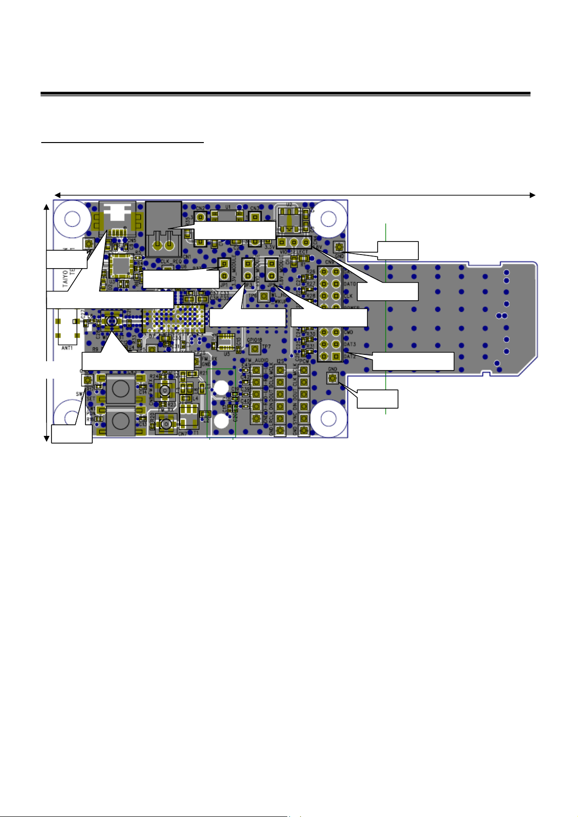
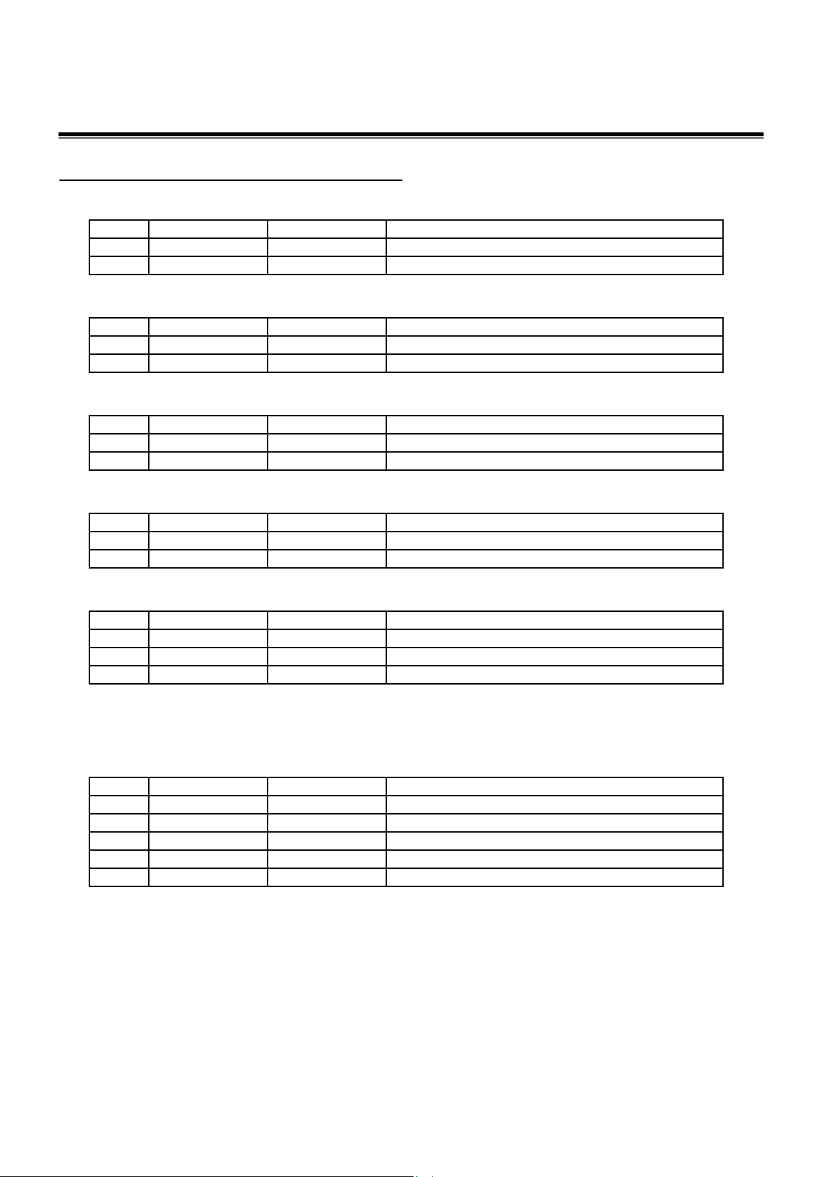
Pin description of evaluation board
JP1: 3.3V to module
No. Pin name Direction Description
1 Output 3.3V output
2 input 3.3V input to the module
JP2: 1.8V to module
No. Pin name Direction Description
1 Output 1.8V LDO output
2 input 1.8V input to the module
JP3: VIO to module
No. Pin name Direction Description
1 Output 3.3V or 1.8V output
2 input VIO Input to the module
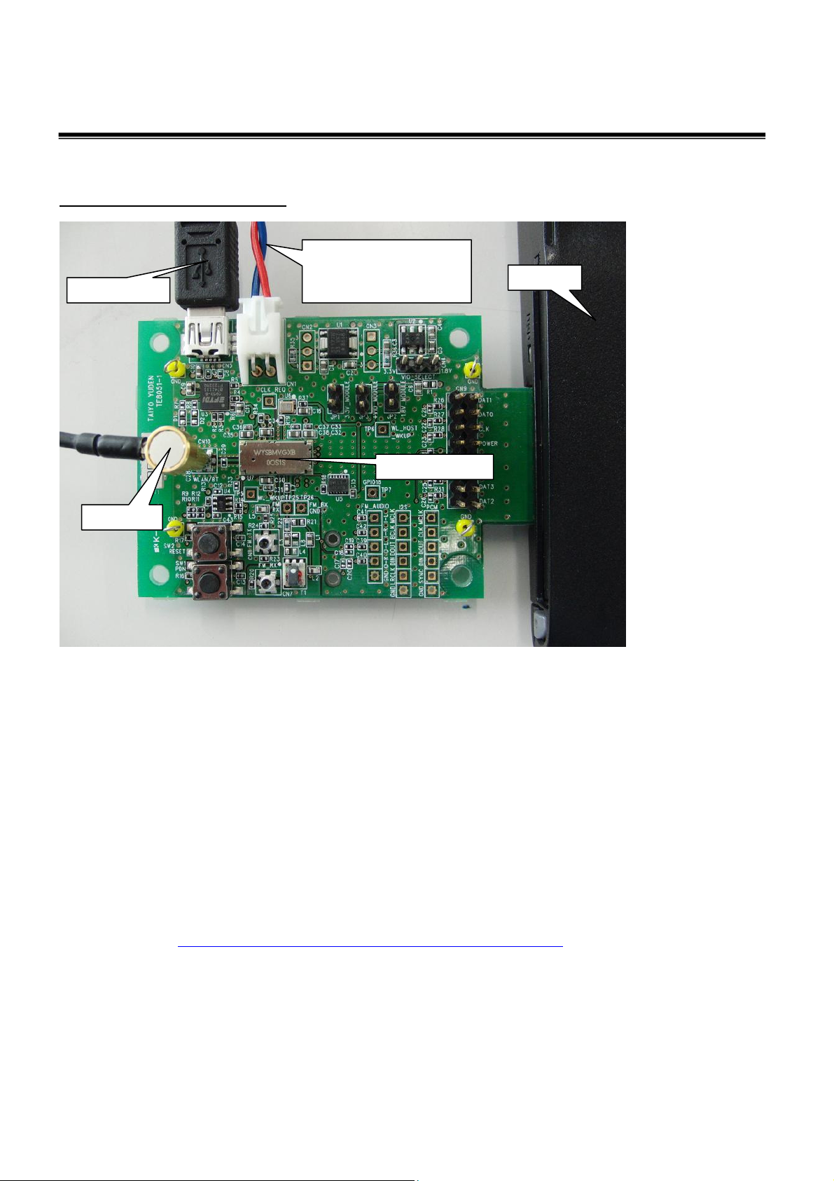
CN1: DC Power Supply
No. Pin name Direction Description
1 5V Input 3.6 to 5.5V DC Power input.
2 GND - VIO Input to the module
CN4:VIO select (1.8V / 3.3V)
No. Pin name Direction Description
1 Output 3.3V power rail
2 Input Input power to VIO
3 Output 1.8V power rail
Note: VIO input voltage level should be same as HOST computer’s IO voltage. According to the host,
you need to adjust VIO input voltage level. (If you use Windows PC, VIO input setting is 3.3V
normally.)
CN5:USB mini type B connector
No. Pin name Direction Description
1 VBUS Input USB power from host
2 D- Input/Output USB data line minus
3 D+ Input/Output USB data line plus
4 ID - -
5 GND - Ground