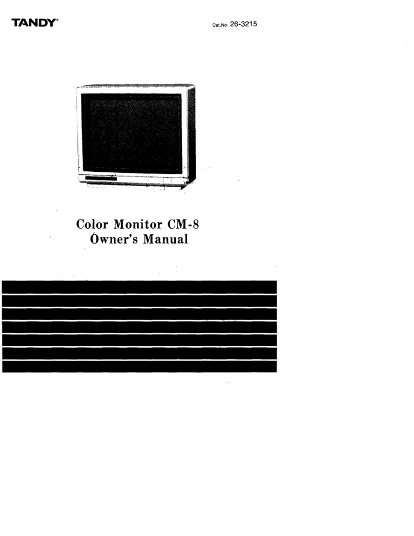
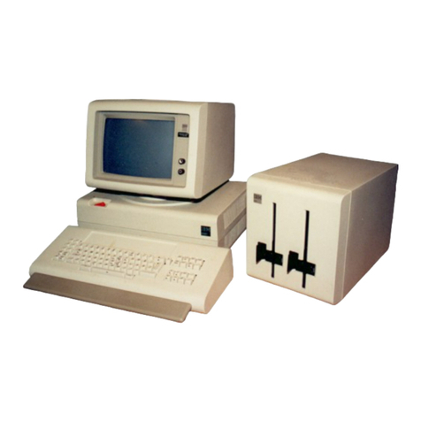
Tandy CM-4 User manual

TANDY8
Service
g^^s^--" rv;i-; '^W-?-K'^ :'- s^'^^<-:
''
:'-^'^^^^V :^^^ ^'^^P^h^' '> S'V-r^ *''.',' ;'' '
:--"v-"- -.-^. ^yrtj^^^-'ix ,f~.- &-.%• r&tnzi
^iii^Ss^^sSi
COLOR MONITOR
CM-4
Catalog Number :25-1021
Iks
i
fe2
^^?^'v*8i5$S>!^^ "''" *" ,""x"* '". .:.. :""'."

CONTENTS
Page
SPECIFICATIONS 3
IMPORTANT SERVICE SAFETY PRECAUTIONS 4
THEORY OF OPERATION 6
DISASSEMBLY INSTRUCTIONS 12
BLOCK DIAGRAM 13
ALIGNMENT INSTRUCTIONS 14
TROUBLESHOOTING GUIDE 18
P.C. BOARD (Top and Bottom Views)
CRT Socket PCB 22
LED PCB 23
Main PCB 23
WIRING DIAGRAM AND PARTS LOCATION 27
CABINET EXPLODED VIEW/PARTS LIST
1. Cabinet Exploded View 28
2. Electrical Parts List 29
3. Cabinet Parts List 39
SCHEMATIC DIAGRAM 41
WAVEFORMS 44
SEMICONDUCTOR LEAD IDENTIFICATION 44

SPECIFICATIONS
Description Nominal Limit
1. Power input AC 120V, 60Hz
2. AC input current 0.75A +10%
-30%
3. Input signal
a) RGB Video RGB separate T.T.L.
Level, positive white
2.4 -5.0Vp-p
~^"~ (default)
b) Synchronous "
"T.T.L. level, positive going
(default)
c) Intensity T.T.L. level, positive going
(default)
4. Resolution
a) Horizontal 640 dots
b) Vertical (non-interlaced) 225 lines
6. Brightness 30 fl. min. (at intensity
white)
8. Display color 15colors
9. High voltage 23 kV/O^A 27.5 kV maxJOfJK
10. Picture linearity
a) Horizontal 10% max.
b) Vertical 10% max.
11. Synchronous (Pull in range)
a) Horizontal 15.701 kHz :i>
b) Vertical 60 Hz >
12. Dot Pitch 0.64 mm
NOTE:
Nominal specs represent the design specs; all units should be able to approximate these —some will exceed
and some may drop slightly below these specs. Limit specs represent the absolute worst condition which still
might be considered acceptable; in no case should aunit perform to less than within any limit spec.

IMPORTANT SERVICE SAFETY PRECAUTIONS
Service work should be performed only by qualified service technicians who are thoroughly familiar with all of
the following safety checks and servicing guidelines:
WARNING
1. For continued safety, do not attempt to modify the
circuit.
2. Disconnect the AC power before servicing.
3. Semiconductor heat sinks are potential shock haz-
ards when the chassis is operating.
SERVICING THE HIGH VOLTAGE SYSTEM
AND PICTURE TUBE
When servicing the high voltage system, remove the
static charge by connecting a10k ohm resistor in
series with an insulated wire (such as atest probe)
between the chassis and the anode lead. (The AC line
cord should be disconnected from the AC outlet.)
1. The picture tube in this display monitor employs in-
tegral implosion protection.
2. Replace with atube of the same type number for
continued safety.
3. Do not lift the picture tube by the neck.
4. Handle the picture tube only when wearing shatter-
proof goggles and after discharging the high vol-
tage anode completely.
X-RADIATION AND HIGH VOLTAGE LIMITS
1. Be sure all service personnel are aware of the
procedures and instructions covering X-radiation.
The only potential source of X-ray in acurrent solid-
state display monitor is the picture tube. However,
the picture tube does not emit measurable X-ray
radiation if the high voltage is as specified in the
"high-voltage check" instructions.
It is only when high voltage is excessive that X-
radiation is capable of penetrating the shell of the
picture tube, including the lead in glass material.
The important precaution is to keep the high vol-
tage below the maximum level specified.
2. It is essential that servicemen have available at all
times an accurate high voltage meter. The calibra-
tion of this meter should be checked periodically.
3. High voltage should always be kept at the rated
value —no higher. Operation at higher voltages
may cause afailure of the picture tube or high vol-
tage circuitry and, also, under certain conditions,
may produce radiation in excess of desirable levels.
4. When the high voltage regulator is operating proper-
ly there is no possibility of an X-radiation problem.
Every time acolor chassis is serviced, the bright-
ness should be tested while monitoring the high vol-
tage with ameter to be certain that the high voltage
does not exceed the specified value and that it is
regulating correctly.
5. Do not use apicture tube other than that specified
or make unrecommended circuit modifications to
the high voltage circuitry.
6. When troubleshooting and taking test measure-
ments on adisplay monitor with excessive high vol-
tage, avoid being unnecessarily close to the display
monitor. Do not operate the display monitor longer
than is necessary to locate the cause of excessive
voltage.
BEFORE RETURNING THE DISPLAY MONITOR
Fire and Shock Hazard
Before returning the display monitor to the user, per-
form the following safety checks:
1. Inspect all lead dress to make certain that the leads
are not pinched or that hardware is not lodged be-
tween the chassis and other metal parts in the dis-
play monitor.
2. Inspect all protective devices such as nonmetallic
control knobs, insulating materials, cabinet backs,
adjustment and compartment covers or shield, iso-
lation resistor-capacitor networks, mechanical in-
sulators, etc.
3. To be sure that no shock hazard exists, check for
leakage current in the following manner:
•Plug the AC line cord directly into an 120 volt AC
outlet. (Do not use an isolation transformer for this
test.)
•Using two clip leads, connect a 1.5k ohm, 10 watt
resistor paralleled by a0.15/iF capacitor in series
with all exposed metal cabinet parts and aknown
earth ground, such as electrical conduit or electri-
cal ground connected to earth ground.
•Use aSSVM or VOM with 1000 ohms per-volt or
higher sensitivity to measure the AC voltage drop
across the resistor. (See Figure 1.)

•Connect the resistor connection to all exposed
metal parts having areturn path to the chassis
(metal cabinet, screw heads, knobs and control
shafts, escutcheon, etc.) and measure the AC vol-
tage drop across the resistor.
All checks must be repeated with the AC line cord
plug connection reversed. (If necessary, anon-
polarized adapter plug must be used only for the pur-
pose of completing these checks.)
Any reading of 0.3 volt RMS (this corresponds to
0.2 milliamp. AC.) or more is excessive and indi-
cates apotential shock hazard which must be cor-
rected before returning the display monitor to the
user.
SAFETY NOTICE
Many electrical and mechanical parts in display moni-
tors have special safety-related characteristics. These
characteristics often pass unnoticed and the protec-
tion afforded by them cannot necessarily be obtained
by using replacement components rated for higher vol-
tage, wattage, etc.
Replacement parts that have these special safety
characteristics are identified in this manual; electrical
components having such features are identified by a
Aand shaded in the Replacement Parts Lists and
Schematic Diagram. For continued protection, replace-
ment parts must be identical to those used in the origi-
nal circuit. The use of asubstitute replacement part
that does not have the same safety characteristics as
specified in this service manual, may create shock, fire,
X-radiation or other hazards.
TO EXPOSED
METAL PARTS
CONNECT TO
KNOWN EARTH
GROUND
Figure 1. Leakage Current Test Circuit

THEORY OF OPERATION
1. RGB Drive Circuit
The RGBI signals are applied to HEX inverter IC491
used as abuffer). The outputs of IC491 are then ap-
alied to IC492 which is an open collector HEX invert-
er. The resistors tied to the outputs of IC492 are used
:o set the appropriate voltage level for the color sig-
nals. The signals are then applied to the base of RGB-
Amp transistors Q451, Q461 and Q471.
The brightness and sub brightness controls (R41 7and
341 6) are used to adjust the bias of the RGB-Amp tran-
sistors. These controls are connected to the base of
Q401 and Q402. When the intensity signal is LOW,
transistor Q421 is turned ON.
The contrast control (R422) is used to adjust the con-
trast between high and low intensity color signals.
2. Video (RGB) Output {Fig. 2)
An RGB drive system is utilized in the video output cir-
cuit of this unit. The function of this circuit is to com-
oine the color signals and the brightness signal, and
amplify them sufficiently to drive the cathodes. 145V
DC must be applied to the collectors of the output tran-
sistors (Q851, Q861, Q871). When the horizontal
output circuit is operating, pulses are developed and
fed to the 116V supply where they are applied to a
winding of the horizontal output transformer (T602).
This pulsed DC voltage is then taken from terminal (s)
of T602 and applied through D71 7, and R865 or R866
or R867 to the collectors of Q851, Q861 andQ871,
respectively.
The brightness signal from the Blanking (Q402) is ap-
plied to the emitters of Q851, Q861 and Q871.
C853 and C855 are peaking capacitors.
Color signals from the outputs of Q451, Q461 and
Q471 are applied to the bases of Q851, Q861 and
Q871 .The picture tube used in this unit is aprecision,
inline gun-type. The control grid (G1) and the screen
grid (G2) are common with respect to the red, green
and blue cathodes. Consequently, the emitter circuits
of Q85 1,Q86 1and Q87 1are provided with bias con-
trols (R862, R863 and R864, respectively) for picture
tube cut-off adjustment. Drive controls (R856 and
R858) are provided in the emitter circuits of Q851 and
Q871 for white balance adjustment.
FROM
EMITTER >
OF Q451
Q851
RED OUTPUT
FROM
EMITTER >
OFQ461
FROM
EMITTER >
OFQ471
FROM
VIDEO DRIVE >
CIRCUIT
<+145
Figure 2. Video Output Circuit

3, Vertical Deflection Circuit
The vertical sync, signal with positive polarity is ap-
plied to pin(7)of the vertical and horizontal IC (IC601).
Pin (8)of IC601 is connected to the vertical oscillator
circuit. The frequency of the oscillator can be con-
trolled by the voltage of pin (8) which can be varied
by V.HOLD VR (R514). The sawtooth signal is ob-
tained by the integrating circuit which is connected be-
tween pin (5) and pin Qj) .
The oscillator output is fed to the vertical drive circuit
through abuffer circuit. Its output, derived from pin
(2) ,is applied to the vertical output.
The sawtooth wave is applied to pin (3) of IC601 as
an AC feedback signal.
The emitter circuit of Q501 is controlled by V-SIZE VR
(R507) to vary the vertical size of the raster.
The vertical linearity control (R526) is part of an in-
tegrating circuit which controls the sawtooth
waveform.
4. Horizontal Oscillator, AFC and Drive Circuit
The horizontal sync, signal with positive polarity is ap-
plied to pin (15) of IC601.
The output from the fly-back transformer (T602) is in-
tegrated and connected to pin (^3) of IC601 as part
of the automatic frequency control circuit.
H. CENT control (R623) determines the relative posi-
tion of the raster and picture.
The horizontal oscillation frequency can be controlled
by H. HOLD VR R607 connected to pin (j~2).
The horizontal frequency is obtained from pin \[Q) of
IC601, and is fed to the next horizontal drive circuit.
The pulse-switching mode of the driver and output
stage is areverse polarity type; that is, when the driver
transistor Q601 is ON, the output transistor Q602 is
OFF.
5. Horizontal Output and HV Rectifier
(Figs. 3-5)
Horizontal drive voltage, developed at pin ^6) of the
deflection processor integrated circuit (IC601 ), is am-
plified through the horizontal drive stage (Q601) and
coupled to the base of the horizontal output circuit via
the horizontal drive transformer (T601 ). Refer to Fig. 3.
The horizontal output circuit generates the horizontal
scan and high voltage to be applied to the picture tube.
The function of the horizontal output stage (Q602) is
to serve as aswitch for the horizontal output circuit.
Refer to Fig. 4.
During the horizontal scanning period, Qoperates (S
1
is closed, S2 is open) and the current is applied in one
direction through the horizontal coils of the deflection
yoke (LY) and the capacitor (C). During retrace time,
Qis inoperative (S 1is open, S2 is closed) and the cur-
rent is applied in the opposite direction through the
damper diode (D), the horizontal coils of the deflection
yoke (LY) and the capacitor (C).
The high voltage required to be applied to the anode
of the picture tube is generated by boosting the pulse
from the collector of Q602 through T602 during the
flyback (retrace) period and applying this boosted pulse
to aseries of silicon rectifiers. Refer to Figure 5.
High voltage regulation is accomplished internally in
T602.
T601
HORIZ. DRIVE
From Pin (TS) ^
of IC601 ^
C609 T
I
To BASE
of Q602
Q601
HORIZ. DRIVE ^+12V
Figure 3. Horizontal Drive Circuit

Q(S1)
~© 1
DAMPER
DIODE (S2)T Cr'COIL)
LY
(DEFLECTION
VCC
(A) (B)
Figure 4. Equivalent Circuit of Horizontal Output Circuit
I—''—IR71
18V «•*H*>W
C72izt °714 R717 ^T
TO CRT
SECOND ANODE
** TO CRT FOCUS
*- TO CRT SCREEN
** TO ABL CIRCUIT
145V
To Blanking and
orizontal
AFC DET. Circuit
*• TO CRT Heater
(THIS AREA IS COLD GROUND)
D713
AAV- p\—f18V
Figure 5. Horizontal Output and HV Rectifier Circuit

6. High Voltage Shut-down System
The shut-down circuit prevents the high voltage from
rising above apreset level.
Under normal operating conditions, this circuit is in-
active.
Operation of the protector circuit depends upon aheat-
er pulse which appears at pin {3) of the horizontal out-
put transformer (T602). It monitors aheater pulse
subjected to rectification by D603. Being in proportion
to the voltage of that heater pulse, if the incoming
high voltage increases and exceeds its limit, the heat-
er pulse voltage also increases. As aresult, there is
alarger voltage produced to charge C617 so that its
potential will eventually be higher than the voltage
(+22V) of Zener diode (D605) turning it ON. With
D605 turned ON, the X-ray protector (of IC601 )oper-
ates to stop the horizontal oscillator circuit, shutting
down the resultant high voltage.
FROM PIN©
OF T602
/HEATER \
\pulse ;
>R615 D603
-w M— D605 R618
—^VA-
R619? ±ZZC617 R6175 -^
77T
Figure 6. High Voltage Shut-Down System Circuit
R616 ^
-AW-(V)
C607
7. Power Supply (Figs. 7—10)
The entire monitor circuitry is protected by a4.0A fuse
(F701), located on the Main Chassis Board (PCB-A)
that is connected to the hot side of the AC line input.
The secondary circuit is protected by a1.5A fuse
(F702), mounted on PCB-A. AC Line voltage is applied
through the Line filter (L702) to the power ON-OFF
SWITCH (SW701).
With SW701 set in the ON position, AC voltage is ap-
plied through aBridge Rectifier circuit.
Aconventional type Automatic Degaussing circuit,
consisting of apositive coefficient thermistor (PR701
)
in series with the degaussing coil assembly (L701 ), is
used.
The AC input voltage is rectified by the Bridge Rectifi-
er circuit (D701 ,D702, D703, D704) and then applied
to the Regulator circuit. Aswitching type Regulator cir-
cuit, utilizing asilicon controlled rectifier (SCR701), is
used to maintain aconstant DC voltage level regard-
less of fluctuations \n the AC input voltage.
The negative horizontal pulses that are produced at ter-
minal @of the Horizontal Output transformer (T602)
are converted into asaw tooth wave by R713 and
C71 1which is applied to the Phase Detector circuit
in the IC701 (Power Regulator integrated circuit) via
pin (5) .Output from the Phase Detector circuit is ap-
plied internally to the SCR Drive stage where it is am-
plified and then utilized as the SCR gate (timing) pulse.
Gate pulse timing is determined by the action of the
Error Amplifier stage in IC701 which is controlled by
the setting of the +116V Adjust control (R707).
Filtered DC voltage derived from the pulses produced
at terminals @and @of T602 is used to turn OFF
SCR701. If the AC input voltage increases, the turn-
on time of SCR 701 decreases. And if the AC input
voltage decreases; the turn-on time of SCR701 in-
creases.
The +5. 1V, +12V and +18V supplies are produced
as aresult of rectification through D71 3of the pulses
developed at terminal @of T602.

R631 D717
F701 L702 SW701 D701 ~D704
£-c5\p— LINE
FILTER
<rom-
AC120V
60Hz
F701
r\j )AC120V
w'60Hz
BRIDGE
RECTIFIER
r^V M»+145V
IC701
HORIZ.
OUTPUT
XFMR. REGULATOR
CIRCUIT
D714
T701
Power
Trans
JBridge
Recti-
fier
D708 Q701 R716 D713
-+12V
Regu-
lator R401
+116V
+18V
+12V
+5.1 V
R481
Figure 7. Block Diagram of Power Supply
PR701
-Cwv^
IL701
ADG
O
C
33
33
m
Figure 8. ADG Circuit
^
TIME
=ROM BRIDGE^ #/gj OUTPUT
RECTIFIER 'Tv^ ve„Dul
SCR
STARTER
HORIZ. 3)-
XFMR ^
3T ^SCR701
TO COLLECTOR OF-Q602
mm REGULATED
OUTPUT +116
r-<p-- —<£> 1
SCR
DRIVE
Ii i
PHASE
DETECTOR ERROR
AMP.
IREFERENCE
VOLTAGE
:F—--
REGULATOR
IC
(IC701)
r4>
Figure 9. Block Diagram of Regulator Circuit
10

AC120V
60Hz ^C716 /*+-
C714
+145V
D717
Figure 10. Power Supply Schematic

DISASSEMBLY INSTRUCTIONS
Remove the six screws (T) retaining the rear
cabinet.
Remove the rear cabinet. (Figure 11A)
Note: The CRT must be discharged. Refer to the
high voltage discharge procedure on page 4.
(1) Remove the CRT's second anode cap(2)from
the CRT.
(2) Remove the PCB--B (CRT PCS) lead of the CRT
grounding strap. (Figure 11B)
(3) Remove the PCB-B.
(4) Loosen the wire holder on the Flyback trans-
bracket and disconnect the connector K.
(Figure 11B)
(5) Disconnect the connectors NA and Mon the
PCB-A (main PCB-A)
(6) Loosen the wire holder fixing power switch
lead, CRT ground lead, RGB output lead,
Degaussing lead and LED lead. (Figure 11B)
(7) Remove the PCB-A (main PCB) from the front
cabinet.
3. Remove screw (5) for PCB-C the LED and also
PCB-C from the front cabinet. (Figure 11B)
Note: When servicing, be sufficiently careful with the
control door because it may detach from the
cabinet if it touches the surface while the set
is inclined toward the front.
Figure 11A
Figure 11B
12

BLOCK DIAGRAM
CO
w
£o
°h
o<
I- o
*44
CO
ox
uj
I- QLU co
<
CO
UJ
z
z-J Ncc
LU O»-i i- X
oxCO zo
ii1oCE
I> > oCD
o
UJ
Q
z
o<
^r _j
om
gUJCL
lO (£> NZjQJ-
00 CO 00 o•"•3
OOOo>o
hhJt
or
in co r- Sq^
*• ^<* ^i-iS
oooo><
m
I- ft Hi
°!5 °8or
J
CD
O
O<
orr
o
Li.
CO
o
o:
o
H
O
ffl
<i-t
q: LU 1-
>o
a: o
XFH rr
?or a.
<<C oV
o<> HH <
(0 zo: oc tr
C) VLU LU i
CO >>X
or
UJ
cm £
co tu .
•-i M <
>
ouj o
"* i- a
OZM
~wO
o:
uj
_t-
aj£ .
°z^
~M<
r
10 Z3
0> UJO
*" *-0E
OZh
•-WO
x5
.On
XQO
<
z
o
CM hi
coo
t-x
^1
NUJ
-_ M>
Oo o: w
co cd oor
Oh xa
CM
O
2»-
o.u
jhl
oox |-
io uj 2
o>o
xoe
UJ
h-
q:
uj
CM >
sz
CM
cm za:
** ow
ooo
/b ooo\ <»-
/o oooo\ Si
v'co M
>
CO >
CM
1
>
iri
+
x
00 c*
o
LU £.
Q£Q
UJ O Z
J0-H
13

ALIGNMENT INSTRUCTIONS
Mote:
This adjustment requires the connection of apersonal
computer to the Monitor. Although the Monitor is ad-
usted before it Is delivered, readjustment may be re-
quired when the setting position is changed or when
icomponent is replaced.
1. B+ Power Circuit Adjustment
(Instrument in use: a20 kohm/V tester)
1) Be sure that the AC line voltage is above 114V.
2) Rotate the B+voltage adjusting control (R707) to
provide aDC voltage of 116V between TP91 and
ground.
Mote 1:If the AC line voltage is below 114V, the
DC voltage may not increase to 116V, but
this is not aproblem related to this adjust-
ment. If the value of 116V DC is almost
reached, the adjustment is enough.
-Mote 2: Clockwise rotation of the B+ voltage ad-
justing control will increase the B+power
supply voltage.
2. Horizontal Hold Adjustment
(1) Operate the computer in such away that the let-
ters "H" cover the entire screen (data display peri-
od: 44.698 /*S horizontal, 14.33 mS vertical).
(2) Adjust the horizontal hold control (R607) until the
picture on the screen becomes still (synchronized).
(3) Turn the power switch on and off several times
to check that the picture does not fluctuate.
3. Vertical Size Adjustment
(1
)
Operate the computer in such away that the let-
ters "H" cover the entire screen (data display peri-
od: 44.698 mS horizontal, 14.33 mS vertical).
(2) Adjust the vertical size control (R507) so that the
height of the displayed pattern is 170 mm.
4. Focusing
(1) Operate the computer to display the alphabetical
characters on the screen.
(2) Set the brightness control at the center position.
(3) Rotate the focus adjusting control (part of T602)
for the best focus.
(4) Change the position of the brightness control to
confirm that the picture remains focused.
5. High Voltage Check
High voltage is not adjustable but must be checked to
verify that the Monitor is operating within safe and ef-
ficient design limitations as specified.
1
.
Operate the display Monitor for at least 15minutes
at 120VAC line voltage with the computer display-
ing high intensity white pattern.
2. Turn off Switch SW851 on PCB-B.
3. Rotate the screen control (on T602) to the maxi-
mum (counterclockwise) end of its rotation.
4. Connect an accurate, high-voltage meter to the
CRT anode. Check that the reading is approximate-
ly 22.0kV and 23.0kV (at beam current).
If acorrect reading cannot be obtained, check the cir-
cuitry for malfunctioning components. On completion
of the voltage check, readjust the screen control for
proper operation as detailed in the "Black and White
Tracking" procedures.
6. Vertical-Linearity Adjustment
1
.
Operate the computer in such away that the let-
ters "H" cover the entire screen (data display peri-
od: 44.698 /iS horizontal, 14.33 mS vertical).
2. Adjust the V-Lin. control (R526) until the height
of acharacter varies no more than 1percent from
the average character size.
7. X-ray Protector Circuit Test
After service has been performed on the horizontal
deflection system, the high voltage system and the X-
ray protector circuit must be tested for proper opera-
tion as follows:
1
.
Apply 120VAC, using avariac transformer for ac-
curate input voltage.
2. Operate the computer in such away that the en-
tire screen displays ahigh intensity white signal
(data display period: 44.698 /*S horizontal, 14.33
mS vertical).
3. Check the voltage of test point TP601 .(Its voltage
should be about 17.5VDC.)
4. Connect the cathode of diode D503 and TP601
through a6.8K ohm, 1/2W resistor.
5. To start operation, remove the resistor and touch
the IC601 (9) pin-to-chassis ground with ashort
clip lead. (Remove the short clip lead as soon as
the set operates again with anormal picture).
6. Connect the short-clip lead between TP602 and
chassis ground. When these points are connect-
ed, the operation of the horizontal osc. must stop.
7. To start operation, remove the short-clip lead when
the set begins operating again with anormal
picture.
8. If the operation of the horizontal osc. does not stop
in steps 4and 6, the circuit must be repaired be-
fore the set is returned to the customer.
14

8. Color Purity Adjustment
The display monitor must have been operating 15
minutes prior to this procedure, and with the faceplate
of the CRT at room temperature. The display monitor
is equipped with an automatic degaussing circuit.
However, if the CRT shadow mask has become exces-
sively magnetized, it may be necessary to degauss it
with amanual coil. Do not switch the coil off while
the raster shows any effect from the coil.
1
.
Check for the correct location of all neck compo-
nents. Refer to Figure 13.
2. Rough in the static convergence at the center of
the CRT, as explained in the static convergence
procedure.
3. Rotate the contrast control to the center of its
range and rotate the brightness control to its max-
imum clockwise position.
4. To obtain ablank raster, disconnect Efrom PCB-A.
Rotate the screen control (part of T602) clockwise
until anormal raster is obtained.
5. Rotate the red bias (R862) and blue bias (R864)
controls to the maximum counterclockwise po-
sitions.
Rotate the green bias control (R863) sufficiently
in aclockwise direction to produce agreen raster.
6. Loosen the deflection yoke clamp screw and pull
the deflection yoke as close as possible to the pu-
rity and convergence magnets assembly.
7. Begin the following adjustment with the tabs on
the round purity magnet rings set together. Initial-
ly, move the tabs on the round purity magnet rings
to the side of the CRT neck. Then, slowly separate
the two tabs while at the same time rotating them
to adjust for auniform green vertical band at the
center of the CRT screen. Refer to Figure 12.
8. Carefully slide the deflection yoke forward to
achieve green purity (uniform green screen).
Note:
Center purity is obtained by adjusting the tabs on
the round purity magnet rings. Outer edge purity
is obtained by sliding the deflection yoke forward.
Tighten the deflection yoke clamp screw.
9. Check for red and blue-field purity by reducing the
output of the green bias control (R863) and alter-
nately increasing the output of the red (R862) and
blue (R864) bias controls, and touch up the ad-
justment, if required.
10. Reconnect Eto RCB-A.
11. Perform the "Black and White Tracking"
procedures.
DEFLECTION YOKE
CLAMP SCREW
GREEN RASTER
Figure 12. Color Purity Adjustment
rPURITY MAGNETS
FOUR-POLE CONV. MAGNETS
SIX-POLE, CONV. MAGNETS
45.9mm
(1.807 inches)
DEFLECTION
YOKE
DEFLECTION YOKE TILT
ADJUSTMENT WEDGE
Figure 13. Picture Tube Neck Components Location
15

9. Black and White Tracking
1
.
Turn the screen control fully clockwise. Turn the
red, green and blue bias controls fully clockwise.
Set the brightness control and the red and blue
drive controls at the center positions.
2. Operate the computer in such away that the en-
tire screen is high intensity white (display period:
44.698 fiS horizontal, 14.33 mS vertical).
3. Turn off the switch SW851
.
4. Rotate the screen control counterclockwise until
araster (either the red, green or blue) appears dimly
on the screen.
5. Rotate two of the three bias controls counterclock-
wise until the raster becomes whitish: position ro-
tated controls must be the ones which control the
colors other than the raster's colors.
Notes: Adjust R863 and R864 if the red appears.
Adjust R862 and R864 if the green appears.
Adjust R862 and R863 if the blue appears.
6. Return switch SW851 to its original position.
7. Rotate the red and blue drive controls until the
raster is white.
8. Set the brightness control at its maximum position
and adjust the screen control until areading of
3.8V DC appears between TP-402 and TP-403 (at
both ends of R407).
9. Turn the brightness control in either direction to
check that the picture maintains agood white
balance.
10. Repeat steps 3thru 9for readjustment.
10. Static (Center) Convergence
(Figs. 13-16)
1. Switch the display monitor ON and allow it to
warm up 15 minutes.
2. Operate the computer in such away that the en-
tire screen is aCrosshatch pattern (display period:
44.698 fiS horizontal, 14.33 mS vertical) on the
center of the CRT screen. (Fig. 14)
Proceed as follows:
a. Locate the pair of four-pole magnet rings. Ro-
tate the individual rings (change spacing be-
tween tabs) to converge the vertical red and
blue lines. Rotate the pair of rings (maintaining
spacing between tabs) to converge the horizon-
tal red and blue lines. Refer to Figure 15.
b. After completing red and blue center conver-
gence, locate the pair of six-pole magnet rings.
Rotate the individual rings (change spacing be-
tween tabs) to converge the vertical red and
blue (magenta) and green lines. Rotate the pair
of rings (maintaining spacing between tabs) to
converge the horizontal red and blue (magenta)
and green lines. Refer to Figure 16.
BLUE<^j
\- 4
RED
Figure 15
""iii—i—i—i—i—|—I—i—i—i
—
iii Horizontal:
12 Lines Min.
Vertical:
16 Lines Min. BLUE/-*!
Figure 14. Crosshatch Pattern
t
GREEN
Figure 16. Static (Center) Convergence
4
16

11. Dynamic Convergence (Figs. 17 —19)
Dynamic convergence (convergence of the three color
fields at the edges of the CRT screen) is accomplished
by proper insertion and positioning of three rubber
wedges between the edge of the deflection yoke and
the funnel of the CRT.
This is accomplished in the following manner:
1
.
Switch the display monitor ON and allow it to warm
up for 15 minutes.
2. Apply the Crosshatch pattern (Fig. 14) from the
computer to the display monitor. Observe spacing
between lines around the edges of the CRT.
3. Tilt the deflection yoke up and down. Insert tilt ad-
justment wedges (T) and (5) between the deflec-
tion yoke and the CRT until the misconvergence
illustrated in Figure 17 has been corrected.
4. Tilt the deflection yoke right and left. Insert tilt ad-
justment wedge (3) between the deflection yoke
and the CRT until the misconvergence illustrated
in Figure 18 has been corrected.
5. Alternately change the spacing between, and depth
of insertion of, the three wedges until proper dy-
namic convergence is obtained.
6. Check purity and readjust, if necessary.
rGREEN
^r
BLUE-
(RED)
7T"
l^ RED
I— (BLUE)
/BLUE(RED).
77
/GREEN
RED (BLUE)
Figure 17
//(RED) GRE
RED
L_"tu
|^_(BLUE)|
GREEN BLUE
RED)
Figure 18
WEDGE (2)
DEFLECTION
YOKE REAR
VIEW
WEDGE(3)
Figure 19. Dynamic Convergence
17

TROUBLESHOOTING GUIDE
Circuits checked:
•Power regulator circuit
•Protector circuit
•Horizontal sync circuit
NO POWER
Does 150V appear between the
anode of SCR701 and ground?
Yes
Connect azener diode (60V) between the gate of
SCR701 and T702-to-D716 junction: connect the
zener diode anode to the gate of SCR701
.
Is the power circuit activated?
i- ——-* ——«
J
»«! D705
1
1
1
Yes D716 i
i
i
No
Connect aresistor (15W, 50 ohms) between TP-91
and T702-to-D7 16 junction.
Is the horizontal sync circuit activated? No
Yes
Does 18V appear between pin(S)of IC701 and ground? —No
Yes
Does 7.8V appear between pin(7)of IC701 and ground? —No
|R615 D605
)IC601 R613
t\ Q601 R620
iQ602 D603
ID602
JR717 R719 D714i
|R716 D713 |
ii
iIC701 R706
*R707 R709
!R711 C707
Yes
SCR701
R712 R705
C709 C710
IJ
18

Circuits Checked:
1. No raster appears.
•Power circuit
•Horizontal sync circuit
•Protector circuit
2. Ahigh voltage develops
but no raster appears.
•Video output circuit
3. Ahigh voltage is not
developed.
•High voltage circuit
NO RASTER APPEARS
I
Does 116V appear between
TP-91 and ground?
I
No
Yes
zn
Power/horizontal
sync/protector
circuit
Check the voltage level at the collector of
Q851. If the voltage is normal, the voltage
can be varied between 140 to 160 with the
brightness control.
Check the connections between the
monitor and computer.
Proper
CRT and its
related circuits
CRT R872 J
T602 C859 .
Yes
Defective
Does the signal
appear?
No
Input circuit/
computer
Yes UUca J.tv d|J|Jcai
at the emitter of
Q402? No
1rV
Input circuit/
computer G401,G402and
its related Circuits
ZY77-
R413 ~!
f^Q401
IQ402 D407 i
ID408 '
Circuits Checked:
•Video circuit and its
related circuits
NO PICTURE APPEARS Note: If the picture does not
appear, fully rotate the brightness
contrast control clockwise before
inspecting.
Check the video signal at the base of Q451 with
an oscilloscope. Is the video signal present? No
Yes
Yes Check the video signal at the base of Q851 with
an oscilloscope. Is the video signal present? No
Check Q402 and
its related circuits.
i
Check the video
input circuit and
its related circuits.
Check Q451,Q851
and its related
circuits. T
lQ401
|Q402
ID407
rQ451
'Q851
1D408
1R850
"1
I
I
I
I
Input cable
input socket
computer
IC491 IC492
IC493 IC494
19

NO SYNCHRONIZATION CAN BE PROVIDED
Circuits checked:
•IC601 and its related circuits.
I
IC601,Q423
Both horizontal
synchronization
obtained.
and vertical
cannot be
HORIZONTAL SYNCHRONIZATION
CANNOT BE OBTAINED.
Does pin @of IC601 have asaw-
tooth wave and sync signal?
X
Yes
1C601
1
R605 I
R606 l
R607 '
I
I
(But vertical synchroni-
zation is normal.)
With the H-hold control adjusted,
does the horizontal sync frequency
vary?
No
i1C6011
1Q423
'
Yes
1C606
IC604 '
I I
No
rzrrn
1C601
1R620 1
ID602 I
'R607 '
Q423 I
I1
VERTICAL SYNCHRONIZATION
CANNOT BE OBTAINED
Vertical sync,
possible at all.
r.._.j
!IC601 R502 C501 I
1IC601 R514 C504|
11
adjustment is not a
(But horizontal synchronization
is normal.)
The vertical sync frequency car
varied slightly.
1
—
_±_.
11C601 R513
1R510 R514
1R511 C503
1R512 C505
L
be
VERTICAL SWEEP DOES NOT OCCUR
Circuits Checked
:
•IC601 and its related circuits
•Q501 and Q502, and their related circuits
Apply aripple current signal, across aresistor
(1 Kohm) and capacitor (10>F) in serial
connection, to pin (2) of IC601.
Sweep occurs vertically on the raster.
IIC601
|R504
1R505
R506
LR507
T
R508
R509
R510
C503
C506
No sweep occurs.
ct:_
R511 ICaution:
R51 2|When inspecting, reduce the brightness
R513 |level to protect the CRT from damage.
R514 1
R51_5j Note:
Ripple current signal is represented at
the junction of C706 and R703.
L
IC601 R505 R506 R519
Q501 D502 R507 R520
Q502 D503 R508 C509
DY601 R503 R516 C510
D504 R504 R518 C512
R524
20
Table of contents
Other Tandy Monitor manuals

Tandy
Tandy VGM-390 Operator's manual

Tandy
Tandy CM-8 User manual

Tandy
Tandy CM-8 User manual

Tandy
Tandy CM-8 User manual

Tandy
Tandy VGM-340 Operator's manual

Tandy
Tandy CM-5 User manual

Tandy
Tandy VGM-441 Operator's manual

Tandy
Tandy CM-11 User manual

Tandy
Tandy VGM-450 Operator's manual

Tandy
Tandy 25-8056 User manual