TELEREADER CWR-685E User manual

CWR-685E
SERVICE MANUAL
Digitization and editing of text and images by DC7XJ, August 2019

Table of Contents
Page
1. Int oduction (Concept and cautions of t oubleshooting) 4
2. Gene al desc iption
2.1 Composition 5
2.2 Flow of signal 6
2.3 Cont ol of SW OUT REMOTE 7
2.4 Flow of signal in t ansmission 7
3. Input/Output actions
3.1 Actions of switches 8
3.2 Actions of exte nal cont ol signal output po ts 9
3.3 Actions of CW audio demodulato 10
3.4 Change of CW t ansmission speed 11
4. T oubleshooting
4.1 T ouble of built-in display 12
(A) No display 12
(B) Fluctuating display 14
(C) Abno mal exte nal display 15
4.2 T ouble of CRTC block 16
4.3 T ouble of compute block 19
4.4 T ouble in CW t ansmission 20
4.5 T ouble in CW eception 20
4.6 T ouble RTTY 21
5. Desc iption of MODEM p inted ci cuit boa d pe fo mance
5.1 Demodulato 21
5.2 Modulato 22
5.3 Baud ate clock unit 22
5.4 MODEM p inted ci cuit boa d block diag am 24
6. T oubleshooting of MODEM p inted ci cuit boa d
6.1 Demodulato 25
6.2 Modulato 28
6.3 Baud ate clock unit 29
7. Keyboa d t oubleshooting (KB-685E, KB6850)
7.1 T oubleshooting flow cha t of keyboa d (PCB No. 820226-1) 30
7.2 List of keyboa d output codes 32
8. Desc iption of fo me MODEM boa d 33
9. Pa ts list 35

10. Attached d awings
(1) Block diag am 38
(2) Keyboa d ci cuit diag am 39
(3) Built-in CRT unit ci cuit diag am 40
(4) Main PCB ci cuit diag am
(5) MODEM PCB ci cuit diag am
(6) Gene al wi ing diag am
(7) Mechanism assembly d awing
11. Attached book
CWR-685E Ope ating Inst uctions

4
1. Introd ction
(Concept and cautions of t oubleshooting)
1) When epai ing a t ouble in a compute system, it is essential, in the fi st place, to distinguish
whethe the t ouble is due to softwa e o ha dwa e. When it is found to be a ha dwa e t ouble,
it is then equi ed to judge whethe it is due to inside of the inte face device – such as, in this
system, PCI (IC28), PIA (IC32), CRTC (IC18), output latch (IC27), signal input po ts (IC45,
IC46, IC40) – o due to outside of the inte face device.
2) Actions of PCI, PIA, CRTC equi e setting by the softwa e, and they do not ope ate unless set-
ting is made no mally. In a t ouble of compute block, display is not made since CRTC does not
ope ate, data eading f om keyboa d and data output to p inte a e not done because PIA does
not ope ate, and even cont ol of t ansmission and eception by SEND-AUTO-RECEIVE switch is
impossible because PCI, output latch, and signal input po ts do not ope ate no mally.
3) One of possible t oubles in the compute block is a defect of the ROMs (IC29, IC30) in which
softwa e is w itten. The efo e, when the Compute does not seem to ope ate no mally, eplace
the IC29 and IC30 in the fi st place. (The both ICs a e mounted by way of socket. Always e-
place the two ICs at the same time. If specified tool cannot be used when dismounting, emo-
ve with pa ticula ca e not to bend the lead pins of ICs.)
4) In the desc iption, "H level at TTL level" o me ely "H level" efe s to DC + 2.4 V to +5 V; "L le-
vel at TTL level" o me ely "L level" means DC +0.8 V to 0 V.
5) It must be noted, that no mal output signal may not be delive ed f om the IC also due to t ou-
ble at the load side.
6) Since the wavefo m at check point of f equency is often othe than 50 % in duty atio (such as
TP-3 on main PCB), it is bette to use an oscilloscope of t igge ed sweep system, athe than
f equency counte (Howeve , oscilloscope of synch onized sweep o f ee- unning sweep system
is not p ope .)
7) In this system, many connecto s a e used in the connections of the PCBs, switches and othe
modules in o de to facilitate assembly, maintenance, checking and eplacement. Acco dingly,
t oubles in these connecto s a e also p obable, such as faulty contact and defective connection
between contact pin and vinyl coated wi e within connecto plug housing (in the case of solde -
less connection).
Besides, p obable causes of compute t oubles may also include faulty contacts of the socket in
softwa e ROM (IC29, IC30), and take this point also into conside ation when epai ing.
8) The IC numbe s, pa t numbe s, and connecto numbe s efe to the numbe s on the main PCB
(PCB No. 810529-1) unless othe wise noted.

5
2. General description
2.1 Composition
The block diag am of this System is shown in attached d awing. The p og am ROM contains a total
of 6 k bytes, consisting of 2732 × 1 and 2716 × 1; the RAM has 128 bytes built in the MPU and
2 k bytes of 2114 × 4; the video RAM ope ates on 2114.
The MPU (mic o p ocessing unit) is equivalent to Moto ola MC6802 (the machine code is same as
MC6800), and clocks at 3.3792 MHz divided to 1/4 f om 13.5168 MHz a e fed f om the EXTAL te -
minal. Since the clocks a e fu the divided to 1/4 in the MPU, the system finally ope ates on clocks
at 844.8 kHz. This clock at 844.8 kHz is delive ed as E signal f om pin 37 of MPU, and is given to a
pe iphe al device of this system as a synch onizing signal.
Equally impo tant as E signal a e VMA and R/W.
The VMA becomes TTL level H only when add ess data delive ed f om the MPU is valid; the R/W
becomes TTL level H when the MPU eceives data f om pe iphe al device and tu ns to TTL level L
when data is given f om the MPU to pe iphe al device.
These data exchanges a e synch onized with the change of E signal f om TTL level H to TTL level L
when the VMA is at TTL level H.
Since the MC6802 is an eight-bit MPU (CPU), it can exchange data with pe iphe al device by way
of input/output te minals D0 to D7 of 8-bit bidi ectional data.
Fo selection of add ess, the e is an add ess data output te minal of 16 bits, but since the A15 of
highe position is not used in this system, the total add ess space is 32 kbytes.
Fo conve sion f om pa allel to se ial of sending data of RTTY and conve sion f om se ial to pa allel
of eceived data, a USART (unive sal synch onous/asynch onous eceive /t ansmitte ) equivalent
to Intel 8251A is used, so that the t ansmission and eception may be ope ated simultaneously.
Fo data eading f om the keyboa d and data output to the p inte , a PIA (pe iphe al inte face
adapte ) equivalent to Moto ola MC6821 is used, and the data input and output a e effected in the
pa allel system of ASCII codes.
The sc een display is cont olled by the Hitachi HD46505S CRTC (CRT Cont olle ) equivalent to Mo-
to ola MC6845S. The CRTC can set the display fo mat f eely acco ding to the command f om the
CPU. In this system, a fo mat of 32 cha acte s/line by 20 lines is dete mined.
Since the CRTC, PIA, and USART do not ope ate unless the action is set immediately afte the
powe sou ce is tu ned on o eset, the p esc ibed data is w itten in the fi st place in this System.
In the event of t ouble in the MPU block, since this setting is not effected, nothing appea s on the
display sc een if the main powe switch is tu ned on.
The method to judge whethe the t ouble is due to the MPU block o due to one of the devices o
input/output units connected to the device is mentioned late .

6
2.2 Flow of signal
A block diag am is shown in attached sheet. Refe ing to the block diag am, the flow of signal is
explained below.
An audio signal fed f om the AF IN (RX o TAPE) te minal of the ea panel when eceiving is selec-
ted by the RX/TAPE input selecto on the f ont panel, and is delive ed to AF OUT te minal in the
ea panel, and is, at the same time, fed into AF input (J3-1) on MODEM PCB and AF input (J9-1)
on main PCB. The efo e, the AF OUT can be also used as AF input te minal (at this time, howeve ,
the AF IN RX and AF IN TAPE must be used as output te minals).
The CW audio signal fed into the main PCB is given to the J9-3 fo d iving the AGC amplifie fo
CW and input monito Speake , and, afte being cont olled in the volume by the input slide VR con-
nected between J9-3 and J9-5, d ives the Speake fo input sound monito connected between J9-
13 and J9-14 o the EXT SP output te minal.
The CW audio signal given to the AGC amplifie (IC42) passes th ough the active band pass filte
(IC42) at cente f equency of 800 Hz, and is conve ted into a digital signal by the PLL System de-
code (IC44) fo CW to cont ol the gate of monito oscillation sound at 800 Hz fo CW, and is si-
multaneously ead f om the CW signal input po t (pin 2 of IC45) in the Compute block, the eby
flicke ing the LED fo CW monito at the same time.
When the CW/RTTY selecto on the f ont panel is set at RTTY side, the CW/RTTY selection signal
input (J7-11) on the main PCB is at L level, and is ead f om the input po t (pin 12 of IC40) in the
Compute block, and the gate (pin 1 of IC12) becomes L level at the same time. As a esult, the
output of PLL decode becomes invalid.
When a key on the keyboa d which is connected to the teleg aph te minal on the ea panel is
p essed, the key ope ation signal is given to a key signal input (J3-2), and is ead f om the key sig-
nal input po t (pin 4 of IC45) to light up the LED fo CW monito , the eby opening the output gate
of CW monito OSC. At the same time, t ansisto switches TR5, TR8 fo keying-out (SW OUT CW)
a e tu ned on.
At this time, the compute , in o de to tu n on the t ansisto switch TR9 fo t ansmission and e-
ception cont ol of the t ansmitte , sets the output po t (pin 6 of IC27) to TTL level H, and sets the
eset delay time , so that the signal may be set to the initial value again wheneve key ope ations
a e subsequently made. When the time expi es, the TR9 is cut off. Meanwhile, this time is not
desc ibed in the ci cuit diag am because it is a softwa e time by the compute .
The CW signal ead f om the CW signal input po t is decoded, and is delive ed to the display
sc een and p inte .
The RTTY audio signal fed f om J3-1 on MODEM PCB is conve ted into a digital signal (fo details
of conve sion see the desc iption of pe fo mance of MODEM block), and is delive ed f om J4-7,
and is supplied to the INT side of the FSK DEMOD INT/EXT slide switch in the ea panel. At the
EXT side, a signal f om the FSK TTL IN side is supplied. The digital signal selected by this slide
switch is fed again into the J4-8 of MODEM PCB.
The logic ci cuit composed of IC10, IC12 on the MODEM PCB selects eithe eceived demodulated
signal (TU/EXT) o sending signal (FSK) depending on the cont ol signal STB o RX/TAPE given
f om the main PCB, and delive s the selected signal to the FSK OUT (J6-3). The signal delive ed
f om the FSK OUT (J6-3) is fed into the FSK IN (J10-2) in the main PCB, and is given to RXD (pin
3) of RTTY eceived signal input po t (IC28, USART), and is conve ted f om se ial to pa allel in the
IC28 being synch onized with the baud ate of 1/16 of the clock applied to RXC (pin 25) of IC28.
The pa allel data thus conve ted is decoded, and is delive ed to the display sc een and p inte .

7
2.3 Control of SW OUT REMOTE
The SW OUT REMOTE te minal of the ea panel is connected to the REMOTE (J3-4) te minal of
main PCB.
This te minal is di ectly sho ted by the contact of the SEND-AUTO-RECEIVE switch when this
switch is set to SEND side. When AUTO o RECEIVE position is selected, this te minal is cont olled
by the TR9 on the main PCB.
This te minal and the SEND-AUTO-RECEIVE switch is so wi ed that the J8-5 on the main PCB may
be connected to GND when the switch is set to SEND position, and that the J8-8 is simila ly con-
nected to GND when it is set to RECEIVE side. Thus, this te minal always monito s the state of this
switch, and cont ols the t ansmission and eception and TR9.
2.4 Flow of signal in transmission
When a key is dep essed, an ASCII code of 8-bit pa allel positive logic is delive ed f om the key-
boa d, and is given f om pin 4 to pin 11 of J6 on the main PCB. In succession, a data st obe signal
of negative logic is applied to pin 13 of J6, and is conve ted to a pulse signal by the one-shot mul-
tivib ato in IC6 to be fed in pin 40 of IC32.
At this time, acco ding to the initially set fo mat, the IC32 set the IRQB (pin 37) to L level in o de
to ask the MPU to ead data. In consequence, the MPU, immediately o afte finishing the p ocess
being un at that time, eads the data f om the keyboa d being applied to PA0 to PA7 in IC32, and
etu ns the IRQB to H level at the same time, and delive s a data eading acknowledgement signal
to the CA2 (pin 39) as negative logic pulse signal of 1.183 µs. The ACK signal is not used when
feeding f om the keyboa d, but is used when cont olling the system by means of othe mic ocom-
pute o the like instead of the keyboa d. In such a case, the pa allel data should not be conve ted
until the esponse of ACK signal is confi med.
When the MPU eads the data, a p ocess suited to the state, such as command p ocessing, w iting
into t ansmission buffe a ea, w iting into memo y a ea, is effected acco ding to the data.
REFERENCE
o In t ansmission of CW, the data in the t ansmission buffe is conve ted to CW code, and the
output of CW output po t (pin 2 of IC27) is cont olled being synch onized with the clock
signal c eated in IC35 and ead in f om pin 2 of IC40. This clock f equency may be va ied
by means of SPEED slide VR in the f ont panel.
When the CW output po t becomes H level at TTL level, the TR5 and TR8 a e tu ned on, so
that a key ope ation signal can be obtained f om the SW OUT CW output te minal in the e-
a panel connected to J3-6. In CW ID mode at the time of RTTY, the TR10 is tu ned off by
the signal of CW ID output po t (pin 9 of IC27) which is ope ating simultaneously with CW
output po t, and the signal is shifted to a blank space.
o In t ansmission of RTTY, when the MPU w ites data into USART, they a e conve ted to se ial
signals in synch onism with the baud ate at 1/16 of the clock given to pin 9 of USART
(IC28), and a e delive ed f om TXD (pin 19) of USART, the eby cont olling the TTL-OUT
(J10-3 te minal) and TR10 as in the case of CW ID. The TTL-OUT (J10-3 te minal) of main
PCB is connected to the FSK (J6-2 te minal) on MODEM PCB, and is delive ed at TTL level
to the FSK TTL OUT te minal in the ea panel f om the FSK TTL (J4-9 te minal). The FSK
signal is, at the same time, applied also to pin 5 of IC4 as AFSK shift signal. The AFSK sig-
nal c eated he e is delive ed f om J4-3 te minal on MODEM PCS, and is sent to the AFSK

8
GAIN VR in the ea panel, and is synthesized with the signal of CW monito OSC at 800 Hz
which is delive ed f om J3-7 on main PCB (in actual ope ation, eithe one signal only is gi-
ven he e). Afte level adjustment at AFSK GAIN VR, the signal is fed again to J4-1 te minal
on MODEM PCB, and eappea s at J4-4 te minal as AFSK signal having shaped wavefo m,
and is delive ed f om the AFSK OUT te minal in the ea panel.
The AFSK monito speake d ive output which is delive ed f om J3-8 te minal on MODEM
PCB is once fed to J10-10 on the main PCB, and is synthesized with the CW monito spea-
ke d ive output, and then delive ed to J9-6 te minal. This output signal is applied to the
VOLUME slide VR in the f ont panel to be cont olled in the sound volume, and d ives the
built-in output monito speake o PHONE output te minal in the ea panel.
3. Inp t/o tp t actions
3.1 Actions of switches
RESET PB
Only while it is being dep essed, the J7-2 te minal on main PCB is connected to GND.
FILTER
In OFF position, the J7-3 te minal on main PCB is connected to GND.
In ON position, the J7-4 te minal on main PCB is connected to GND.
SPACE NARROW
In NARROW position, the J7-5 te minal on main PCB is connected to GND.
CWIDA/CWIDB
In CWID A position, the J706 te minal on main PCB is connected to GND; in CWID B, the
ci cuit is open.
PAGE PB
While it is being dep essed, the J7-8 te minal on main PCB is connected to GND; when it is
not pushed, the J7-7 te minal on main PCB is connected to GND.
MODE A/MODE B
In MODE B, the J7-9 te minal on main PCB is connected to GND.
CW/RTTY
In RTTY position, the J7-11 te minal on main PCB is connected to GND; in CW position, the
J1-7 te minal on MODEM PCB is connected to GND.
ASCII/BAUDOT
In ASCII position, the J7-12 on main PCB is connected to GND.
LTR PB
Only while it is being p essed down, the J7-14 on main PCB is connected to GND.
FIG PB
Only while it is being p essed down, the J7-13 on main PCB is connected to GND.
LOCK U.O.S.
When tu ned on, the J7-15 te minal on main PCB is connected to GND.

9
NOR/REV
In REV position, J1-2 te minal on MODEM PCB is connected to GND.
BAUD 6-position switch
One of the te minals J2-2 to J2-7 on MODEM PCB is connected to GND.
SHIFT 3-position switch
When 425 is tu ned on, the J1-12 te minal on MODEM PCB is connected to GND.
When 850 is tu ned on, the J1-11 te minal on MODEM PCB is connected to GND.
TONE LOW
When tu ned on, the J1-10 te minal on MODEM PCB is connected to GND.
RX/TAPE
In RX position, the AF IN RX te minal and AF OUT te minal in ea panel and J9-1 te minal
on main PCB a e connected togethe .
In TAPE position, the AF IN TAPE te minal and AF OUT te minal in ea panel and J9-1 te -
minal on main PCB a e connected togethe , and the J7-16 te minal on main PCB is connec-
ted to GND.
SEND/AUTO/RECEIVE
In SEND position, the SW OUT PHONE te minal in ea panel is connected to GND, and the
J8-5 te minal on main PCB is connected also to GND.
In RECEIVE position, the J8-8 te minal on main PCB is connected to GND.
3.2 Actions of external control signal o tp t ports
This pa ag aph desc ibes the pe fo mance of output po ts on the main PCB in which outputs va y
depending on the setting of each switch o commands. These outputs a e cont olled by the com-
pute .
J10-5
When RX/TAPE selecto is set to RX side, the level becomes H. When the RESET button is
being pushed down, the level is L.
That is, when the RESET button is p essed, the level is L, and when the button is eleased,
the level tempo a ily becomes H, but soon etu ns to L.
This output cont ols the J1-1 te minal on MODEM PCB.
Output po t
The IC27 is an 8-bit latch IC. The exte nal cont ol signals of this system a e mainly delive -
ed f om this IC. While the RESET button is kept dep essed, this output emains at L level.
Pin 15
An output is delive ed to J10-4 te minal. The output becomes H level when sending RTTY.
This output cont ols the J6-1 te minal on MODEM PCB, and opens the AFSK output gate of
RTTY when the level is H to delive y an AFSK oscillation signal.
Pin 16
A t ansmission/ eception changeove signal fo softwa e cont ol is delive ed. When the le-
vel is H, the SW OUT REMOTE is tu ned on, and the eading gate of CW audio demodula-
ted signal is also closed.

10
Pin 5
Du ing t ansmission of CWID, the level becomes H in synch onism with CW code. When the
level is H, the SW OUT FSK is tu ned on, and the FSK TTL OUT is set to L level. In CW mo-
de, this pin ope ates in synch onism with pin 2.
Pin 2
When sending CW, the level becomes H in synch onism with CW code. When the level be-
comes H, the SW OUT CW is tu ned on, and the CW LED is lit.
Pin 9
When the level becomes H, the gate of CW monito OSC is opened, and an 800 Hz monito
sound is delive ed to the AFSK OUT and inte nal monito Speake .
Pin 19
When the level is H, the Output of SW OUT FSK is maintained in the ma k. Howeve , since
this Output po t is not used in the p esent Softwa e, the level always emains at L.
Pin 16
This is designed as an output fo changing ove the ate of f equency division of IC4. This
function, howeve , is not used in the p esent Softwa e. Inte nally, this pin is used as key
ope ation mode memo y of teleg aph key of CW, the level becomes H when the teleg aph
key is pushed down.
Pin 12
Though it is designed as a means of cont ol of display sc een changeove by Softwa e, this
function is not used in the p esent Softwa e. The efo e, the level is always L.
3.3 Actions of CW a dio demod lator
The IC42 is a No ton amplifie having fou logic ci cuits of identical function contained in one pack-
age. In this system, two of the fou logic ci cuits a e used to compose an AGC amplifie fo CW
and band pass filte . The othe two logic ci cuits a e not used.
The ci cuit of the AGC amplifie block is identical with that of AGC amplifie fo RTTY on the MO-
DEM PCB, whe eas the ci cuit fo CW uses 10 µF C14 in o de to inc ease the time constant.
This AGC amplifie is actually esponsible fo both AGC action and limite action.
The output of the AGC amplifie is fed to the band pass filte on the next stage by way of coupling
capacito C37.
The esisto R28 is fo adjusting the input level to the band pass filte . The wavefo m at test point
TP-5 of the band pass filte output attains the maximum amplitude when the output amplitude
f om the AGC amplifie becomes 90 % of the maximum value as an 800 Hz signal is fed f om the
AF IN, and the peak of the wavefo m is slightly defo med at 100 % input, in no mal state. This e-
sisto is va ied in the ange of 220 to 330 kohms in each manufactu ing lot.
If the esistance is too small, a misdecoding may be caused by noise signal whe e the e is no sig-
nal.
The va iable esisto VR5 is fo setting the cente f equency of band pass filte . It is adjusted to
800 Hz at the time of manufactu e.

11
The audio signal obtained f om the band pass filte passes th ough the coupling capacito C38,
and is lowe ed in level by the 1/11 attenuato composed of R15 and R14, then is applied to input
pin of PLL decode IC th ough C20.
The dividing atio of R15 and R14 is so set that the PLL decode IC (IC44) may be locked when the
amplitude of TP-5 exceeds 70 % of the maximum value.
The f ee- unning f equency of PLL is set by the esisto and capacito connected between pin 14
of IC44 and GND. This f ee- unning f equency may be measu ed by detecting the output of TP-2
with f equency counte .
The capacito dete mines the lock ange of PLL, and the la ge the capacity, the na owe becomes
the lock ange.
Suppose the f ee- unning f equency of PLL is 800 Hz, when the esistance is 56 kohms o highe ,
the oscillation stops. Acco dingly, the lock ange is the maximum when the capacito is 0.0033 µF
and esisto is 56 kohms.
When the capacito is 0.0068 µF, the lock ange is na ow. In such a case, the f ee- unning f e-
quency must be p ecisely adjusted to 800 Hz by means of semiva iable esisto VR2.
When the PLL is locked, pin 6 of IC44 becomes L level.
3.4 Change of CW transmission speed
The t ansmission speed of CW is dete mined by the output f equency of clock gene ato composed
of IC35, TR1, TR2.
The SPEED slide VR on the f ont panel is connected to the J9-8 to J9-10 te minals on main PCB.
When the voltage at J9-9 te minal is high (close to J9-10), the oscillation f equency is low, and
when the voltage at J9-9 te minal is low (close to J9-8) , the oscillation f equency is high.
The VR-3 is fo adjusting the slow speed, and the VR-4 is fo cont olling the fast speed. At the time
of manufactu e, the va iable ange of the speed VR is set within 25 cha acte s/minute to 200 cha-
acte s/minute (400 Hz to 3200 Hz).
CW monito sound oscillato
The ci cuit composed of 3/6 IC21, R45, R46, VR1 and C25 is an 800 Hz monito sound oscillato of
CW. The f equency is p ecisely adjusted to 800 Hz by the VR1. The oscillation output is buffe ed
by the 1/6 IC21 and 2/6 IC43, and is used to d ive the d ive (2.6 IC34). When pin 15 of IC34 be-
comes L level, the oscillation sound is delive ed.
Video output
The video signal to the built-in CRT is cont olled in the output level (cont ast) by the VR6 in the
main PCB, and is delive ed to the CRT unit f om the J4-1 te minal.
The ho izontal sync and ve tical sync signals a e delive ed sepa ately f om the J4-2 and J4-3 to-
wa d the CRT unit.
As video signal fo exte nal display, composite sync and video signals a e espectively shifted in le-
vel by D3 and D4, D5, and applied to the base of TR3, and delive ed to the J4-5 as composite vi-
12
deo signal, which is picked up f om the VIDEO OUT te minal in the ea panel. The esisto R8 is
inse ted so that the output may be 1.0 ±0.2 V when a load of 75 ohms is applied to the VIDEO
OUT te minal.
4. Tro bleshooting
(T oubleshooting flow cha ts)
4.1 Tro ble of b ilt-in display
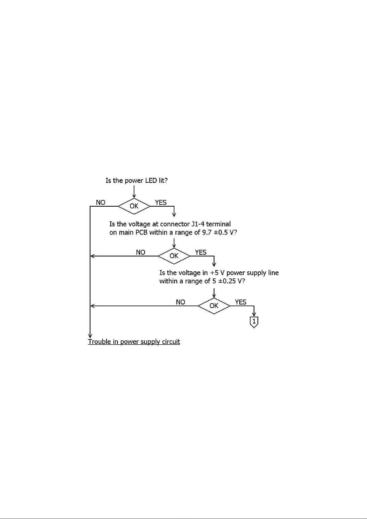
(A) No display
The built-in display of this System appea s in about ten seconds afte the powe switch is tu ned
on. If no display appea s in mo e than 15 seconds, check if the b ightness cont ol on the back pa-
nel is tu ned to the da k side – in such a case etu n to the "light" side (tu ning clockwise).
If no display still appea s, check as follows:
13
Set the VOLUME slide VR leve to the highest position. Set the CW/RTTY selecto to RTTY side.
Afte thus setting, is the AFSK monito sound oscillated when SEND-AUTO-RECEIVE selecto is set
to SEND and does the oscillation stop sho tly afte the selecto is etu ned to RECEIVE position?
P obable causes a e t ouble of c ystal oscillato
o dividing ci cuit, failu e of Compute o
w ong setting of CRTC. In the fi st place, check
the c ystal oscillato and dividing ci cuit.
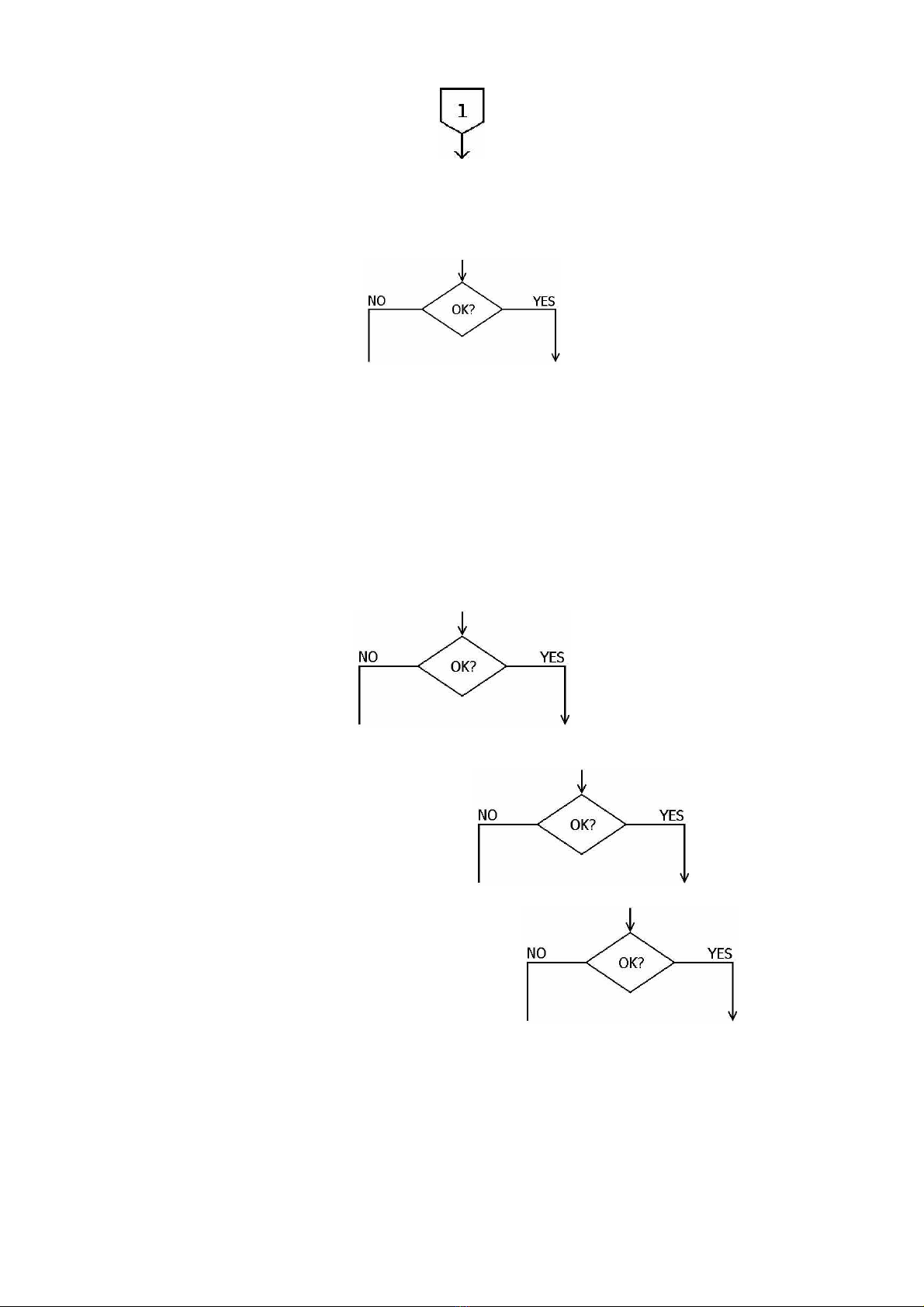
T ouble in CRTC block
Check the f equency of the following pa ts in the nume ical o de (checking of c ystal oscillato , di-
viding ci cuit):
1. Pin 6 of IC5 (13.5168 MHz)
2. Pin 9 of IC3 (6.7584 MHz)
3. Pin 5 of IC3 (3.3792 MHz)
4. Pin 39 of IC31 (3.3792 MHz)
Output has ceased to come out no mally;
t ouble of initially checked pa t.
Is the output of pin 37 of IC31 844.8 kHz?
IC31
is
b oken
Is
pin 40
of
IC31 at H
level?
R76 is b oken; C32 is sho ted; t ouble of RESET switch o
switch wi ing; b eakage of IC27, IC18, IC2, IC32, IC31
Compute is not wo king no mally

14
(B) Fluctuating display
The powe sou ce equi ements of this System a e voltage of DC 12 to 14.5 V and cu ent of not
less than 1.65 A.
Powe sou ce conditions
1. Stabilized powe sou ce is not necessa ily equi ed. The System can ope ate on a powe sou ce
containing slight ipples.
Howeve , the voltage should not be lowe than 12 V at the bottom of ipple. Below 12 V, the
pe fo mance of built-in display becomes unstable.
2. In the case of powe sou ce containing ipples, the ave age voltage should not be mo e than
14.5 V.
If the display sc een still fluctuates though confo ming to the equi ements above, check as fol-
lows:
Is the voltage at connecto te minal J1-4 on main PBC within a ange of 9.7 ±0.5 V?
ZD1 o IC48 is b oken Is the e any object emitting lines of magnetic
fo ce nea by (such as powe t ansfo me and
speake )?
W ong adjustment of V-HOLD o video cente of CRT unit,
o CRT unit is defective.
Remove the object.
15
(C) Abno mal exte nal display
Is built-in display no mal?
CRCT on COMPUTER BLOCK A e the VIDEO OUT te minal and exte nal dis-
play unit connected with 75-ohm coaxial cable
co ectly
without
any
sho ting
o
b eaking?
Connect
co ectly.
Is the exte nal
display a
home TV
set?
┌───────────────────────┘
The VIDEO OUT te minal of this system deli-
ve s a composite video signal of 1.0 ±0.2 Vpp
at 75 ohm load. The sync signal level is 30 %
and video signal level 70 %.
H-SYNC: 15.644 kHz; pulse width 5.32 µs
V-SYNC: 59.26 Hz; pulse width 2.1 ms
Non-inte laced aste scan system
Numbe of aste s: 264
Ho izontal display time: 42.61 µs
Ve tical display time: 14.06 ms
If the display unit does not confo m to the
conditions above, no mal ope ation is not ex-
pected. Usually, howeve , the V-SYNC and H-
HIGH may be adjusted at the monito TV set
side.
Home TV set cannot be connected to
VIDEO OUT te minal. Use video monito
TV set.
16
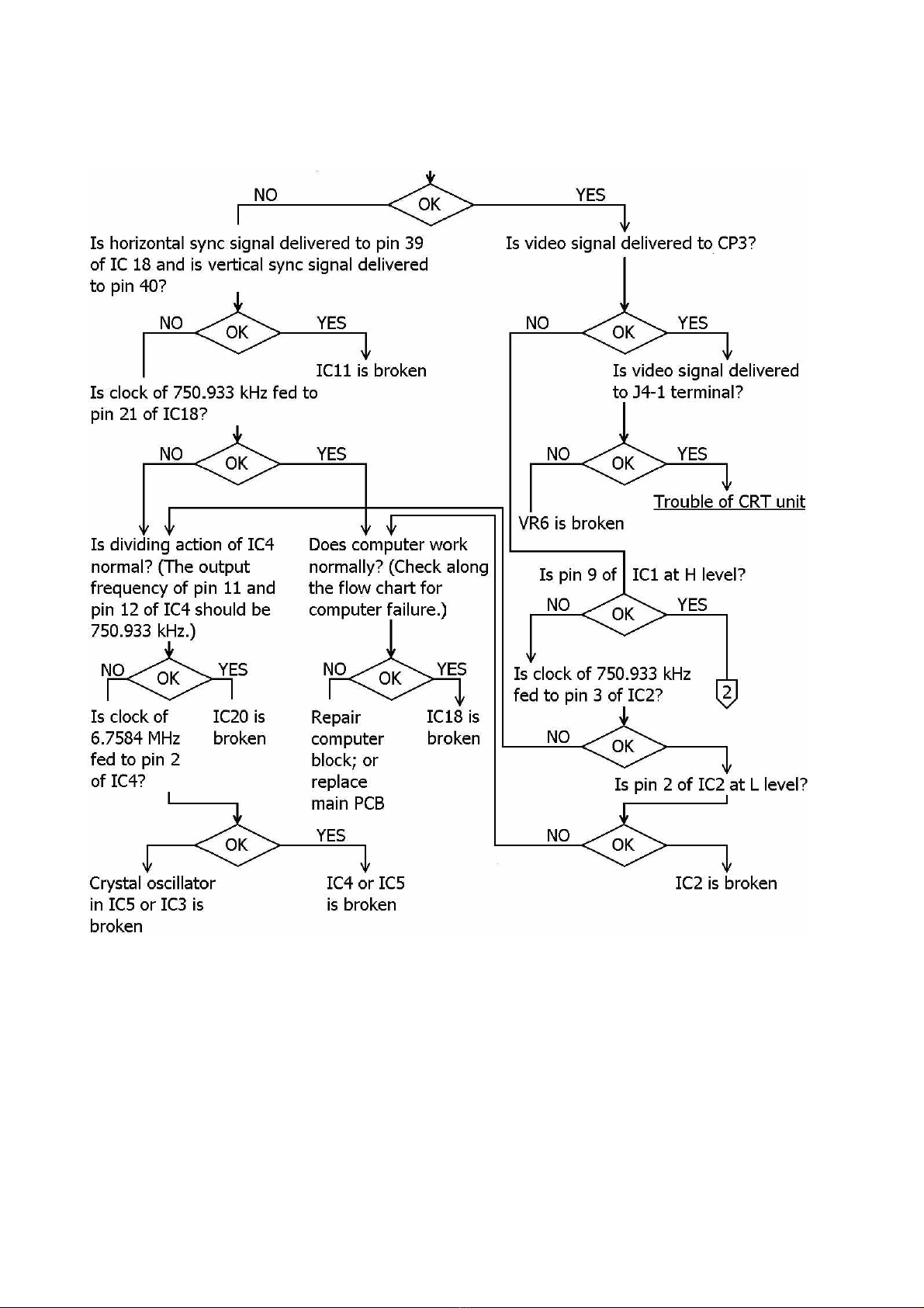
4.2 Tro ble of the CRTC block
Is ho izontal sync signal of about 63.92 µs pe iod delive ed to CP1, and is ve tical sync signal of
about 16.875 ms pe iod to CP2?

17

18

19
4.3 Tro ble of Comp ter block
Check whethe the Compute block is ope ating no mally o not in the following p ocedu e.
o The output level of pins 2, 4, 5, 6, of IC37 should be always H level as fa as the Compute
is ope ating no mally. When a pulse wavefo m of L level is obse ved on oscilloscope sc een,
it means that the Compute is unning away. Runaway of Compute is almost always ac-
companied by abno mal oscillation of the monito sound.
o As fa as the system is ope ating no mally, the Compute eads the state of switches, and
va ies the level of each Output po t as follows.
a. When the RX/TAPE selecto is set to RX side (since the switch is tu ned off, pin 4 of
IC40 becomes H level), pin 24 of IC28 is set to L level.
b. With the RX/TAPE selecto at RX position, when the RESET button is p essed, pin 24
of IC28 is set at H level while the button is being dep essed, and it is immediately
set to L level when the button is eleased.
c. When the RX/RAPE selecto is set to TAPE side(since the switch is tu ned off, pin 4
of IC40 becomes L level), pin 24 o IC28 is set to H level.
d. With the RX/TAPE selecto at TAPE position, while the RESET button is being p ess-
ed down, pin 24 of IC28 is set at H level, and immediately afte the button is ele-
ased, the level is set to L fo about 20 ms, and is then set to H again.
e. With the CW/RTTY selecto at RTTY, when the SEND-AUTO-RECEIVE selecto is set
at SEND (the switch is tu ned on, and pin 14 of IC40 becomes L level}, and pin 15
of IC27 is set to H level, and AFSK monito sound is delive ed. At the same time, pin
6 of IC27 is also set to H level. At this time, when an alphabetical o nume ical key
is p essed on the keyboa d, a co esponding code is sent out immediately, and the
f equency of AFSK monito sound is also va ied in tune with the code. In this state,
when the selecto is set to AUTO o RECEIVE position (the switch is tu ned off, and
pin 14 of IC40 becomes H level), about one second late , both pin 6 and pin 15 of
IC27 a e set to L level, and the AFSK monito sound ceases.
f. With the CW/RTTY selecto set at CW and SEND-AUTO-RECEIVE selecto at SEND
position, when an alphabetical o nume ical key is p essed on the keyboa d, a co e-
sponding code is sent out immediately, and the monito sound at 800 Hz is inte mit-
tently delive ed in tune with the code, and the CW LED flicke s at the same time.
o Of the ICs on the main PCB, those having high f equency of t ouble occu ences (b eaka-
ges) a e the following:
IC19 (SN74LS245)
IC7, ICS, IC9 (SN74LS157)
IC42 (MC3301, LM3900)
IC31 (MC6802, HD46802)
IC29 (2716 type E-PROM ... ope ation p og am w itten in)
IC30 (2732 type E-PROM ... ope ation p og am w itten in)
IC17 (2716 type E-PROM ... cha acte patte n w itten in)
IC6 (TC4011)

20
4.4 Tro ble in CW transmission
CW t ansmission is synch onized with CW sending clock.
The CW sending clock is made in IC35, and is fed f om CW sending clock input po t (pin 2 of IC40)
into the Compute block.
When this clock stops oscillation, CW cannot be t ansmitted.
The oscillation wavefo m at TP-3 is fixed at L level within about 15 to 20 µs, while the du ation of
H level va ies with the position of SPEED slide VR.
Since the monito sound, CW LED flicke ing, t ansceive t ansmission/ eception selection, and CW
key ope ation a e cont olled by the output of IC27, when the CW sending clock is no mal and
othe functional pa t is in t ouble, see the actions of exte nal cont ol signal output po ts (pa . 3.2).
4.5 Tro ble in CW reception
When eception of CW is in t ouble, check if signal appea s at check points of TP-5, TP-2, TP-4.
While efe ing to the flow of signal (pa . 2.2), check fo abno mal action. The TP-5 wavefo m
should be no mally satu ated (see below). About 10 % po tion is cut as shown below.
If malfunction often occu s due to noise, va y the esistance of R28. When the esistance is inc e-
ased, malfunction by noise dec eases, whe eas the sensitivity d ops.
It is also possible to dec ease malfunction by noise by adding 0.1 µF to C22 to make a total of
0.3 µF. In this case, howeve , high speed signals cannot be decoded. Simila ly, esistance to noise
is inc eased when C14 is changed to 22 µF, but the esponse speed of AGC is slowed down, so
that the esistance to QSB is weakened.
Table of contents
Other TELEREADER Media Converter manuals


