Plexim PLECS RT Box User manual

SPI interface loop-back demo on a single RT Box
1 Overview
The Serial Peripheral Interface (SPI) is a synchronous serial communication interface specification
used for short-distance communication, primarily with peripheral devices. SPI devices communicate
in full duplex mode using a master-slave architecture between a single master and multiple slaves.
The SPI Master block from the RT Box Target Support Library implements SPI communication via
digital outputs/inputs. There are 2 SPI modules available on the RT Box. Each SPI module can output
data on up to 4 paralleled data channels (using a common clock and chip select signal).
This demo model shows:
• a simple loop-back scenario that wires the SPI module digital output channel with the digital input
channel,
• how to configure the parameters inside the SPI Master block,
• SPI transmission within a single or multiple RT Box model steps.
One additional model shows the use case of the RT Box as SPI Master connected to an external ADC
device as the SPI slave. This additional model is explained in Appendix, and can be accessed by open-
ing the demo model folder.
1.1 Requirements
• One PLECS RT Box and one PLECS Coder license.
• The RT Box Target Support Package (minimum version 2.1.1).
• Follow the step-by-step instructions on configuring PLECS and the RT Box in the Quick Start guide
of the RT Box User Manual.
• One wire to connect the digital output channel 2 and digital input channel 2 on the front panel of
the RT Box.
2 Model
This demo model uses the SPI Master data output and data input on the same SPI module inside the
same subsystem. With the wiring between the SPI Master data output and input channel, a loop-back
of the SPI data is formed.
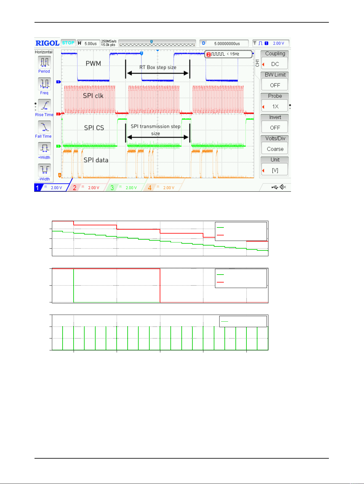
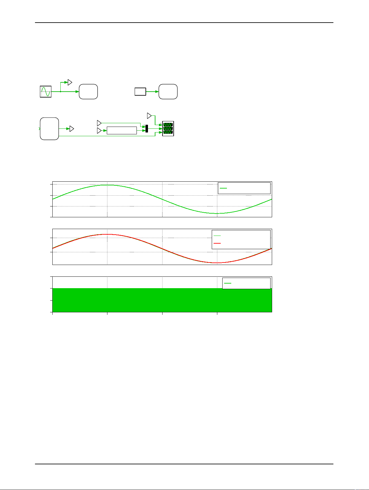
The circuit schematic is shown in Fig. 1. A Sine wave and a Pulse wave are packed into two 16-bit
words and transmitted out from the SPI Master data output channel. Through the loop-back wire, it
is received at the SPI Master data input channel, and then displayed in the Scope in Fig. 1 for com-
parison.
SPIMaster
v
SPI
Master
SineWave
Pulse
Generator
TX/RX
Overview
PWMOut
PWM
Out
0.5
TX
RX
TX
RX
Sine
Pulse
Figure 1: Subsystem circuit schematic for SPI loop-back demo
Additionally, a PWM Out block generates a PWM signal with 0.5 duty cycle synchronized with the RT
Box model step size by configuring its Synchronization with model step option as Enabled. This
PWM signal can be used as a reference to observe the different behaviors of SPI transmission within a
single or multiple RT Box model steps.
Fig. 2 shows the mask content of the SPI Master block. For the fields not mentioned in the following
explanation, please refer to the Help page of the SPI Master block.
www.plexim.com 1

SPI interface loop-back demo on a single RT Box
SPI Master Setup tab
Figure 2: Mask content of the SPI Master block
•SPI module: there are 2 SPI modules integrated into the RT Box for choosing, either SPI1 or SPI2.
• The Delay first clock after CS active and Hold CS active after last clock pulse fields are used
in case of special timing needed between the clock signal and CS (chip select) signal. In this demo
the default value of 1 (tick) is used in each field.
• The Delay CS after simulation step is useful to adjust the beginning of SPI data transmission
with regards to the RT Box simulation step. In this demo, Minimum is used by default.
•Mode [CPOL, CPHA]: Note that the same SPI mode has to be configured between the SPI Master
and an external SPI Slave device to ensure correct data interpretation.
•Skew-matched clock input can be enabled when the signal transmission delay from the master
output to its input exceeds half an SPI clock period. When enabled, the corresponding Digital in-
put channel for skew-matched SPI clock under Input tab has to be specified to receive the in-
coming clock, otherwise this field is greyed out.
•Number of parallel data channels: Note that the dimension of the Digital input channel(s)
for SPI data and Digital output channel(s) for SPI data under Input and Output tabs has to
match the number chosen here. In this demo only 1 data channel is used.
•Words per transmission: In this demo, one word is used for the Sine wave and the other word is
used for the Pulse wave.
•Sample time: Putting 0here means that the SPI transmission happens within every single model
www.plexim.com 2

SPI interface loop-back demo on a single RT Box
step. The SPI transmission can also be extended over multiple model steps by putting a number
here which is an integer multiple of the model step size. In the following section, it showcases both
scenarios. Besides, putting -1 means to inherit the sample time of the Atomic Subsystem or Task
frame that this SPI Master block resides in.
SPI Master Input and Output Tabs
Since each SPI module can only output one SPI clock signal and one CS signal, the Digital output
channel for SPI clock and Digital output channel for CS require both a single channel number.
3 Simulation
From the System tab of the Coder options... window, select the “Subsystem” and go to the Target
tab. Build the “RT Box” model onto the RT Box. Once the model is uploaded, from the External
Mode tab of the Coder options... window, Connect to the RT Box and Activate autotriggering.
The real-time simulation results can be observed via PLECS Scope called “TX/RX Overview”.
3.1 SPI Transmission within a Single Model Step
This is the default setup in the Model initialization commands of this demo model. It is done by en-
abling type = ‘single’, which sets:
• RT Box discretization step size = 20 µs
• SPI transmission sample time = 20 µs
Sinewave
Pulsewave
Validport
0
0
Time(s)
0.0 0.1 0.2 0.3 0.4
0.0
0.5
1.0
1.5
Reference
Receivedvalue
Reference
Receivedvalue
SPIMaster:v
Figure 3: Real-time simulation result on PLECS Scope for SPI transmission within a single model step
Once the real-time simulation is running on the RT Box and the external mode is enabled, the wave-
forms on “TX/RX Overview” Scope are shown in Fig. 3. The received value matches the reference value
in terms of amplitude and frequency for both the sine wave and the pulse wave, which validates the
SPI loop-back function.
www.plexim.com 3

SPI interface loop-back demo on a single RT Box
Fig. 4 shows the zoom-in of Fig. 3 around 0.3 s. The incoming SPI Master data exhibits a staircase
waveform with step size of 20 µs, which equals to the RT Box discretization step size. There is a delay
of two SPI transmission intervals between the outgoing reference signal and the received data.
Sinewave
Pulsewave
Validport
×1e4
3.20
3.25
3.30
0.0
0.5
1.0
×1e-1
Time(s)
2.9996 2.9998 3.0000 3.0002 3.0004
0.0
0.5
1.0
1.5
Reference
Receivedvalue
Reference
Receivedvalue
SPIMaster:v
Figure 4: Zoom-in around 0.3 s of the real-time simulation result on PLECS Scope for SPI transmission
within a single model step
For more insight on the timing, an external oscilloscope is used to measure the different digital chan-
nels and the RT Box step size. In Fig. 5 probe CH1 shows the 0.5 duty cycle PWM synchronized to the
20 µs model step size. Since the PWM is generated with positive polarity, from the center of the high
state to the center of the next high state marks exactly one model step. One can see that in this sce-
nario, the SPI transmission happens within every RT Box model step.
3.2 SPI Transmission over Multiple Model Steps
This scenario can be chosen by commenting out the previous type = ‘single’ and enabling
type = ‘multi’ in the model initialization commands of this demo model. This sets:
• RT Box discretization step size = 5 µs
• SPI transmission sample time = 20 µs
This is to demonstrate the case when the SPI transmission time (approx. SPI clock period x Bits per
word x Words per transmission) requires more time than what a single RT Box step offers. Note that
the SPI transmission interval can only be integer multiples of the RT Box step size.
The real-time simulation waveforms on the “TX/RX Overview” Scope look similar to Fig. 3 on a large
time scale. However, the zoom-in shown in Fig. 6 reveals the difference. For example, the Sine wave
reference signal is discretized with 5 µs now, while the incoming SPI data is still updated every 20 µs.
The complete SPI transmission takes 4 full RT Box calculation steps. There are still two SPI transmis-
sion steps delay in the loop-back scenario between the reference signal and the received data.
Fig. 7 provides more insight with the oscilloscope measurement. Probe CH1 shows the 0.5 duty cycle
PWM indicating the new 5 µs model step size. CH2 to CH4 show the SPI transmission at 20 µs sample
time, which are exactly 4 times a model step.
www.plexim.com 4

SPI interface loop-back demo on a single RT Box
Figure 5: External oscilloscope measurement for SPI transmission within a single model step
Sinewave
Pulsewave
Validport
×1e4
3.20
3.25
3.30
0.0
0.5
1.0
×1e-1
Time(s)
2.9996 2.9998 3.0000 3.0002 3.0004
0.0
0.5
1.0
1.5
Reference
Receivedvalue
Reference
Receivedvalue
SPIMaster:v
Figure 6: Zoom-in around 0.3 s of the real-time simulation result on PLECS Scope for SPI transmission
over multiple model steps
4 Conclusion
This RT Box demo model demonstrates a loop-back test using the integrated SPI interface on the RT
Box. It shows how to set up the SPI Master block in a PLECS model. The demo model runs in both
offline and in real-time simulation.
www.plexim.com 5

SPI interface loop-back demo on a single RT Box
Figure 7: External oscilloscope measurement for SPI transmission over multiple model steps
5 Appendix
For the SPI transmission with in a single model step size case, a more advanced demo is provided
with the name spi_demo_adc under the demo model folder. Fig. 8 depicts the setup and pin connection
for this scenario.
RT Box
AO-0
AGND
DI-1 (SPI RX)
DO-0 (SPI CLK)
DO-3 (SPI CS)
EVAL-AD7980-PMDZ (16-bit ADC)
Vin+
Vin- SDO
SCK
CNV
SDI
+Vcc
Figure 8: Pin connection between the RT Box and the external ADC board for the advanced SPI demo
The RT Box works as the SPI Master and generates a sinusoidal analog signal between 0.5 V and
4.5 V at 50 Hz. The 16-bit ADC evaluation board (EVAL-AD7980-PMDZ) converts this analog signal
into digital values and works as the SPI Slave to send the converted data to the RT Box SPI interface.
Note that in this demo the RT Box SPI CS signal is used as the CNV (conversion start) signal of the
ADC and the ADC SDI pin is tied up to the supply voltage. Please see section “3-WIRE CS MODE
WITHOUT BUSY INDICATOR” in [1]. In case of using two AD7980 devices together, one might need
specific timing patterns of CNV, and CS1 CS2 for SDI pin of each ADC. In this case, duty cycle and
carrier phase shift of the PWMs synchronized with the SPI transmission sample time can be properly
adjusted to achieve the desired signals.
The RT Box subsystem circuit schematic is shown in Fig. 9. Scope “Ref/RX Overview” shows the com-
www.plexim.com 6

SPI interface loop-back demo on a single RT Box
parison between the analog reference signal sent out from the RT Box and received SPI data after ex-
ternal ADC conversion.
Once the model is uploaded onto the RT Box and the external mode is enabled, the real-time simula-
tion results can be observed as shown in Fig. 10.
SPIMaster
v
SPI
Master
Ref/RX
Overview
PWMOut
PWM
Out
0.5
AnalogOut
Analog
Out
u/(2^16)*5
SineWave
RX
RX
RX
Ref
Ref
Figure 9: Subsystem circuit schematic for the advanced SPI demo on the RT Box
ExternalADCsampleddigitaldata(16-bit)
Digitaldataconvertedtoanalogvalue
Validport
×1e4
0
2
4
6
Voltage(V)
2
4
×1e-2
Time(s)
0.0 0.5 1.0 1.5
0.0
0.5
1.0
1.5
Receivedvalue
Analogreference
Receivedvalue
SPIMaster:v
Figure 10: Real-time simulation result on PLECS Scope of the advanced SPI demo
References
[1] Analog Devices AD7980 datasheet [Online]. Available: https://www.analog.com/media/en/technical-
documentation/data-sheets/AD7980.pdf.
www.plexim.com 7

Revision History:
RT Box Target Support Package 2.1.1 First release
How to Contact Plexim:
+41 44 533 51 00 Phone%
+41 44 533 51 01 Fax
Plexim GmbH Mail)
Technoparkstrasse 1
8005 Zurich
Switzerland
http://www.plexim.com Web
RT Box Demo Model
© 2002–2021 by Plexim GmbH
The software PLECS described in this document is furnished under a license agreement. The software
may be used or copied only under the terms of the license agreement. No part of this manual may be
photocopied or reproduced in any form without prior written consent from Plexim GmbH.
PLECS is a registered trademark of Plexim GmbH. MATLAB, Simulink and Simulink Coder are regis-
tered trademarks of The MathWorks, Inc. Other product or brand names are trademarks or registered
trademarks of their respective holders.
Other manuals for PLECS RT Box
7
This manual suits for next models
3
Table of contents
Other Plexim Media Converter manuals

Plexim
Plexim PLECS RT Box User manual

Plexim
Plexim PLECS RT Box User manual

Plexim
Plexim PLECS RT Box User manual

Plexim
Plexim PLECS RT Box User manual

Plexim
Plexim PLECS RT Box User manual

Plexim
Plexim PLECS RT Box User manual

Plexim
Plexim RT Box TSP 2.0.5 User manual

Plexim
Plexim PLECS RT Box User manual
Popular Media Converter manuals by other brands

ZyXEL Communications
ZyXEL Communications Ethernet-to-Fiber Media Converter... datasheet

Pinacl
Pinacl 2233 user manual

SMARTIX
SMARTIX DH16 quick start guide

Samson
Samson 611 Mounting and operating instructions

Midimuso
Midimuso CV-12 Assembly instructions

Menards
Menards MASTERFORCE 260-9519 Operator's manual