2.1.6 J6 – GND Bottom Converter
2.1.7 J7 – ENABLE Bottom Converter
2.1.8 J8 – TRACK Bottom Converter
2.1.9 J9 – CLK Bottom Converter
2.1.10 J10 – VOUT Bottom Converter
2.1.11 J11 – GND
2.1.12 J12 – PG Top Converter
2.1.13 J13 – PG Bottom Converter
3 Performance Specifications
3.1 Top Converter Specification
www.ti.com
Performance Specifications
This is the return connection for the input power supply of the bottom converter.
Pin 1 of this connector is tied to the EN pin of the bottom converter. Pin 2 of this connector is tied to theground plane of the bottom converter. Shorting pin 1 to 2 will disable the converter. Leaving pin 1 and 2open enables the bottom converter.
Pin 1 of this connector is tied to the SS pin of the bottom converter. Pin 2 of this connector is tied to theground plane of the bottom converter. Shorting pin 1 to 2 will disable the converter. Leaving pin 1 and 2open enables the bottom converter.
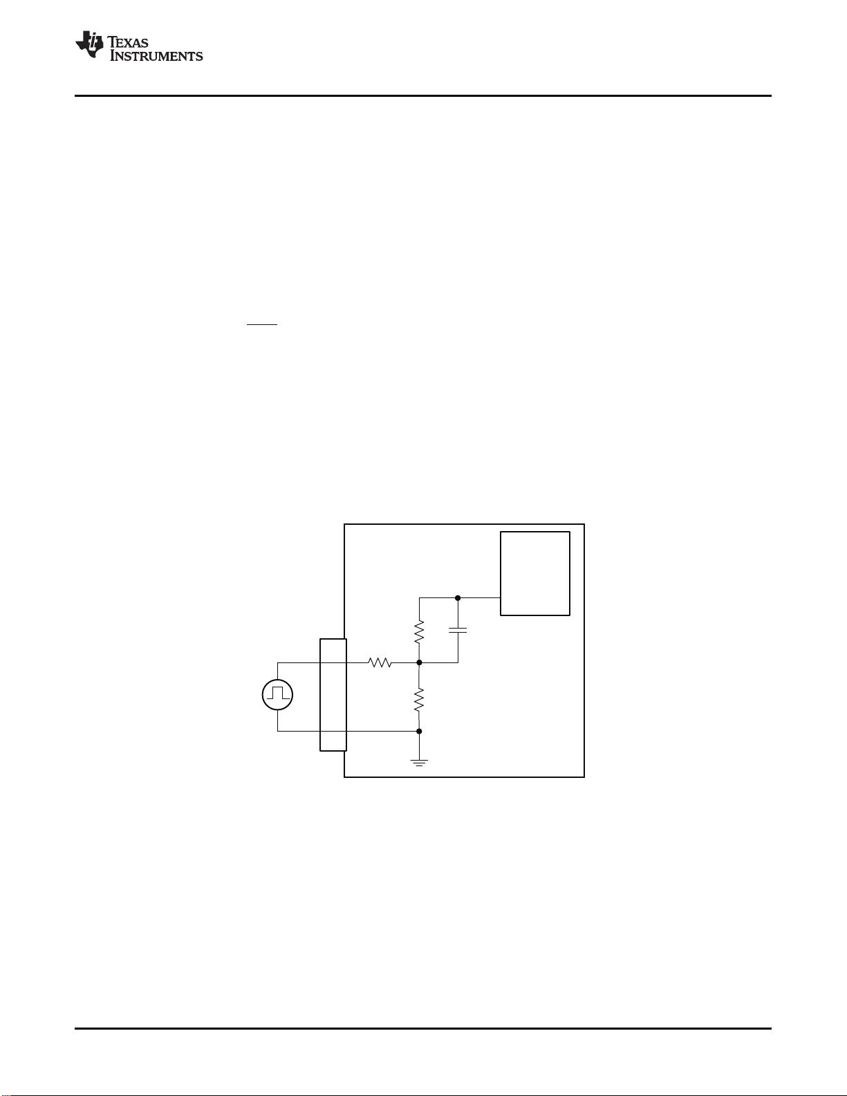
Pin 1 of this connector is tied to the RT/CLK pin of the bottom converter. Pin 2 of this connector is tied tothe ground plane of the bottom converter.
This is the positive connection from the output of the bottom converter. Connect this pin to the positiveinput of the load.
This is the return connection for the output of the bottom converter.
Pin 1 of this connector is tied to the PWRGD output pin of the top converter. Pin 2 of this connector is tiedto the ground plane of the top converter. R4 is pull up resistor for the PG pin and is connected to theoutput voltage. The maximum voltage of the PWRGD pin is 6V. If the output voltage of the converter is setto any value higher than 6.0V, then R4 must be removed from the board to avoid damaging theTPS54160.
Pin 1 of this connector is tied to the PWRGD pin of the bottom converter. Pin 2 of this connector is tied tothe ground plane of the bottom converter. R12 is pull up resistor for the PG pin and is connected to theoutput voltage. The maximum voltage of the PWRGD pin is 6V. If the output voltage of the converter is setto any value higher than 6.0V, then R12 must be removed from the board to avoid damaging theTPS54160.
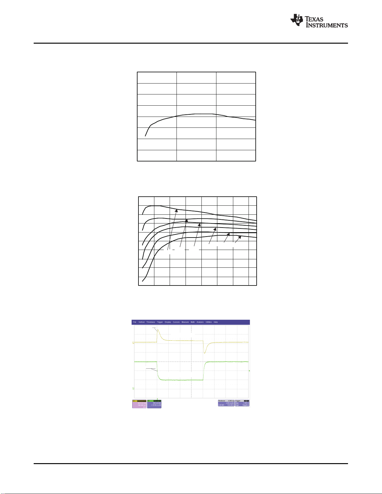
Table 1 provides a summary of the top converters specifications. The top converter is designed and testedfor VIN = 31.5V to 52.5V. Operation at other input voltages is possible but some performancespecifications will vary compared to those shown in Table 2 . The ambient temperature is 25 °C for allmeasurements, unless otherwise noted.
SLVU270 – September 2008 TPS54160EVM-230 3Submit Documentation Feedback