Thales Cinterion PLS63-W Installation guide
Cinterion®PLS63-W
Hardware Interface Overview
Version: 00.860
DocId: PLS63-W_HIO_v00.860

GENERAL NOTE
THE USE OF THE PRODUCT INCLUDING THE SOFTWARE AND DOCUMENTATION (THE "PROD-
UCT") IS SUBJECT TO THE RELEASE NOTE PROVIDED TOGETHER WITH PRODUCT. IN ANY
EVENT THE PROVISIONS OF THE RELEASE NOTE SHALL PREVAIL. THIS DOCUMENT CONTAINS
INFORMATION ON THALES DIS AIS DEUTSCHLAND GMBH (“THALES”) PRODUCTS. THE SPECIFI-
CATIONS IN THIS DOCUMENT ARE SUBJECT TO CHANGE AT THALES'S DISCRETION. THALES
GRANTS A NON-EXCLUSIVE RIGHT TO USE THE PRODUCT. THE RECIPIENT SHALL NOT TRANS-
FER, COPY, MODIFY, TRANSLATE, REVERSE ENGINEER, CREATE DERIVATIVE WORKS; DISAS-
SEMBLE OR DECOMPILE THE PRODUCT OR OTHERWISE USE THE PRODUCT EXCEPT AS
SPECIFICALLY AUTHORIZED. THE PRODUCT AND THIS DOCUMENT ARE PROVIDED ON AN "AS
IS" BASIS ONLY AND MAY CONTAIN DEFICIENCIES OR INADEQUACIES. TO THE MAXIMUM
EXTENT PERMITTED BY APPLICABLE LAW, THALES DISCLAIMS ALL WARRANTIES AND LIABILI-
TIES. THE RECIPIENT UNDERTAKES FOR AN UNLIMITED PERIOD OF TIME TO OBSERVE
SECRECY REGARDING ANY INFORMATION AND DATA PROVIDED TO HIM IN THE CONTEXT OF
THE DELIVERY OF THE PRODUCT. THIS GENERAL NOTE SHALL BE GOVERNED AND CON-
STRUED ACCORDING TO GERMAN LAW.
Copyright
Transmittal, reproduction, dissemination and/or editing of this document as well as utilization of its con-
tents and communication thereof to others without express authorization are prohibited. Offenders will be
held liable for payment of damages. All rights created by patent grant or registration of a utility model or
design patent are reserved.
Copyright © 2021, THALES DIS AIS Deutschland GmbH
Trademark Notice
Thales, the Thales logo, are trademarks and service marks of Thales and are registered in certain coun-
tries. Microsoft and Windows are either registered trademarks or trademarks of Microsoft Corporation in
the United States and/or other countries. All other registered trademarks or trademarks mentioned in this
document are property of their respective owners.
tPLS63-W_HIO_v00.860 2021-02-18
Confidential / Preliminary
Cinterion®PLS63-W Hardware Interface Overview
2
Page 2 of 61
Document Name: Cinterion®PLS63-W Hardware Interface Overview
Version: 00.860
Date: 2021-02-18
DocId: PLS63-W_HIO_v00.860
Status Confidential / Preliminary

Cinterion®PLS63-W Hardware Interface Overview
Contents
61
tPLS63-W_HIO_v00.860 2021-02-18
Confidential / Preliminary
Page 3 of 61
Contents
1 Introduction ................................................................................................................. 7
1.1 Product Variants ................................................................................................ 7
1.2 Key Features at a Glance .................................................................................. 7
1.3 PLS63-W System Overview............................................................................. 11
2 Interface Characteristics .......................................................................................... 12
2.1 Application Interface ........................................................................................ 12
2.1.1 USB Interface...................................................................................... 12
2.1.2 Serial Interface ASC0 ......................................................................... 13
2.1.3 Serial Interface ASC1 ......................................................................... 14
2.1.4 UICC/SIM/USIM Interface................................................................... 15
2.1.4.1 SIM_SWITCH Line.............................................................. 17
2.1.5 GPIO Interface .................................................................................... 18
2.1.6 Digital Audio Interface......................................................................... 18
2.1.6.1 Pulse Code Modulation Interface ........................................ 18
2.1.6.2 Inter-IC Sound Interface (TBD) ........................................... 19
2.1.7 Control Signals.................................................................................... 20
2.1.7.1 Status LED .......................................................................... 20
2.1.7.2 Power Indication.................................................................. 21
2.2 RF Antenna Interface....................................................................................... 22
2.2.1 Antenna Installation ............................................................................ 23
2.2.2 RF Line Routing Design...................................................................... 24
2.2.2.1 Line Arrangement Examples ............................................... 24
2.2.2.2 Routing Example ................................................................. 29
2.3 GNSS Antenna Interface ................................................................................. 30
2.3.1 GNSS Antenna Diagnostic.................................................................. 31
3 Operating Characteristics ........................................................................................ 32
3.1 Power Supply................................................................................................... 32
4 Mechanical Dimensions, Mounting and Packaging............................................... 33
4.1 Mechanical Dimensions of PLS63-W............................................................... 33
5 Regulatory and Type Approval Information ........................................................... 37
5.1 Directives and Standards................................................................................. 37
5.2 SAR requirements specific to portable mobiles ............................................... 40
5.3 Reference Equipment for Type Approval......................................................... 41
5.4 Compliance with FCC/IC/ISED Rules and Regulations ................................... 42
6 Document Information.............................................................................................. 45
6.1 Revision History ............................................................................................... 45
6.2 Related Documents ......................................................................................... 45
6.3 Terms and Abbreviations ................................................................................. 45
6.4 Safety Precaution Notes .................................................................................. 49

Cinterion®PLS63-W Hardware Interface Overview
Contents
61
tPLS63-W_HIO_v00.860 2021-02-18
Confidential / Preliminary
Page 4 of 61
7 Appendix.................................................................................................................... 50
7.1 List of Parts and Accessories........................................................................... 50

Cinterion®PLS63-W Hardware Interface Overview
Tables
tPLS63-W_HIO_v00.860 2021-02-18
Confidential / Preliminary
Page 5 of 61
Tables
Table 1: Signals of the SIM interface (SMT application interface) ............................... 15
Table 2: GPIO lines and possible alternative assignment............................................ 18
Table 3: Overview of PCM pin functions...................................................................... 19
Table 4: Overview of I2S pin functions ......................................................................... 20
Table 5: Return loss in the active band........................................................................ 22
Table 6: Sample ranges of the GNSS antenna diagnostic measurements and their
possible meaning ........................................................................................... 31
Table 7: Directives ....................................................................................................... 37
Table 8: Standards of North American type approval .................................................. 37
Table 9: Standards of European type approval............................................................ 37
Table 10: Requirements of quality ................................................................................. 38
Table 11: Standards of the Ministry of Information Industry of the
People’s Republic of China............................................................................ 38
Table 12: Toxic or hazardous substances or elements with defined concentration
limits............................................................................................................... 39
Table 13: Antenna gain limits for FCC and ISED........................................................... 42
Table 14: List of parts and accessories.......................................................................... 50
Table 15: Molex sales contacts (subject to change) ...................................................... 51

Cinterion®PLS63-W Hardware Interface Overview
Figures
tPLS63-W_HIO_v00.860 2021-02-18
Confidential / Preliminary
Page 6 of 61
Figures
Figure 1: PLS63-W system overview ............................................................................ 11
Figure 2: USB circuit ..................................................................................................... 12
Figure 3: Serial interface ASC0..................................................................................... 13
Figure 4: Serial interface ASC1..................................................................................... 14
Figure 5: Module’s two UICC/SIM/USIM interfaces ...................................................... 16
Figure 6: UICC/SIM/USIM interfaces connected........................................................... 16
Figure 7: External UICC/SIM/USIM switch.................................................................... 17
Figure 8: Sample circuit for SIM interface connection via SIM switch........................... 17
Figure 9: Status signaling with LED driver .................................................................... 20
Figure 10: Power indication signal .................................................................................. 21
Figure 11: Antenna pads (bottom view) .......................................................................... 23
Figure 12: Embedded Stripline with 65µm prepreg (1080) and 710µm core .................. 24
Figure 13: Micro-Stripline on 1.0mm standard FR4 2-layer PCB - example 1 ................ 25
Figure 14: Micro-Stripline on 1.0mm Standard FR4 PCB - example 2............................ 26
Figure 15: Micro-Stripline on 1.5mm Standard FR4 PCB - example 1............................ 27
Figure 16: Micro-Stripline on 1.5mm Standard FR4 PCB - example 2............................ 28
Figure 17: Routing to application‘s RF connector ........................................................... 29
Figure 18: PLS63-W evaluation board layer table........................................................... 29
Figure 19: Supply voltage for active GNSS antenna....................................................... 30
Figure 20: ESD protection for passive GNSS antenna ................................................... 31
Figure 21: Decoupling capacitor(s) for BATT+................................................................ 32
Figure 22: PLS63-W– top and bottom viewDimensions of
PLS63-W (all dimensions in mm)................................................................... 34
Figure 23: Dimensions of PLS63-W (all dimensions in mm)........................................... 35
Figure 24: Dimensions of PLS63-W (keepout area recommended)................................ 36
Figure 25: Reference equipment for Type Approval ....................................................... 41

Cinterion®PLS63-W Hardware Interface Overview
1 Introduction
11
tPLS63-W_HIO_v00.860 2021-02-18
Confidential / Preliminary
Page 7 of 61
1 Introduction
This document1describes the hardware of the Cinterion®PLS63-W module. It helps you quick-
ly retrieve interface specifications, electrical and mechanical details and information on the re-
quirements to be considered for integrating further components.
1.1 Product Variants
This document applies to the following Thales module variants:
•Cinterion
®PLS63-W Module
1.2 Key Features at a Glance
1. The document is effective only if listed in the appropriate Release Notes as part of the technical docu-
mentation delivered with your Thales product.
Feature Implementation
General
Frequency bands PLS63-W integrates all the bands required to have a global coverage
across the world (NORAM / LATAM / EMEA /APAC).
GSM class Small MS
Output power (according
to release 99)
Class 4 (+33dBm ±2dB) for GSM850
Class 4 (+33dBm ±2dB) for GSM900
Class 1 (+30dBm ±2dB) for GSM1800
Class 1 (+30dBm ±2dB) for GSM1900
Class E2 (+27dBm ± 3dB) for GSM 850 8-PSK
Class E2 (+27dBm ± 3dB) for GSM 900 8-PSK
Class E2 (+26dBm +3 /-4dB) for GSM 1800 8-PSK
Class E2 (+26dBm +3 /-4dB) for GSM 1900 8-PSK
Output power (according
to Release 99)
Class 3 (+24dBm +1/-3dB) for UMTS 850, WCDMA FDD BdXIX
Class 3 (+24dBm +1/-3dB) for UMTS 850, WCDMA FDD BdVI
Class 3 (+24dBm +1/-3dB) for UMTS 850, WCDMA FDD BdV
Class 3 (+24dBm +1/-3dB) for UMTS 900, WCDMA FDD BdVIII
Class 3 (+24dBm +1/-3dB) for UMTS 1700, WCDMA FDD BdIII
Class 3 (+24dBm +1/-3dB) for UMTS 1900, WCDMA FDD BdII
Class 3 (+24dBm +1/-3dB) for UMTS 2100, WCDMA FDD BdIV
Class 3 (+24dBm +1/-3dB) for UMTS 2100, WCDMA FDD BdI
Cinterion®PLS63-W Hardware Interface Overview
1.2 Key Features at a Glance
11
tPLS63-W_HIO_v00.860 2021-02-18
Confidential / Preliminary
Page 8 of 61
Output power (according
to Release 8)
Class 3 (+23dBm ±2dB) for LTE 600, LTE FDD Bd71
Class 3 (+23dBm ±2dB) for LTE 700, LTE FDD Bd12 <MFBI Bd17>
Class 3 (+23dBm ±2dB) for LTE 700, LTE FDD Bd13
Class 3 (+23dBm ±2dB) for LTE 700, LTE FDD Bd14
Class 3 (+23dBm+2/-2.5dB) for LTE 700, LTE FDD Bd28
Class 3 (+23dBm ±2dB) for LTE 850, LTE FDD Bd26
Class 3 (+23dBm ±2dB) for LTE 850, LTE FDD Bd18
Class 3 (+23dBm ±2dB) for LTE 850, LTE FDD Bd19
Class 3 (+23dBm ±2dB) for LTE 800, LTE FDD Bd20
Class 3 (+23dBm ±2dB) for LTE 850, LTE FDD Bd5
Class 3 (+23dBm ±2dB) for LTE 900, LTE FDD Bd8
Class 3 (+23dBm ±2dB) for LTE 1800, LTE FDD Bd3
Class 3 (+23dBm ±2dB) for LTE 1900, LTE FDD Bd2
Class 3 (+23dBm ±2dB) for LTE 1900, LTE FDD Bd25
Class 3 (+23dBm ±2dB) for LTE 2100, LTE FDD Bd1
Class 3 (+23dBm ±2dB) for LTE 2100, LTE FDD Bd4
Class 3 (+23dBm ±2dB) for LTE 2100, LTE FDD Bd66
Class 3 (+23dBm ±2dB) for LTE 2600, LTE FDD Bd7
Class 3 (+23dBm ±2dB) for LTE 2300, LTE TDD Bd40
Class 3 (+23dBm ±2dB) for LTE 2500, LTE TDD Bd41
Class 3 (+23dBm ±2dB) for LTE 2600, LTE TDD Bd38
Power supply Normal operation:
3.0V < VBATT+ < 4.5V
Typ value is 3.8V
Extended operation: TBD
Operating temperature
(board temperature)
Normal operation: -30°C to +85°C
Extended operation: -40°C to -30°C, +85°C to +90°C
Physical Dimensions: 33mm x 29mm x 2.31mm
Weight: approx. 4.8g
RoHS All hardware components fully compliant with EU RoHS Directive
LTE features
3GPP Release 10 UE CAT 1 for PLS63 (DL 10Mbps, UL 5Mbps)
HSPA feature
3GPP Release 7 UE CAT. 8, 6 for PLS63
HSDPA – DL 7.2Mbps
HSUPA – UL 5.7Mbps
Compressed mode (CM) supported according to 3GPP TS25.212
UMTS features
3GPP Release 4 PS data rate – 384 kbps DL / 384 kbps UL
CS data rate – 64 kbps DL / 64 kbps UL
Feature Implementation

Cinterion®PLS63-W Hardware Interface Overview
1.2 Key Features at a Glance
11
tPLS63-W_HIO_v00.860 2021-02-18
Confidential / Preliminary
Page 9 of 61
GSM/GPRS/EGPRS features
Data transfer GPRS:
• Multislot Class 12
• Mobile Station Class B
• Coding Scheme 1 – 4
EGPRS:
• Multislot Class 12
• EDGE E2 power class for 8 PSK
• Downlink coding schemes – CS 1-4, MCS 1-9
• Uplink coding schemes – CS 1-4, MCS 1-9
• SRB loopback and test mode B
• 8-bit, 11-bit RACH
• 1 phase/2 phase access procedures
• Link adaptation and IR
• NACC, extended UL TBF
• Mobile Station Class B
SMS Point-to-point MT and MO
Cell broadcast
Text and PDU mode
Storage: SIM card plus SMS locations in mobile equipment
GNSS Features
Protocol NMEA
Modes Standalone GNSS (GPS, GLONASS, Beidou, Galileo)
General Automatic power saving modes.
DC feed bridge and control of power supply for active antenna
Software
AT commands Hayes 3GPP TS 27.007, TS 27.005, Thales
SIM Application Toolkit Default (Network) bearer support for BIP
Firmware update Generic update from host application over USB modem
Interfaces
Module interface Surface mount device with solderable connection pads (SMT application
interface). Land grid array (LGA) technology ensures high solder joint reli-
ability and allows the use of an optional module mounting socket.
For more information on how to integrate SMT modules see also [4].This
application note comprises chapters on module mounting and application
layout issues as well as on additional SMT application development equip-
ment.
USB USB 2.0 High Speed (480Mbit/s) device interface. Full Speed (12Mbit/s)
compliant.
Feature Implementation
Cinterion®PLS63-W Hardware Interface Overview
1.2 Key Features at a Glance
11
tPLS63-W_HIO_v00.860 2021-02-18
Confidential / Preliminary
Page 10 of 61
2 serial interfaces ASC0 (in parts shared with GPIO lines):
• 8-wire modem interface with status and control lines, unbalanced, asyn-
chronous
• Fixed baud rates: 300bps to 921,600bps
• Supports RTS0/CTS0 hardware flow control.
ASC1 (shared with GPIO lines):
• 4-wire, unbalanced asynchronous interface
• Fixed baud rates: 300bps to 921,600bps and 3Mbps
• Supports RTS1/CTS1 hardware flow control
Audio 1 digital interface (PCM), shared with GPIO lines
2 UICC interfaces
(switchable)
Supported chip cards: UICC/SIM/USIM 3V, 1.8V
GPIO interface 22 GPIO lines comprising:
13 lines shared with ASC0, ASC1 lines, with network status indication, fast
shutdown and SIM switch
4 GPIO lines shared with PCM interface
9 GPIO lines not shared
I2C interface Supports I2C serial interface.
Digital audio interface 1 digital interface can be configured as PCM or I2S(TBD).
RING0 Support RING0 to wake up host from power down modes
Antenna interface pads 50Ω. UMTS/GSM/LTE main antenna, UMTS/LTE Rx Diversity antenna,
GNSS antenna.
ADC inputs Analog-to-Digital Converter with unbalanced analog inputs, for example, for
the (external) antenna diagnosis
Power on/off, Reset
Power on/off Switch on by hardware signal IGT
Switch off by AT command
Switch off by hardware signal FST_SHDN instead of AT command
Automatic switch off in case of critical temperature or voltage conditions
Reset Orderly reset by AT command
Reset by emergency reset signal EMERG_RST.
Special features
Real time clock Timer functions via AT commands.
Evaluation kit
LGA DevKit LGA DevKit designed to test Thales LGA modules.
Evaluation module PLS63-W module soldered onto a dedicated PCB that can be connected to
an adapter in order to be mounted onto the DSB75 or DSB mini.
DSB-mini DSB-mini Development Support Board designed to test and type approve.
It is the cost optimized development board alternative to DSB75.
DSB75 DSB75 Development Support Board designed to test and type approve
Thales modules and provide a sample configuration for application engi-
neering. A special adapter is required to connect the PLS63-W evaluation
module to the DSB75.
Feature Implementation
Cinterion®PLS63-W Hardware Interface Overview
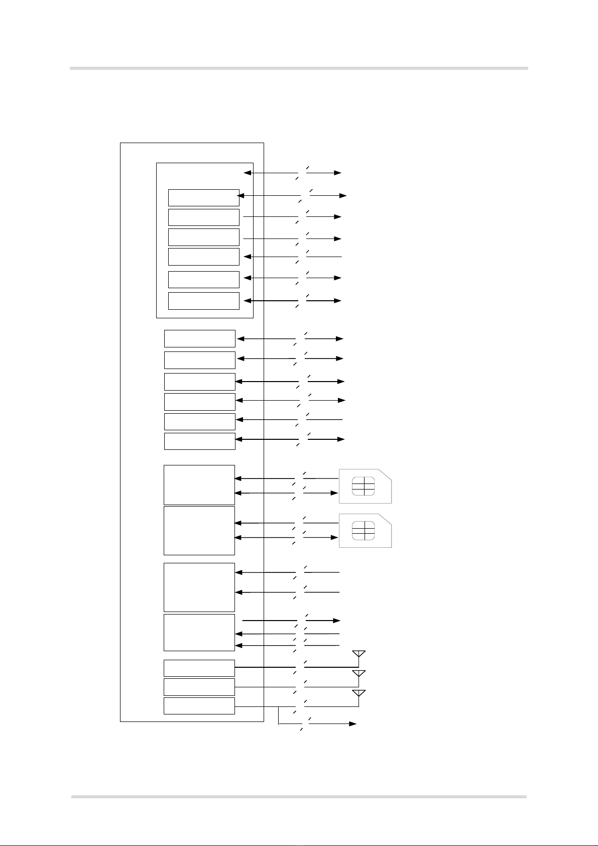
1.3 PLS63-W System Overview
11
tPLS63-W_HIO_v00.860 2021-02-18
Confidential / Preliminary
Page 11 of 61
1.3 PLS63-W System Overview
Figure 1: PLS63-W system overview
GPIO
ASC1/GPIO
STATUS
Digital Audio
SIM_SWITCH
FST_SHDN
ASC0/GPIO
PWR_IND
I2C
USB
ADC
SIM1 interface(with
SIM card detection)
SIM2 interface(with
SIM card detection)
CONTROL
Power Supply
RF_Main_Path
Diversity_RX
GNSS_Path
9
1
1
1
4
2
3
3
5
1SIM1 Card
5
1SIM2 Card
1
1
1
1
1
1
1
GPIO
Serial Interface/GPIO
STATUS/GPIO
PCM(I2S) Interface&MCLK
SIM_SWITCH/GPIO
Fast Shutdown/GPIO
Serial Interface/GPIO
I2C
USB
ADC
IGT
EMERG_RST
Base Band Power
RF Power
Main Antenna
Diversity Antenna
GNSS Antenna
Module
Application
Power Indicator
4
Digital Audio PCM/GPIO
1
ASC0/GPIO Serial Interface 0
4
3
2
VGNSS
1GNSS_DC
1

Cinterion®PLS63-W Hardware Interface Overview
2 Interface Characteristics
31
tPLS63-W_HIO_v00.860 2021-02-18
Confidential / Preliminary
Page 12 of 61
2 Interface Characteristics
PLS63-W is equipped with an SMT application interface that connects to the external applica-
tion. The SMT application interface incorporates the various application interfaces as well as
the RF antenna interface.
2.1 Application Interface
2.1.1 USB Interface
PLS63-W supports a USB 2.0 High Speed (480Mbit/s) device interface that is Full Speed
(12Mbit/s) compliant. The USB I/O pins are capable of driving the signal at min 3.0V. The im-
pedances, serial and pull up resistors are implemented according to “Universal Serial Bus
Specification Revision 2.0”1, No further additional components are required.
The external application is responsible for supplying the VUSB_IN line. This line is used for ca-
ble detection only. The USB part (driver and transceiver) is supplied by means of BATT+. This
is because PLS63-W is designed as a self-powered device compliant with the “Universal Serial
Bus Specification Revision 2.0”.
Figure 2: USB circuit
To properly connect the module's USB interface to the external application, a USB 2.0 compat-
ible connector and cable or hardware design is required. For more information on the USB re-
lated signals see Table 3. Furthermore, the USB modem driver distributed with PLS63-W
needs to be installed.
1. The specification is ready for download on http://www.usb.org/developers/docs/
VBUS
DP
DN
VREG (3V075)
BATT+
USB_DP2)
lin. reg.
GND
Module
Detection only VUSB_IN
USB part1)
1) All serial (including R
S) and pull-up resistors for data lines are implemented.
USB_DN2)
2) If the USB interface is operated in High Speed mode(480MHz), it is recommended to take
special care routing the data lines USB_DP and USB_DN. Application layout should in this
case implement a differential impedance of90 ohms for proper signal integrity.
RS
RS
SMT
Cinterion®PLS63-W Hardware Interface Overview
2.1 Application Interface
31
tPLS63-W_HIO_v00.860 2021-02-18
Confidential / Preliminary
Page 13 of 61
While a USB connection is active, the module will never switch to SLEEP mode. Only if the USB
interface is in Suspend mode, the module is able to switch to SLEEP mode.
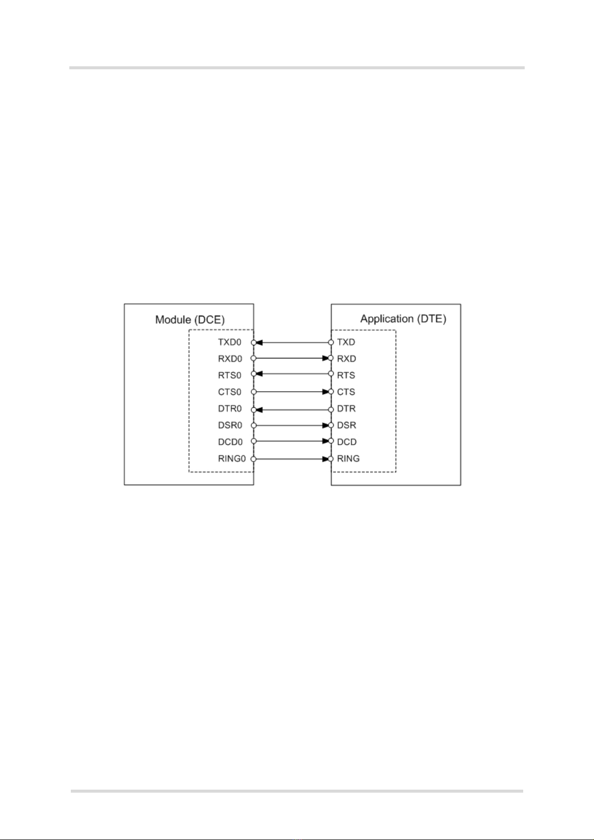
2.1.2 Serial Interface ASC0
PLS63-W offers an 8-wire unbalanced, asynchronous modem interface ASC0 conforming to
ITU-T V.24 protocol DCE signaling. The electrical characteristics do not comply with ITU-T
V.28. The significant levels are 0V (for low data bit or active state) and 1.8V (for high data bit
or inactive state). For electrical characteristics please refer to Table 3.
PLS63-W is designed for use as a DCE. Based on the conventions for DCE-DTE connections
it communicates with the customer application (DTE) using the following signals:
• Port TXD @ application sends data to the module’s TXD0 signal line
• Port RXD @ application receives data from the module’s RXD0 signal line
Figure 3: Serial interface ASC0
Features:
• Includes the data lines TXD0 and RXD0, the status lines RTS0 and CTS0 and, in addition,
the modem control lines DTR0, DSR0, DCD0 and RING0.
• The RING0 signal serves to indicate incoming calls and other types of URCs (Unsolicited
Result Code). It can also be used to send pulses to the host application, for example to
wake up the application from power saving state.
• Configured for 8 data bits, no parity and 1 stop bit.
• ASC0 can be operated at fixed bit rates from 300bps up to 921600bps.
• Supports RTS0/CTS0 hardware flow control. The hardware hand shake line RTS0 has an
internal pull down resistor causing a low level signal, if the line is not used and open.
Although hardware flow control is recommended, this allows communication by using only
RXD and TXD lines.
Note: The ASC0 modem control lines DTR0, DCD0, DSR0 and RING0 can also be configured
as GPIO lines. If configured as GPIO lines, these GPIO lines are assigned as follows:
GPIO1-->DTR0
GPIO2-->DCD0
GPIO3-->DSR0
GPIO24-->RING0
Cinterion®PLS63-W Hardware Interface Overview
2.1 Application Interface
31
tPLS63-W_HIO_v00.860 2021-02-18
Confidential / Preliminary
Page 14 of 61
Configuration is done by AT command (see [1]). The configuration is non-volatile and becomes
active after a module restart.
Notes: No data must be sent over the ASC0 interface before the interface is active and ready
to receive data (see Section 3.1.1).
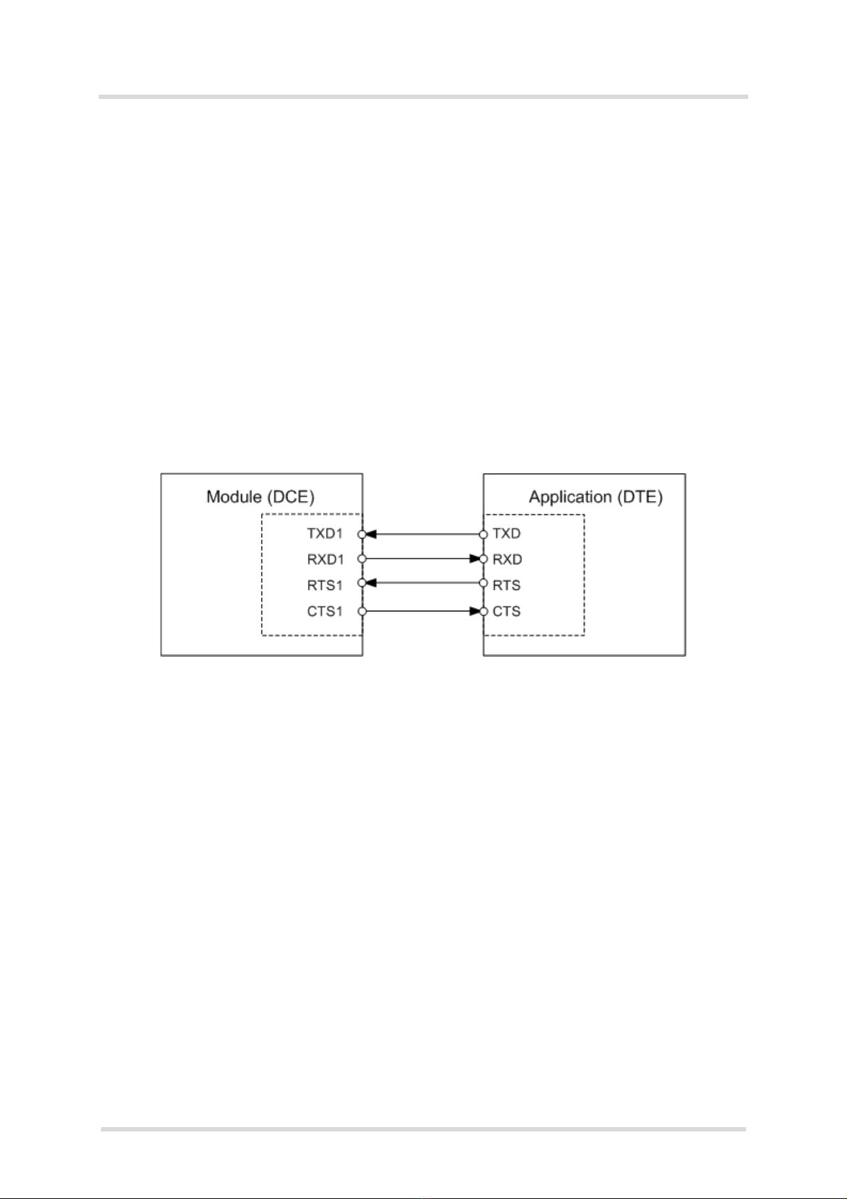
2.1.3 Serial Interface ASC1
Four PLS63-W GPIO lines can be configured as ASC1 interface signals to provide a 4-wire un-
balanced, asynchronous modem interface ASC1 conforming to ITU-T V.24 protocol DCE sig-
nalling. The electrical characteristics do not comply with ITU-T V.28. The significant levels are
0V (for low data bit or active state) and 1.8V (for high data bit or inactive state). For electrical
characteristics please refer to Table 3.
PLS63-W is designed for use as a DCE. Based on the conventions for DCE-DTE connections
it communicates with the customer application (DTE) using the following signals:
• Port TXD @ application sends data to module’s TXD1 signal line
• Port RXD @ application receives data from the module’s RXD1 signal line
Figure 4: Serial interface ASC1
Features
• Includes only the data lines TXD1 and RXD1 plus RTS1 and CTS1 for hardware hand-
shake.
• On ASC1 no RING line is available.
• Configured for 8 data bits, no parity and 1 or 2 stop bits.
• ASC1 can be operated at fixed bit rates from 300 bps to 921,600bps and 3Mbps
• Supports RTS1/CTS1 hardware flow. The hardware hand shake line RTS0 has an internal
pull down resistor causing a low level signal, if the line is not used and open. Although hard-
ware flow control is recommended, this allows communication by using only RXD and TXD
lines.
Notes: The ASC1 interface lines are originally available as GPIO lines. If configured as ASC1
lines, the GPIO lines are assigned as follows:
GPIO16-->RXD1
GPIO17-->TXD1
GPIO18-->RTS1
GPIO19-->CTS1
Configuration is done by AT command (see [1]). The configuration is non-volatile and becomes
active after a module restart.
Cinterion®PLS63-W Hardware Interface Overview
2.1 Application Interface
31
tPLS63-W_HIO_v00.860 2021-02-18
Confidential / Preliminary
Page 15 of 61
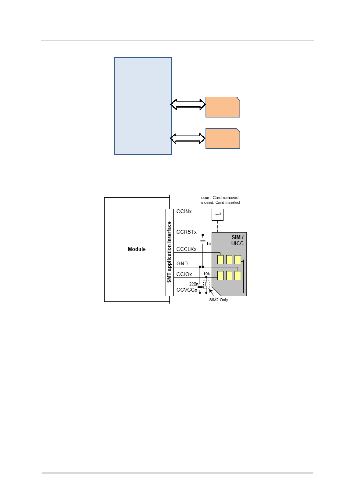
2.1.4 UICC/SIM/USIM Interface
PLS63-W has two UICC/SIM/USIM interfaces (includes eSIM interface) compatible with the
3GPP 31.102 and ETSI 102 221. These are wired to the host interface in order to be connected
to an external SIM card holder. Five pads on the SMT application interface are reserved for
each of the two SIM interfaces.
The UICC/SIM/USIM interface supports 3V and 1.8V SIM cards. Please refer to Table 1 for
electrical specifications of the UICC/SIM/USIM interface lines depending on whether a 3V or
1.8V SIM card is used.
The CCINx signal serves to detect whether a tray (with SIM card) is present in the card holder.
Using the CCINx signal is mandatory for compliance with the GSM 11.11 recommendation if
the mechanical design of the host application allows the user to remove the SIM card during
operation.
Note: No guarantee can be given, nor any liability accepted, if loss of data is encountered after
removing the SIM card during operation. Also, no guarantee can be given for properly initializ-
ing any SIM card that the user inserts after having removed the SIM card during operation. In
this case, the application must restart PLS63-W.
By default, only the module’s 1st SIM interface is available and can be used. The usage of the
module’s 2nd SIM interface has to be configured by AT command.
As an alternative to connecting the module’s two SIM interfaces and switching between these via
AT command, it is possible to connect the first of the module’s SIM interfaces via an external SIM
switch that in turn provides access to a further SIM interface. For details see Section 2.1.4.1.
Table 1: Signals of the SIM interface (SMT application interface)
Signal Description
GND Ground connection for SIM interfaces. Optionally a separate SIM ground line using e.g.,
pad N11, may be used to improve EMC.
CCCLK1
CCCLK2
Chipcard clock lines for 1st and 2nd SIM interface.
CCVCC1
CCVCC2
SIM supply voltage lines for 1st and 2nd SIM interface.
CCIO1
CCIO2
Serial data lines for 1st and 2nd SIM interface, input and output.
CCRST1
CCRST2
Chipcard reset lines for 1st and 2nd SIM interface.
CCIN1
CCIN2
Input on the baseband processor for detecting a SIM card tray in the holder. If the SIM is
removed during operation the SIM interface is shut down immediately to prevent destruc-
tion of the SIM. The CCINx signal is active low.
The CCINx signal is mandatory for applications that allow the user to remove the SIM card
during operation.
The CCINx signal is solely intended for use with a SIM card. It must not be used for any
other purposes. Failure to comply with this requirement may invalidate the type approval of
PLS63-W.
Cinterion®PLS63-W Hardware Interface Overview
2.1 Application Interface
31
tPLS63-W_HIO_v00.860 2021-02-18
Confidential / Preliminary
Page 16 of 61
Figure 5: Module’s two UICC/SIM/USIM interfaces
.
Figure 6: UICC/SIM/USIM interfaces connected
The total cable length between the SMT application interface pads on PLS63-W and the pads
of the external SIM card holder must not exceed 100mm in order to meet the specifications of
3GPP TS 51.010-1 and to satisfy the requirements of EMC compliance.
To avoid possible cross-talk from the CCCLKx signal to the CCIOx signal be careful that both
lines are not placed closely next to each other. A useful approach is using the GND line to
shield the CCIOx line from the CCCLKx line.
SIM1
1st SIMinterface
SIM2
Module
2nd SIMinterface

Cinterion®PLS63-W Hardware Interface Overview
2.1 Application Interface
31
tPLS63-W_HIO_v00.860 2021-02-18
Confidential / Preliminary
Page 17 of 61
2.1.4.1 SIM_SWITCH Line
As an alternative to connecting the module’s two SIM interfaces and switching between these
interfaces by means of AT command, it is possible to connect the first of the module’s SIM in-
terfaces via an external SIM switch that in turn provides access to a further SIM interface.
Figure 7: External UICC/SIM/USIM switch
The module’s GPIO26 line can in this case be configured as SIM_SWITCH line in order to con-
trol the external SIM switch as shown in the sample circuit in Figure 8. A low state would then
indicate the usage of the first SIM interface (SIM1A), a high state would indicate the usage of
the second interface (SIM1B).
The configuration of the SIM_SWITCH (GPIO26) line is done via AT command, is non-volatile,
and available after the next module restart.
Figure 8: Sample circuit for SIM interface connection via SIM switch
SIM1A
Switch
GPIO26/
SIM_SWITCH
SIM1B
Module
1st SIMinterface
ESD
protection
SIM1A
SIM1B
Sim Switch
VSIM1
CCCLK1
CCIO1
CCRST1
SIM_
SWITCH
CCIN1
IF1
COMMON
SIMSELECT
VBAT
External Application Module
ESD
protection IF2
100k
22k
10k
FSA2567
Cinterion®PLS63-W Hardware Interface Overview
2.1 Application Interface
31
tPLS63-W_HIO_v00.860 2021-02-18
Confidential / Preliminary
Page 18 of 61
2.1.5 GPIO Interface
The following table shows the configuration variants for the GPIO pads. All variants are mutu-
ally exclusive, i.e. a pad configured for instance as Status LED is locked for alternative usage.
2.1.6 Digital Audio Interface
PLS63-W supports one digital audio interface that can be deployed as PCM. Inter_IC Sound
(I2S) interface is under development.
2.1.6.1 Pulse Code Modulation Interface
PLS63-W’s PCM interface can be used to connect audio devices capable of pulse code
modulation. The PCM functionality is limited to the use of wideband codec with 16kHz sample
rate only. The PCM interface runs at 16kHz sample rate (62.5μs frame length), while the
signal processing maintains this rate in a wideband AMR call or samples automatically down
Table 2: GPIO lines and possible alternative assignment
GPIO Fast
Shutdown
Status LED ASC0 ASC1 SIM
SWITCH
DAI
GPIO1 DTR0
GPIO2 DCD0
GPIO3 DSR0
GPIO4 FST_SHDN
GPIO5 Status LED
GPIO6
GPIO7
GPIO8
GPIO11
GPIO12
GPIO13
GPIO14
GPIO15
GPIO16 RXD1
GPIO17 TXD1
GPIO18 RTS1
GPIO19 CTS1
GPIO20 DOUT
GPIO21 DIN
GPIO24 RING0
GPIO25
GPIO2 6 SIM_SWITCH
Cinterion®PLS63-W Hardware Interface Overview
2.1 Application Interface
31
tPLS63-W_HIO_v00.860 2021-02-18
Confidential / Preliminary
Page 19 of 61
to 8kHz in a narrowband call. Therefore, the PCM sample rate is independent of the audio
bandwidth of the call.
The PCM interface has the following characteristics:
• Master mode
• Long frame synchronization
• 16kHz/8kHz sample rate
• 512 kHz bit clock at 16kHz sample rate
• 256 kHz bit clock at 8kHz sample rate
Table 3 lists the available PCM interface signals.
Note: PCM data is always formatted as 16-bit uncompressed two’s complement. Also, all
PCM data and frame synchronization signals are written to the PCM bus on the rising clock
edge and read on the falling edge.
2.1.6.2 Inter-IC Sound Interface (TBD)
The I2S Interface is a standardized bidirectio zonal I2S based digital audio interface for trans-
mission of mono voice signals for telephony services.
The I2S properties and capabilities comply with the requirements lay out in the Phillips I2S
Bus Specifications, revised June 5, 1996.
The I2S interface has the following characteristics:
• Bit clock mode: Master
• Sampling rate: 8kHz (narrowband), 16kHz (wideband)
• 256kHz bit clock at 8kHz sample rate
• 512kHz bit clock at 16kHz sample rate
Table 3: Overview of PCM pin functions
Signal name Signal direction
master
Description
DOUT O PCM Data from PLS63-W to external codec.
DIN I PCM Data from external codec to PLS63-W.
FSC O Frame synchronization signal to external codec.
BCLK O Bit clock to external codec. Note: If the BCLK2 signal is
permanently
provided (AT^SAIC parameter <clk_mode> = 0), the
module will no
longer enter its power save (SLEEP) state.
MCLK - Audio master clock. Be synchronous to BCLK to use in
external codec. Can be switched on and off.

Cinterion®PLS63-W Hardware Interface Overview
2.1 Application Interface
31
tPLS63-W_HIO_v00.860 2021-02-18
Confidential / Preliminary
Page 20 of 61
Table 4 lists the available I2S interface signals
2.1.7 Control Signals
2.1.7.1 Status LED
The GPIO5 interface line can be configured to drive a status LED that indicates different oper-
ating mode (for GPIOs see 2.1.5). GPIO and LED functionality are mutually exclusive.
To take advantage of this function connect an LED to the GPIO5/STATUS line as shown in
Figure 9
Figure 9: Status signaling with LED driver
Table 4: Overview of I2S pin functions
Signal name on
SMT application
interface
Signal configura-
tion inactive
Signal direction
Master
Description
DOUT PD O I2S data from PLS63-W to external
codec
DIN PD I I2S data from external codec to
PLS63-W
FSC PD O Frame synchronization signal to/
from external codec Word align-
ment (WS)
BCLK PU O Bit clock to external codec.
BCLK signal low/high time varies
between 45% and 55% of its clock
period.
VCC
STATUS
LED
GNDGND
R1
R2
R3
This manual suits for next models
1
Table of contents
Popular Recording Equipment manuals by other brands


FINEGEAR
FINEGEAR ARKIVE EFFECTS The Dust Collector user manual

JK Audio
JK Audio ComPack user guide

Panasonic
Panasonic WJHD309A - DIGITAL DISK RECORDER Network operating instructions

TC-Helicon
TC-Helicon Play Electric manual

Alesis
Alesis MASTERLINK ML-9600 Reference manual

Precision Power
Precision Power PCE-440 Operator's manual