Thales Cinterion MV31-W User manual
Cinterion®5G M.2 Data Card
MV31-W
Hardware Interface Description
Version: 01.009a
DocId: MV31-W_HID_v01.009a

GENERAL NOTE
THIS DOCUMENT CONTAINS INFORMATION ON THALES PRODUCTS. THALES RESERVES THE
RIGHT TO MAKE CHANGES TO THE PRODUCTS DESCRIBED HEREIN. THE SPECIFICATIONS IN
THIS DOCUMENT ARE SUBJECT TO CHANGE AT THE DISCRETION OF THALES. THE PRODUCT
AND THIS DOCUMENT ARE PROVIDED ON AN "AS IS" BASIS ONLY AND MAY CONTAIN DEFICIEN-
CIES OR INADEQUACIES. THALES DOES NOT ASSUME ANY LIABILITY FOR INFORMATION PRO-
VIDED IN THE DOCUMENT OR ARISING OUT OF THE APPLICATION OR USE OF ANY PRODUCT
DESCRIBED HEREIN.
THALES GRANTS A NON-EXCLUSIVE RIGHT TO USE THE DOCUMENT. THE RECIPIENT SHALL
NOT COPY, MODIFY, DISCLOSE OR REPRODUCE THE DOCUMENT EXCEPT AS SPECIFICALLY
AUTHORIZED BY THALES.
Copyright © 2022, THALES DIS AIS Deutschland GmbH
Trademark Notice
Thales, the Thales logo, are trademarks and service marks of Thales and are registered in certain coun-
tries.
PCI-SIG®, PCIe®and the PCI Express®design mark are registered trademarks and/or service marks of
PCI-SIG.
Microsoft and Windows are either registered trademarks or trademarks of Microsoft Corporation in the
United States and/or other countries.
All other registered trademarks or trademarks mentioned in this document are property of their respective
owners.
tMV31-W_HID_v01.009a 2022-04-27
Public / Preliminary
Cinterion®MV31-W Hardware Interface Description
2
Page 2 of 76
Document Name:
5G M.2 Data Card MV31-W
Version: 01.009a
Date: 2022-04-27
DocId: MV31-W_HID_v01.009a
Status Public / Preliminary
Supported products: FR1 Sub 6 variants (See Section 1.1)

Cinterion®MV31-W Hardware Interface Description
Contents
76
tMV31-W_HID_v01.009a 2022-04-27
Public / Preliminary
Page 3 of 76
Contents
0 Document History ...................................................................................................... 7
1 Introduction ............................................................................................................... 11
1.1 Ordering Information ........................................................................................ 11
1.2 Related Documents ......................................................................................... 12
1.3 Terms and Abbreviations ................................................................................. 12
2 Product Concept ....................................................................................................... 14
2.1 Key Features at a Glance ................................................................................ 15
2.2 System Overview ............................................................................................. 17
2.3 Mechanical Dimensions ................................................................................... 18
3 Application Connector Interface.............................................................................. 20
3.1 Pin Assignments and Electrical Description..................................................... 20
3.2 Characteristics ................................................................................................. 27
3.2.1 Power Supply and Ground.................................................................. 27
3.2.2 Control Signals.................................................................................... 27
3.2.2.1 W_DISABLE1#, W_DISABLE2# Signals ............................ 27
3.2.2.2 RESET# .............................................................................. 27
3.2.2.3 FULL_CARD_POWER_OFF# ............................................ 27
3.2.2.4 WAKE_ON_WWAN#........................................................... 27
3.2.3 Tunable Antenna Interface.................................................................. 29
3.2.3.1 Antenna Control .................................................................. 29
3.2.3.2 ANT_TUNER_CONFIG....................................................... 29
3.2.4 WWAN/WiFi Coexistence Control....................................................... 30
3.2.5 Dynamic Power Reduction.................................................................. 30
3.2.6 USB Interface...................................................................................... 31
3.2.6.1 USB 2.0 Interface................................................................ 31
3.2.6.2 USB 3.1 Gen 2 Interface ..................................................... 31
3.2.7 PCI Express® Interface ...................................................................... 32
3.2.7.1 PERST# Signal ................................................................... 32
3.2.8 SIM/UICC Interface............................................................................. 33
3.2.8.1 ESD Protection for SIM Interfaces ...................................... 34
3.2.9 eUICC Interface .................................................................................. 34
3.2.10 GPIO Interface .................................................................................... 34
3.2.11 Status.................................................................................................. 35
3.2.12 Add-in Card Configuration Pins .......................................................... 35
4 Antenna Interface...................................................................................................... 37
4.1 Antenna Interface Specification ....................................................................... 38
4.1.1 GNSS Interface Characteristics .......................................................... 42
4.2 Antenna Interface Connector ........................................................................... 43
4.2.1 UMTS/LTE & Sub 6G Antenna Connectors........................................ 43

Cinterion®MV31-W Hardware Interface Description
Contents
76
tMV31-W_HID_v01.009a 2022-04-27
Public / Preliminary
Page 4 of 76
5 Operation ................................................................................................................... 44
5.1 Operating Modes ............................................................................................. 44
5.2 Operating Temperatures.................................................................................. 44
5.3 Thermal Design Guidelines.............................................................................. 45
5.3.1 Thermal Solutions ............................................................................... 46
5.4 Power Supply Ratings...................................................................................... 49
5.5 Timing Sequence Requirement ....................................................................... 54
5.5.1 Power On Timing Requirement........................................................... 54
5.5.2 Power Off Timing Requirement........................................................... 56
5.5.3 Power Off Timing ................................................................................ 58
5.5.4 Warm Boot Restart Timing.................................................................. 59
5.5.5 Modem Standby Requirement ............................................................ 59
5.6 Electrostatic Discharge .................................................................................... 62
5.7 Reliability Characteristics ................................................................................. 63
5.8 Mounting Advice .............................................................................................. 64
5.9 Approval Information........................................................................................ 65
5.9.1 Directives and Standards.................................................................... 65
5.9.2 IEC 62368-1 Classification.................................................................. 68
5.9.3 SAR requirements specific to portable mobiles .................................. 69
5.9.4 Reference Equipment for Type Approval............................................ 70
5.9.5 Compliance with FCC and ISED Rules and Regulations.................... 71
5.9.6 Compliance with Japanese Rules and Regulations............................ 71
5.10 Safety Precaution Notes .................................................................................. 72
6 Appendix.................................................................................................................... 73
6.1 Product Label Information................................................................................ 73
6.2 Packaging ........................................................................................................ 74
6.2.1 Trays ................................................................................................... 74
6.3 Declaration of Conformity ................................................................................ 75

Cinterion®MV31-W Hardware Interface Description
Tab l es
76
tMV31-W_HID_v01.009a 2022-04-27
Public / Preliminary
Page 5 of 76
Tables
Table 1: 5G Modem Card Variants .............................................................................. 11
Table 2: Pin assignments............................................................................................. 20
Table 3: Electrical description of connector interface pins ........................................... 23
Table 4: FULL_CARD_POWER_OFF# States ............................................................ 27
Table 5: ANT_TUNER_CONFIG States ...................................................................... 29
Table 6: Coexistence Control between LAA and n79 with WiFi 5GHZ ........................ 30
Table 7: Dynamic Power Reduction States.................................................................. 30
Table 8: Signals of the SIM interface ........................................................................... 33
Table 9: Status States.................................................................................................. 35
Table 10: Add-in Card Configuration.............................................................................. 35
Table 11: GPIO Signals Mapping for Port Configuration 2 ............................................ 36
Table 12: LTE& 5GNR Sub 6G antenna specifications ................................................. 37
Table 13: RF antenna interface LTE: Conductive minimum receiver
input sensitivity (dBm).................................................................................... 38
Table 14: RF antenna interface FR1 (Sub 6G): Conductive minimum receiver
input sensitivity (dBm).................................................................................... 39
Table 15: Antenna interfaces ......................................................................................... 40
Table 16: GNSS properties............................................................................................ 42
Table 17: Temperature characteristics........................................................................... 44
Table 18: 3 Level Throttling Mechanism ........................................................................ 45
Table 19: LTE current consumption ratings ................................................................... 49
Table 20: EN-DC current consumption ratings .............................................................. 52
Table 21: LTE CA current consumption ratings ............................................................. 53
Table 22: Power up timing information........................................................................... 54
Table 23: Power On information .................................................................................... 55
Table 24: Power Off information .................................................................................... 58
Table 25: Warm boot restart information........................................................................ 59
Table 26: Electrostatic values ........................................................................................ 62
Table 27: Summary of reliability test conditions............................................................. 63
Table 28: Directives ....................................................................................................... 65
Table 29: Standards of North American type approval .................................................. 65
Table 30: Standards of European type approval............................................................ 65
Table 31: Standards (Statutory Instruments) for UK...................................................... 66
Table 32: Requirements of quality ................................................................................. 66
Table 33: Standards of the Ministry of Information Industry of the
People’s Republic of China............................................................................ 67
Table 34: Toxic or hazardous substances or elements with defined concentration
limits............................................................................................................... 67
Table 35: IEC 62368-1 Classification............................................................................. 68
Table 36: 5G M.2 Data Card MV31-W label information................................................ 73

Cinterion®MV31-W Hardware Interface Description
Figures
tMV31-W_HID_v01.009a 2022-04-27
Public / Preliminary
Page 6 of 76
Figures
Figure 1: 5G M.2 Data Card MV31-W top view............................................................. 14
Figure 2: 5G M.2 Data Card MV31-W bottom view....................................................... 14
Figure 3: 5G M.2 Data Card MV31-W system overview ............................................... 17
Figure 4: 5G M.2 Data Card MV31-W Dimensions ....................................................... 18
Figure 5: 5G M.2 Data Card MV31-W Ground area (with gold plating) on bottom side 18
Figure 6: 5G M.2 Data Card MV31-W bottom shield dimensions ................................. 18
Figure 7: 5G M.2 Data Card MV31-W on application board (height) [3] ....................... 19
Figure 8: Wake-up scenario .......................................................................................... 28
Figure 9: Wake-up signal .............................................................................................. 28
Figure 10: Typical Wake up schematic ........................................................................... 28
Figure 11: Sample Antenna Tuner with QAT3555 for one antenna path ........................ 29
Figure 12: USB Interface................................................................................................. 31
Figure 13: PCIe® Interface ............................................................................................. 32
Figure 14: SIM Detection Circuit ..................................................................................... 33
Figure 15: SIM interfaces - enhanced ESD protection.................................................... 34
Figure 16: Sample Circuit for Status LED ....................................................................... 35
Figure 17: Antenna Interfaces......................................................................................... 41
Figure 18: UMTS/LTE & Sub 6G Antenna Connector (male).......................................... 43
Figure 19: UMTS/LTE & Sub 6G Antenna Connector (mated plug)................................ 43
Figure 20: Option 1 - Heat sink on top of stepped shielding and
bottom of application PCB.............................................................................. 46
Figure 21: Option 2 - Heat sink only on heat spot of stepped shielding and
bottom of application PCB.............................................................................. 47
Figure 22: Option 3 - Heat sink on top of stepped shielding and directly on
bottom of M.2 card PCB................................................................................. 47
Figure 23: Option 4 - Heat pipe and small application housing....................................... 47
Figure 24: Option 5 - Heat pipe and big application housing .......................................... 48
Figure 25: Thermal distribution with a heat pipe ............................................................. 48
Figure 26: Power-up timing sequence............................................................................. 54
Figure 27: Power on timing diagram ............................................................................... 55
Figure 28: Device power off behavior for Windows 10.................................................... 56
Figure 29: Device power off behavior for Linux............................................................... 57
Figure 30: Power off diagram.......................................................................................... 58
Figure 31: Warm boot restart diagram ............................................................................ 59
Figure 32: Modern Standby-D3cold Entry Flow .............................................................. 60
Figure 33: Modern Standby D3cold................................................................................. 61
Figure 34: Mounting Advice............................................................................................. 64
Figure 35: Reference equipment for type approval......................................................... 70
Figure 36: Sample Label of MV31-W .............................................................................. 73
Figure 37: 5x2 Tray ......................................................................................................... 74

Cinterion®MV31-W Hardware Interface Description
0 Document History
10
tMV31-W_HID_v01.009a 2022-04-27
Public / Preliminary
Page 7 of 76
0 Document History
Preceding document: Cinterion
®
MV31-W Hardware Interface Description, Version 01.009
New document: Cinterion
®
MV31-W Hardware Interface Description, Version
01.009a
Preceding document: Cinterion
®
MV31-W Hardware Interface Description, Version 00.058c
New document: Cinterion
®
MV31-W Hardware Interface Description, Version 01.009
Preceding document: Cinterion
®
MV31-W Hardware Interface Description, Version 00.058b
New document: Cinterion
®
MV31-W Hardware Interface Description, Version 00.058c
Chapter What is new
2.3 Revised Figure 7 showing H2.3-S5 dimensions.
3.1 Updated electrical characteristics for FULL_CARD_POWER_OFF# (Table 3).
3.2.7 Updated Figure 13 to include second PCIe interface lane.
3.2.8.1 Revised Figure 15 to update enhanced ESD protection for SIM interface
3.2.9 New Section eUICC Interface.
4.1 Added notes regarding usage of antenna interfaces.
5.3 Revised thermal design guidelines.
Chapter What is new
2.1 Revised supported 5G bands with DSS.
Revised SIM feature description (DSSS -> DSSA).
2.3 Added 2.3 bottom shield dimensions.
5.2 Added thermal resistance value to Table 17.
5.9 Updated complete approval section.
6New Appendix with label, packaging and conformance information.
Chapter What is new
2.1 Revised PCIe features.
Revised 5G/4G category features.
2.2 Revised Figure 3 to add optional UIM card holder.
3.1 Updated some electrical descriptions in Table 3.
3.2.2.3 Added note recommending >30s pause between powering off and on again.
4.1 Revised Table 13, Table 14, and Table 15.
5.4 Added remark regarding recommended power reserve for peak current consumption.
6 Removed Appendix with tables showing supported CA and EN-DC configurations.
These configurations are now listed in a dedicated User Guide (see [2]).

Cinterion®MV31-W Hardware Interface Description
0 Document History
10
tMV31-W_HID_v01.009a 2022-04-27
Public / Preliminary
Page 8 of 76
Preceding document: Cinterion
®
MV31-W Hardware Interface Description, Version 00.058a
New document: Cinterion
®
MV31-W Hardware Interface Description, Version 00.058b
Preceding document: Cinterion
®
MV31-W Hardware Interface Description, Version 00.058
New document: Cinterion
®
MV31-W Hardware Interface Description, Version 00.058a
Preceding document: Cinterion
®
MV31-W Hardware Interface Description, Version 00.057a
New document: Cinterion
®
MV31-W Hardware Interface Description, Version 00.058
Preceding document: Cinterion
®
MV31-W Hardware Interface Description, Version 00.057
New document: Cinterion
®
MV31-W Hardware Interface Description, Version 00.057a
Chapter What is new
3.2.7.1 Revised description of PERST# signal
3.2.8 Added Figure 14 SIM Detection Circuit
Chapter What is new
-- Removed n40
2.1 Added Data Throughput and Bands supporting DSS
4.1 Revised Table 15 regarding 5G Sub6 TX
5.2 Added Thermal Throttling Thresholds in Table 17
5.3 Added Table 18 for 3 Level Throttling Mechanism
Chapter What is new
3.1 Changed Table 2 and Table 3 regarding to WAKE_ON_WWAN# signal
3.2.2.4 Revised chapter WAKE_ON_WWAN# signal is now supported
Chapter What is new
1.1 Revised Table 1 regarding eSIM information
2.1 Added PCB tolerance at maximum height and revised description of SIM and SIM inter-
face
2.2 Revised Figure 3 regarding 2nd SIM Interface
3.1 Revised Table 2 regarding UIM_1 and Table 3 regarding MIPI interface
3.2.2.1 Revised chapter regarding control circuit
3.2.3.2 Revised chapter
3.2.7 Revised Design Guidelines and Figure 13
3.2.8 Added information that 2nd interface is reserved for future use
3.2.8.1 Changed sample ESD protection component to NUP4114 and added capacitors
5.5 Replaced baseband chip name by product name
5.8 Added Chapter for Mounting Advice

Cinterion®MV31-W Hardware Interface Description
0 Document History
10
tMV31-W_HID_v01.009a 2022-04-27
Public / Preliminary
Page 9 of 76
Preceding document: Cinterion®MV31-W Hardware Interface Description, Version 00.050
New document: Cinterion
®
MV31-W Hardware Interface Description, Version 00.057
Preceding document: Cinterion
®
MV31-W Hardware Interface Description, Version 00.007
New document: Cinterion
®
MV31-W Hardware Interface Description, Version 00.050
Preceding document: Cinterion
®
MV31-W Hardware Interface Description, Version 00.006
New document: Cinterion
®
MV31-W Hardware Interface Description, Version 00.007
Preceding document: Cinterion
®
MV31-W Hardware Interface Description, Version 00.005
New document: Cinterion
®
MV31-W Hardware Interface Description, Version 00.006
Chapter What is new
2.1, 3.1 Changed maximum supply voltage to 4.8V.
5.7 Revised Table 27 Summary of reliability test conditions.
6.2 Revised Table 38 EN-DC Configurations.
Chapter What is new
Throughout
document
Removed details about mmWave antenna connectors as mmWave bands are not sup-
ported with this product variant.
2Revised Figure 1 and Figure 2 showing MV31-W top and bottom view.
3.1 Revised signal properties in Table 2.
3.2.5 Added resistor value to Figure 16.
4.1.1 Added GNSS frequencies.
5.2 Added max temperature for automatic thermal shutdown.
5.6 Revised ESD information.
6.1 Removed some comments supported CA configuration tables.
Chapter What is new
5.4 Revised power supply ratings.
5.5 Added timing Sequence Requirement together with its subsections.
6 New Appendix with Supported LTE CA Configurations and Supported EN-DC Configu-
rations.
Chapter What is new
2.1 Revised supported Bands.
2.1, 3.1, 5.4 Changed lowest supply voltage to 3.14V (Table 3).
3.1 Revised Table 2 column Pin Type.
3.2.6 Revised USB interface description.
4Revised notes of Table 12.
Cinterion®MV31-W Hardware Interface Description
0 Document History
10
tMV31-W_HID_v01.009a 2022-04-27
Public / Preliminary
Page 10 of 76
Preceding document: Cinterion
®
MV31-W Hardware Interface Description, Version 00.004
New document: Cinterion
®
MV31-W Hardware Interface Description, Version 00.005
Preceding document: Cinterion
®
MV31-W Hardware Interface Description, Version 00.003
New document: Cinterion
®
MV31-W Hardware Interface Description, Version 00.004
Preceding document: Cinterion
®
MV31-W Hardware Interface Description, Version 00.002
New document: Cinterion
®
MV31-W Hardware Interface Description, Version 00.003
Preceding document: Cinterion
®
MV31-W Hardware Interface Description, Version 00.001
New document: Cinterion
®
MV31-W Hardware Interface Description, Version 00.002
New document:
Cinterion
®
MV31-W Hardware Interface Description, Version 00.001
Chapter What is new
--- Removed information about FR2 bands.
Chapter What is new
--- Removed information about mmWave Variants.
2.1 Revised supported bands.
Chapter What is new
3RESET# is not supported.
3.1 Added characteristics in Table 3 for mmWave_1P85.
3.2.3.1 Added Antenna Tuner example (Figure 11).
3.2.4, 3.2.5 Signal description improved.
4.1 Revised Table 13.
4.1.1 Revised Table 16.
5.3 Inserted new chapter Thermal Design Guidelines.
Chapter What is new
2.3 Added information about M.2 Application Connector.
2.3 Figure 7: Thermal Pad added.
3WAKE_ON_WWAN# is not supported.
32nd PCI lane added for future use.
3Change signal direction for signals mmWave_Enable_x in Table 2 and Table 3.
3.2.3 Revised signal description.
Chapter What is new
-- Initial document setup.

Cinterion®MV31-W Hardware Interface Description
1 Introduction
75
tMV31-W_HID_v01.009a 2022-04-27
Public / Preliminary
Page 11 of 76
1 Introduction
This document1describes the hardware of the Cinterion®5G M.2 Data Card MV31-W product.
It helps you quickly retrieve interface specifications, electrical and mechanical details, and in-
formation on the requirements to be considered for integrating further components.
CAUTION: M.2 Add-in Card are not designed or intended to support Hot-Swap or Hot-Plug
connections. Performing Hot-Swap or Hot-Plug may pose danger to the M.2 Add-in Card, to
the system Platform, and to the person performing this act.
1.1 Ordering Information
Where necessary a note is made to differentiate between the various product variants.
1. The document is effective only if listed in the appropriate Release Notes as part of the technical docu-
mentation delivered with your Thales product.
Table 1: 5G Modem Card Variants
Product Interface Band Support eSIM Ordering information
MV31-W USB 3.1
USB 2.0
FR1 (Sub 6)
Yes Packaging unit (ordering) number:
L30960-N6910-A100
Module label number1:
S30960-S6910-A100
1. Note: At the discretion of Thales, module label information can either be laser engraved on the module’s
shielding or be printed on a label adhered to the module’s shielding.
MV31-W USB 3.1
USB 2.0
FR1 (Sub 6)
No Packaging unit (ordering) number:
L30960-N6910-B100
Module label number1:
S30960-S6910-B100
MV31-W PCIe®
(2xlane)
USB 2.0
FR1 (Sub 6)
Yes Packaging unit (ordering) number:
L30960-N6920-A100
Module label number1:
S30960-S6920-A100
MV31-W PCIe®
(2xlane)
USB 2.0
FR1 (Sub 6)
No Packaging unit (ordering) number:
L30960-N6920-B100
Module label number1:
S30960-S6920-B100
Starter Kit 5G Data Card USB
FR1 (Sub 6)
Packaging unit (ordering) number:
L30960-N6901-A100
Module label number1:
S30960-S6901-A100
Starter Kit 5G Data Card PCIe®
FR1 (Sub 6)
Packaging unit (ordering) number:
L30960-N6902-A100
Module label number1:
S30960-S6902-A100

Cinterion®MV31-W Hardware Interface Description
1.2 Related Documents
75
tMV31-W_HID_v01.009a 2022-04-27
Public / Preliminary
Page 12 of 76
1.2 Related Documents
[1] MV31-W Release Note
[2] MV31-W Band Combination Configuration User Guide
[3] PCI Express®M.2 Specification, Revision 4.0, November 5, 2020, PCI-SIG
[4] PCI Express®Card Electromechanical Specification, Revision 1.1, March 28, 2005
[5] Universal Serial Bus Specification1, Revision 2.0,April 27, 2000, USB.ORG
[6] Universal Serial Bus 3.2 Specification2September 22, 2017, USB 3.0 Promoter Group
1.3 Terms and Abbreviations
1. The specification is available for download on http://www.usb.org/developers/docs/
Abbreviation Description
3FF Third Form Factor
3GPP 3rd Generation Partnership Project
CE Conformité Européene (European Conformity)
CSD Circuit Switched Data
CTM Cellular Text Telephone Modem
DSS Dynamic Spectrum Sharing
EN-DC E-UTRAN New Radio Dual Connectivity
ETS European Telecommunication Standard
FCC Federal Communications Commission (U.S.)
GPRS General Packet Radio Service
GSM Global Standard for Mobile Communications
HPUE High Power User Equipment
HSPA High Speed Packet Access
HSDPA High Speed Download Packet Access
I/O Input/Output
IC Integrated Circuit
IEC International Electrotechnical Commission
ISO International Standards Organization
ITU International Telecommunications Union
LAA Licensed Assisted Access
LED Light Emitting Diode
Mbps Mbits per second
MFF2 M2M UICC Form Factor 2
MMI Man Machine Interface
MNO Mobile Network Operator

Cinterion®MV31-W Hardware Interface Description
1.3 Terms and Abbreviations
75
tMV31-W_HID_v01.009a 2022-04-27
Public / Preliminary
Page 13 of 76
MO Mobile Originated
MT Mobile Terminated
PBCCH Packet Switched Broadcast Control Channel
PCI Peripheral Component Interconnect (personal computer bus)
PDU Protocol Data Unit
PIN Personal Identification Number
PPP Point-to-point protocol
R&TTE Radio and Telecommunication Terminal Equipment
RF Radio Frequency
RFFE RF Front End
RLP Radio Link Protocol
RoHS Restriction of the use of certain hazardous substances in electrical and electronic
equipment.
S4 Microsoft Windows power state for Hibernation.
S5 Microsoft Windows power state for Soft (power) Off.
SAR Specific Absorption Rate
SIM Subscriber Identification Module
SMS Short Message Service
TTY Text Telephone
UICC Universal Integrated Circuit Card
UMTS Universal Mobile Telecommunications System
USB Universal Serial Bus
USSD Unstructured Supplementary Service Data
Abbreviation Description
Cinterion®MV31-W Hardware Interface Description
2 Product Concept
75
tMV31-W_HID_v01.009a 2022-04-27
Public / Preliminary
Page 14 of 76
2 Product Concept
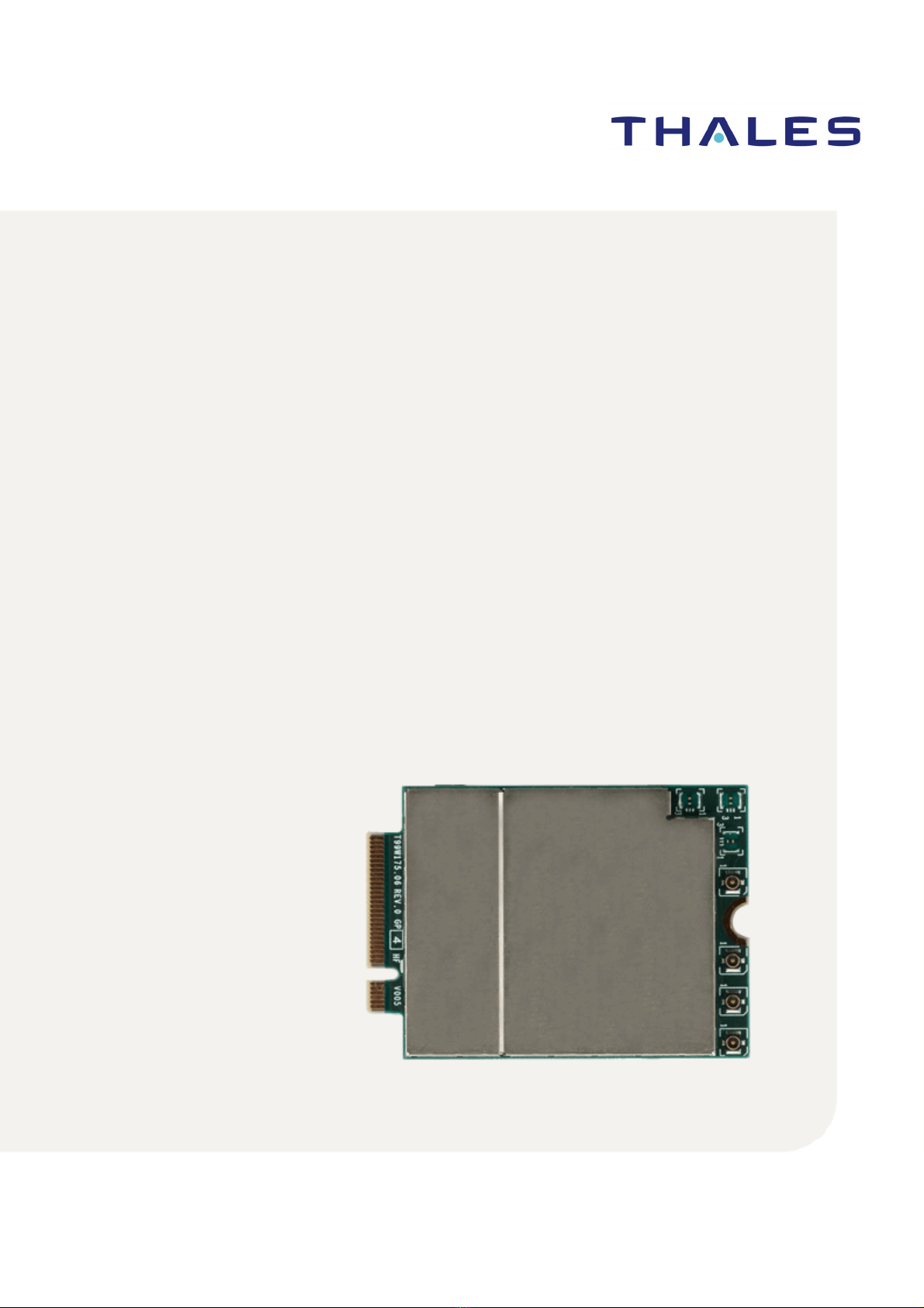
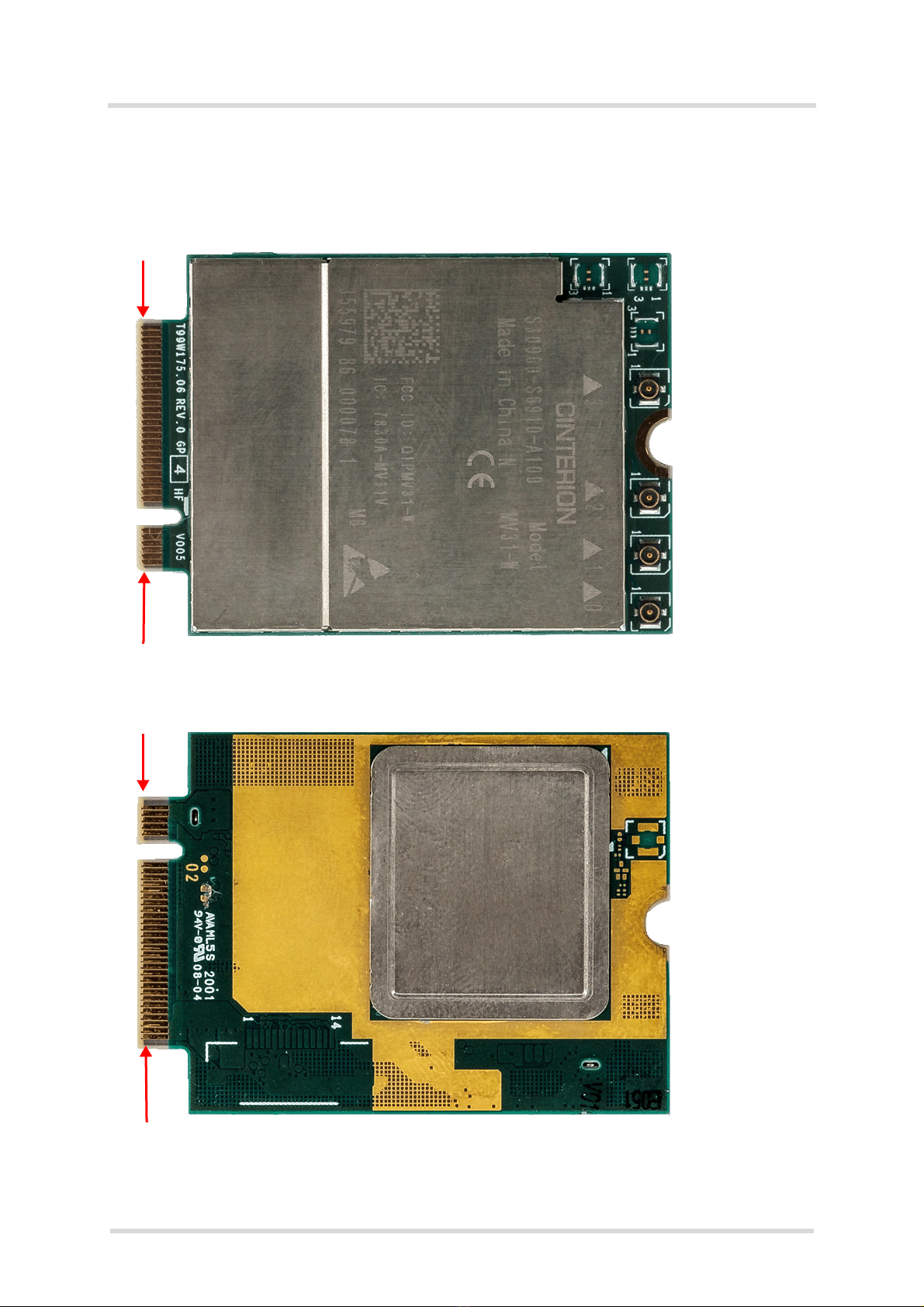
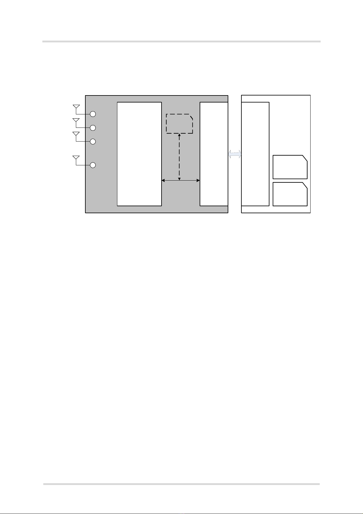
Figure 1 shows the top view and Figure 2 the bottom view of 5G M.2 Data Card MV31-W.
Figure 1: 5G M.2 Data Card MV31-W top view
Figure 2: 5G M.2 Data Card MV31-W bottom view
Mechanical ground pad
Pin 75
Pin 1
Antenna
LTE & Sub 6G RX/TX
Antenna
LTE & Sub 6G RX/GPS L5
Antenna
LTE & Sub 6G RX/TX
Antenna
LTE & Sub 6G RX/GPS L1
Pin 2
Pin 74

Cinterion®MV31-W Hardware Interface Description
2.1 Key Features at a Glance
75
tMV31-W_HID_v01.009a 2022-04-27
Public / Preliminary
Page 15 of 76
2.1 Key Features at a Glance
Feature Implementation
General
Data throughput DL 3.88Gbps (max. theoretical: 4.14 Gbps) at
EN-DC: DC_3C-1A-7C-n78A with LTE 5CA 4x4 MIMO (20 Layers) +
Sub6G 4x4 MIMO
UL 632 Mbps (max theoretical: 660 Mbps) at
(EN-DC: DC_7C-n78A with LTE UL CA + Sub6G SISO)
5G
Bands FR1 (Sub 6G):
FDD: n1, n2, n3, n5, n7, n8, n12, n20, n28, n66, n71
TDD: n38, n41, n77, n78, n79
Band combinations For supported E-UTRAN New Radio Dual Connectivity (EN-DC) see [2]
4x4 MIMO n1, n2, n3, n7, n66, n38, n41, n77, n78, n79
DSS n1, n2, n3, n5, n7, n8, n12, n20, n28, n66, n71
Category 3GPP Rel 15
256 QAM UL/DL
Output Power FR1 (Sub 6G):
n41, n77, n78, n79: 25.5dBm +1.5/-1dB (HPUE)
All other bands: 23dBm ±1dB
4G
Bands FDD: B1, B2, B3, B4, B5, B7, B8, B12, B13, B14, B17, B18, B19, B20, B25,
B26, B28, B29, B30, B32, B66, B71
TDD: B34, B38, B39, B40, B41, B42, B48
LAA: B46 (DL only)
Band combinations For supported carrier aggregations (CA) see [2]
4x4 MIMO B1, B2, B3, B4, B7, B25, B30, B38, B39, B40, B41, B42, B48, B66
RX Diversity All LTE bands
Category UE Cat. 13 (UL: 150Mbps) + UE Cat. 20 (DL: 2Gbps);
7xDL CA, 3xUL CA (Intra-band), 5xDL CA+4X4 MIMO (Up to UE Cat20)
256 QAM UL/DL
Output Power B30: 22dBm ±1dBm
B39: 20dBm (typical), 22.7dBm (maximum) for Japan region
B41: 25.5dBm +1.5/-1.5dBm (HPUE)
B42: 21 ±1dBm for US region
B48: 21 +1dBm/-0.7dBm
B1, B2, B3, B4, B7, B25, B34, B38, B40, B66: 23dBm ±1dBm
B5, B8, B12, B13, B14, B17, B18, B19, B20, B26, B28, B71: 23.5dBm ±1dBm
3G
Bands Bd.I, Bd.II, Bd.IV, Bd.V (Bd.VI, Bd.XIX), Bd.VIII, Bd.IX
RX Diversity All 3G bands
Category DC-HSPA+ – DL Cat. 24 (42Mbps) / UL Cat. 6 (11Mbps)
HSUPA – UL 5.76Mbps
Compressed mode (CM) supported according to 3GPP TS25.212
Output Power All bands: 23.5dBm +1/-1dB
Cinterion®MV31-W Hardware Interface Description
2.1 Key Features at a Glance
75
tMV31-W_HID_v01.009a 2022-04-27
Public / Preliminary
Page 16 of 76
GNSS Dual-Frequency GNSS:
GPS: L1; L5
GLONASS: G1
Beidou: B1
Galileo E1; E5a
SIM Dual SIM with eSIM on board, Dual SIM Single Active (DSSA)
Power supply 3.3V (typical, min. 3.14V,max. 4.8V)
Temperature Normal operation: -30°C to +70°C
Extended operation: -40°C to +85°C
Storage: -40°C to +85°C
Physical Dimensions: 42 mm × 30 mm × 2.6 mm
Weight: approx. 8 g
RoHS All hardware components fully compliant with EU RoHS Directive
Interfaces
Form factor M.2 3042 S3 Key B
Application connector PCI Express®M.2 Card system connector (75 pin golden finger, Key ID B)
USB USB 2.0
MV31-W USB only:
USB 3.1 Gen.2 SuperSpeed (10Gbps)
USB configuration supported:
Windows(TM)10: MBIM, GNSS
Linux: DIAG, MBIM/RmNet, Modem, NMEA
PCIe®MV31-W PCIe®only:
Supports Endpoint and Root Complex, Gen 3, 2 lanes
PCIe®configuration supported:
Windows(TM)10: MBIM, GNSS
Linux: DIAG, MBIM, Modem, NMEA
Driver Windows(TM) 10 / Windows(TM) 10: Supports both PCIe®and USB interfaces
Linux Kernel versions 5.13 / 5.15: MBIM on both PCIe®and USB interfaces
Android 11: RIL driver SW
UICC Supported SIM/USIM cards: 3V, 1.8V
External SIM card reader has to be connected via application connector.
A second SIM/USIM interface is optionally available at the application con-
nector.
Antenna 4 MHF4 type connectors for UMTS/LTE/5G (Sub 6G) main antenna and
UMTS/LTE/5G (Sub 6G) Diversity/MIMO antennas
Feature Implementation
Cinterion®MV31-W Hardware Interface Description
2.2 System Overview
75
tMV31-W_HID_v01.009a 2022-04-27
Public / Preliminary
Page 17 of 76
2.2 System Overview
Figure 3: 5G M.2 Data Card MV31-W system overview
Wireless
Modem
Application
connector
(75 pin)
PC /
Power supply
SIM card
holder
RF antennas
Connector
socket
(75 pin)
MV31
eSIM
(optional )
ANT0
ANT1
ANT2
ANT3
USB
PCIe
UIM card
holder
(optional)

Cinterion®MV31-W Hardware Interface Description
2.3 Mechanical Dimensions
75
tMV31-W_HID_v01.009a 2022-04-27
Public / Preliminary
Page 18 of 76
2.3 Mechanical Dimensions
The mechanical dimensions for PCI Express M.2 Cards with a 3042 form factor are specified
in [3] and shown in Figure 4, Figure 5 and Figure 7.
Figure 4: 5G M.2 Data Card MV31-W Dimensions
Figure 5: 5G M.2 Data Card MV31-W Ground area (with gold plating) on bottom side
Figure 6: 5G M.2 Data Card MV31-W bottom shield dimensions

Cinterion®MV31-W Hardware Interface Description
2.3 Mechanical Dimensions
75
tMV31-W_HID_v01.009a 2022-04-27
Public / Preliminary
Page 19 of 76
The 5G M.2 Data Card MV31-W complies with the single-sided add-in card H2.3-S5: “Stack-
up Top Mount Single-sided Add-in Card for 2.00 Maximum Top-side Component Height and
with Higher Clearance above Motherboard” specified in [3].
Figure 7: H2.3-S5 single-sided add-in card dimensions
The area under the 5G M.2 Data Card on the Application Board should be free of components
and signals, but needs to be part of a thermal solution (see Section 5.3).
values in mm
Cinterion®MV31-W Hardware Interface Description
3 Application Connector Interface
75
tMV31-W_HID_v01.009a 2022-04-27
Public / Preliminary
Page 20 of 76
3 Application Connector Interface
3.1 Pin Assignments and Electrical Description
Table 2 matches the 5G M.2 Data Card MV31-W pin assignments at the 75-pin application con-
nector to the pin assignments specified in [3]. Table 3 lists electrical characteristics of the as-
signed and available pins at the application connector interface.
Table 2: Pin assignments
Pin
No.
5G M.2 Data Card
MV31-W
pin name1
Comments PIN Type
1 CONFIG_3 Add-in Card Configuration 3, Section 3.2.12 Output
3 GND
5 GND
7 USB+ USB Data, Section 3.2.6.1
9 USB-
11 GND
Key ID B
21 CONFIG_0 Add-in Card Configuration 0,Section 3.2.12 Output
23
WAKE_ON_WWAN#
Wake on WWAN, Section 3.2.2.4 Output 1.8V
25 DPR_1 Dynamic Power Reduction (SAR), Section 3.2.5 Input 1.8V
27 GND
29 USB3.1-Tx- USB 3.1 (USB Tx-), Section 3.2.6.2 Output
Usage as PCIe
or USB 3.1 i/f
dependent on
HW variant
PETn1 2nd PCIe®lane Tx-, Section 3.2.7
31
USB3.1-Tx+ USB 3.1 (USB Tx+), Section 3.2.6.2
PETp1 2nd PCIe®lane Tx+, Section 3.2.7
33 GND
35 USB3.1-Rx- USB 3.1 (USB Rx-), Section 3.2.6.2 Input
Usage as PCIe
or USB 3.1 i/f
dependent on
HW variant
PERn1 2nd PCIe®lane Rx-, Section 3.2.7
37
USB3.1-Rx+ USB 3.1 (USB Rx+), Section 3.2.6.2
PERp1 2nd PCIe®lane Rx+, Section 3.2.7
39 GND
41 PETn0 1st PCIe®lane Tx+/-, Section 3.2.7 Output
43 PETp0
45 GND
Table of contents


