THine THCV245 A User manual
Preliminary
THCV245A_Rev.0.90_E
Copyright©2020 THine Electronics, Inc. THine Electronics, Inc.
Security C
1/67
THCV245A
SerDes transmitter with bi-directional transceiver
1General Description
THCV245A is designed to support 1080p60 2Mpixel
uncompressed video data over 15m 100ohm
differential STP or single-end 50ohm Coaxial cable
with 4 in-line connectors between camera and
processor by V-by-One®HS.
THCV245A supports a MIPI CSI-2. Each CSI-2 data
lane can transmit up to 1.2Gbps/lane. Virtual channel
is supported.
THCV245A is particularly targeted to medical and
other applications requiring low power consumption.
One high-speed V-by-One® HS lane can transmit up
to 1080p60fps. The maximum serial data rate is
4Gbps/lane. 2nd output lane supports HDR large
amount of data or data copy-and-distribution
experience.
THCV245A is capable to control and monitor
camera module from remote ECU via GPIO, UART or
1Mbps 2-wire serial interface.
Several fault and error detection function including
CRC provides hardware functional safety design.
2Features
MIPI CSI-2 with 1,2 or 4-lane input
MIPI D-PHY supports 80Mbps~1.2Gbps
MIPI Virtual channel supported
Video formats: RAW8/10/12/14/16/20,
YUV422/420, RGB888/666/565, JPEG, User-
defined generic 8-bit
V-by-One®HS 400Mbps~4Gbps x2lane
V-by-One®HS standard version1.5
Reference clock input CKI range 10~40MHz
shareable with video source CMOS sensor
Wide range IO voltage from 1.7V to 3.6V
Additional spread spectrum to reduce EMI
2-wire serial interface 1Mbps bridge function
Remote GPIO/UART control and monitoring
Error detection including CRC and notification
Low Current Consumption
QFN40 5x5mm 0.4mm pitch Exp-pad package
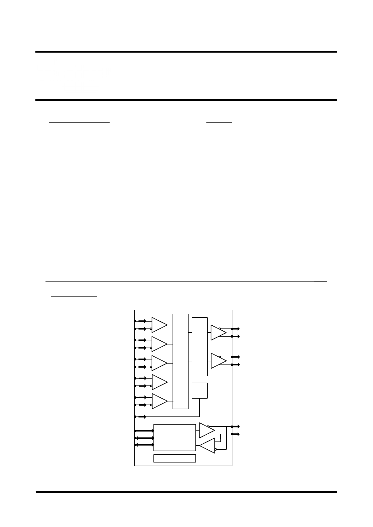
3Block Diagram
RD3p
RD3n
CSI2 / Formatter
SerializerPLL
Controls
RCKp
RCKn
OSC
RD1p
RD1n
Settings
2-wire
serial I/F
TX0N
TX0P
TCMN
TCMP
MIPI CSI-2
Rx 4-lane THCV245A V-by-One® HS
Tx 2 lane
Sub-Link
RD0p
RD0n
RD2p
RD2n
TX1N
TX1P
GPIO
CKI

Preliminary
THCV245A_Rev.0.90_E
Copyright©2020 THine Electronics, Inc. THine Electronics, Inc.
Security C
2/67
Contents Page
1General Description.........................................................................................................................................1
2Features ...........................................................................................................................................................1
3Block Diagram ................................................................................................................................................1
4Pin Configuration............................................................................................................................................4
5Pin Description................................................................................................................................................5
6Functional Description....................................................................................................................................6
6.1 Functional Overview...............................................................................................................................6
6.2 Reference clock supply............................................................................................................................6
6.3 MIPI input setting....................................................................................................................................7
6.4 HTPDN/LOCKN.....................................................................................................................................8
6.5 V-by-One® HS output setting.................................................................................................................9
6.5.1 MPRF (Main-Link PRivate Format) ...............................................................................................9
6.5.2 V-by-One® HS standard format....................................................................................................10
6.5.3 V-by-One® HS output Byte mode.................................................................................................16
6.5.4 V-by-One® HS output Distribution mode.....................................................................................16
6.5.5 V-by-One® HS Low Radiation Emission or High Immunity Resistance mode............................16
6.5.6 V-by-One® HS output Odd/Even swap.........................................................................................17
6.5.7 V-by-One® HS output Drivability ................................................................................................17
6.5.8 V-by-One® HS output Low Frequency mode...............................................................................17
6.5.9 Target Pixel clock..........................................................................................................................18
6.6 Blanking period restriction under low MIPI data-rate environment......................................................18
6.7 PLL setting ............................................................................................................................................19
6.8 PLLAuto setting function .....................................................................................................................22
6.9 V-by-One® HS output data-rate............................................................................................................23
6.10 V-by-One® HS output Spread Spectrum...............................................................................................23
6.11 V-by-One® HS CRC.............................................................................................................................24
6.12 MIPI Packet Header V-by-One® HS output bridge mode ....................................................................25
6.13 MIPI Virtual Channel bridge.................................................................................................................26
6.14 V-by-One® HS VSYNC generation......................................................................................................27
6.15 V-by-One® HS HSYNC generation......................................................................................................28
6.16 MIPI Short Packet V-by-One® HS output bridge mode .......................................................................30
6.17 2-wire serial interface............................................................................................................................32
6.17.1 2-wire serial I/F slave Device ID...................................................................................................32
6.17.2 2-wire serial Read/Write access to local Register..........................................................................33
6.18 2-wire serial I/F Watch Dog Timer........................................................................................................34

Preliminary
THCV245A_Rev.0.90_E
Copyright©2020 THine Electronics, Inc. THine Electronics, Inc.
Security C
3/67
6.19 Register Auto Checksum diagnosis....................................................................................................... 34
6.20 Sub-Link setting ....................................................................................................................................35
6.20.1 Sub-Link 2-wire Set and Trigger mode (2-wire Normal mode)....................................................37
6.21 Sub-Link Watch Dog Timer...................................................................................................................40
6.22 Sub-Link Interrupt detection .................................................................................................................41
6.23 GPIO setting..........................................................................................................................................42
6.23.1 Sub-Link Polling GPIO input/output.............................................................................................42
6.23.2 Register GPIO ...............................................................................................................................44
6.24 Internal Error / status signal monitoring GPIO output ..........................................................................45
6.25 Internal Error / status signal monitoring register...................................................................................46
6.26 Interrupt monitoring ..............................................................................................................................47
6.27 Build-In Self-Test pattern generator (BIST)..........................................................................................49
6.28 Main-Link Field BET............................................................................................................................51
6.29 Sub-Link Field BET operation and output from GPIO .........................................................................51
6.30 CMOS IO Input noise Filter..................................................................................................................52
6.31 CMOS output drive strength .................................................................................................................52
6.32 CKO reference clock buffer output .......................................................................................................53
6.33 Soft Reset ..............................................................................................................................................54
6.34 Power On Sequence...............................................................................................................................56
6.35 Lock / Re-Lock Sequence .....................................................................................................................57
7Absolute Maximum Ratings..........................................................................................................................58
8Recommended Operating Conditions............................................................................................................58
9Consumption Current....................................................................................................................................59
10 DC Specifications......................................................................................................................................60
10.1 CMOS DC Specifications......................................................................................................................60
10.2 MIPI Receiver DC Specifications .........................................................................................................60
10.3 CMLTransmitter DC Specifications.....................................................................................................61
10.4 CML Bi-directional Buffer DC Specifications......................................................................................62
11 AC Specifications..........................................................................................................................................63
11.1 MIPI Receiver AC Specifications..........................................................................................................63
11.2 CMLTransmitter AC Specifications ..................................................................................................... 63
11.3 CML B-directional Buffer AC Specifications .......................................................................................63
11.4 2-wire serial Master/Slave AC Specifications....................................................................................... 64
12 Package......................................................................................................................................................66
13 Notices and Requests.................................................................................................................................67
MIPI is a licensed trademark of MIPI, Inc. in the U.S. and other jurisdictions.

Preliminary
THCV245A_Rev.0.90_E
Copyright©2020 THine Electronics, Inc. THine Electronics, Inc.
Security C
4/67
4Pin Configuration
30 29 28 27 26 25 24 23 22 21
VDDM
SCL
SDA
AIN
INT
VDDL
PDN0
VDDIO
MSSEL
LOCKN
31 RD3P THCV245A VDDA 20
32 RD3N TX0N 19
33 RD1P 41 EXPGND TX0P 18
34 RD1N TX1N 17
35 RCKP TX1P 16
36 RCKN TEST 15
37 RD0P TCMN 14
38 RD0N TCMP 13
39 RD2P PDN1 12
40 RD2N VDDB 11
VDDM
VDDOP
CKO
VDDIO
CKI
VDDL
GPIO0
GPIO1
GPIO2
GPIO3
1 2 3 4 5 6 7 8 9 10

Preliminary
THCV245A_Rev.0.90_E
Copyright©2020 THine Electronics, Inc. THine Electronics, Inc.
Security C
5/67
5 Pin Description
Pin Name Pin # type* Description
RD3P/N 31,32 MI MIPIlane3 differential data input
RD1P/N 33,34 MI MIPIlane1 differential data input
RCKP/N 35,36 MI MIPI differential clock inputs
RD0P/N 37,38 MI MIPIlane0 differential data input
RD2P/N 39,40 MI MIPIlane2 differential data input
TX0P/N 18,19 CO V-by-One® HS lane0 High-speed CML signal output
TX1P/N 16,17 CO V-by-One® HS lane1 High-speed CML signal output
TCMP/N 13,14 CB/B TCMP/N(PDN1=1): CML Bi-directional Input/Output(Sub-Link).
NC (PDN1=0): Not Connected. Must be open.
SCL 29 B 2-wire serial Master/Slave SCL
SDA 28 B 2-w ire serial Master/Slave SDA
PDN0 24 I Whole IC Power Down
0 : Power Down
1 : Normal Operation
PDN1 12 I Sub-Link Power Down
0 : Sub-Link Power Down
1 : Sub-Link Normal Operation
TEST 15 I Test pin. Must be tied to Ground for normal operation.
CKI 5 I Reference Clock Input
CKO 3 O Reference Clock Output
LOCKN 21 I LOCK detect input Negative polarity
If external LOCKNconnection is used, it is supposed to be
connected to Rx LOCKN w ith a 30kΩ pull-up resistor.
GPIO0 7 B GPIO0
GPIO1 8 B GPIO1
GPIO2 9 B GPIO2
GPIO3 10 B GPIO3
MSSEL 22 I
MSSEL (PDN1=1): Sub-Link Master/Slave Select
0 : Sub-Link Master side(inside 2-w ire serial I/F is slave)
1 : Sub-LinkSlave side(inside 2-wire serial I/F is master)
Sub-Link Master is connected to HOST MCU.
HTPDN(PDN1=0): HoT Plug Detect input Negative polarity
Must be connected to Rx HTPDN w ith a 30kΩ pull-up resistor.
AIN 27 I Select Slave Address
0 : 2wire serial Address = 7'b000_1011
1 : 2wire serial Address = 7'b011_0100
INT 26 O
Interrupt signal output.
It must be connected with a pull-up resistor.
0 : Interrupt occurred
1 : Steady state
VDDOP 2 P PLL Power supply Pin 1.2V
VDDM 1,30 P MIPIPower supply Pin 1.2V
VDDA 20 P Analog Power supply Pin 1.2V
VDDL 6,25 P Digital Power supply Pins 1.2V
VDDB 11 P Analog Power supply Pin 1.8~3.3V
VDDIO 4,23 P IO Pow er supply Pin 1.8~3.3V
EXPGND 41 G Exposed Pad Ground : Must be tied to Ground
*type symbol
MI=MIPIInput, CO=CML Output
CB=CML Bi-directional input/output
B=1.8~3.3V CMOS Bi-directional input/output, I=1.8~3.3v CMOS Input, O=1.8~3.3v CMOS Output
P=Power, G=Ground
Preliminary
THCV245A_Rev.0.90_E
Copyright©2020 THine Electronics, Inc. THine Electronics, Inc.
Security C
6/67
6 Functional Description
6.1 Functional Overview
THCV245A can receive MIPI CSI-2 video and transmit it to over 15m length. With High Speed CML SerDes,
high reliability and robustness encoding scheme and CDR (Clock and Data Recovery) architecture, the
THCV245A enables to transmit RAW/YUV/RGB/JPEG/Generic8bit data through Main-Link by single 100ohm
differential pair or 50ohm Coax cable with minimal external components. Maximum supported resolution is
horizontal active 3840 pixels format. In addition, the THCV245A has Sub-Link which enables bi-directional
transmission of 2-wire serial interface signals, GPIO signals and also HTPDN/LOCKN signals for Main-Link
through the other 1-pair of CML-Line. The THCV245A system is able to watch peripheral devices and to control
them via 2-wire serial interface or GPIOs. They also can report interrupt events caused by change of GPIO inputs
and internal statuses such as CRC error.
6.2 Reference clock supply
Reference clock supply CKI is required since MIPI CSI-2 clock stream will not always be continuous.
CKI frequency examples are 24MHz, 27MHz and 37.125MHz.
To supply the same oscillator clock as CMOS sensor to THCV245A is recommended.
See Figure 1.
Physical layout artwork of oscillator clock trace is supposed to be designed to shorten stub branch as possible.
Figure 1. Reference clock supply basic method
Another alternative is to make use of THCV245A CKO internal clock buffer function.
CKO clock buffer may strengthen clock drive ability in order to compensate clock signal loss in large structure.
On the other hand, additional clock buffer may become another EMI emission source as trade-off.
Figure 2. Reference clock supply clock buffer method (optional)
THCV
245
A
CMOS Sensor
CKICKO
OSC
MCLK
Stub
*
*
Stub branch of OSC clock trace
must be as short as possible for
signal integrity.
TH
CV
245
A
CMOS Sensor
CKICKO
OSC
MCLK
(good
)
large structure available
(bad
)
rather high EMI emission
can be long

Preliminary
THCV245A_Rev.0.90_E
Copyright©2020 THine Electronics, Inc. THine Electronics, Inc.
Security C
7/67
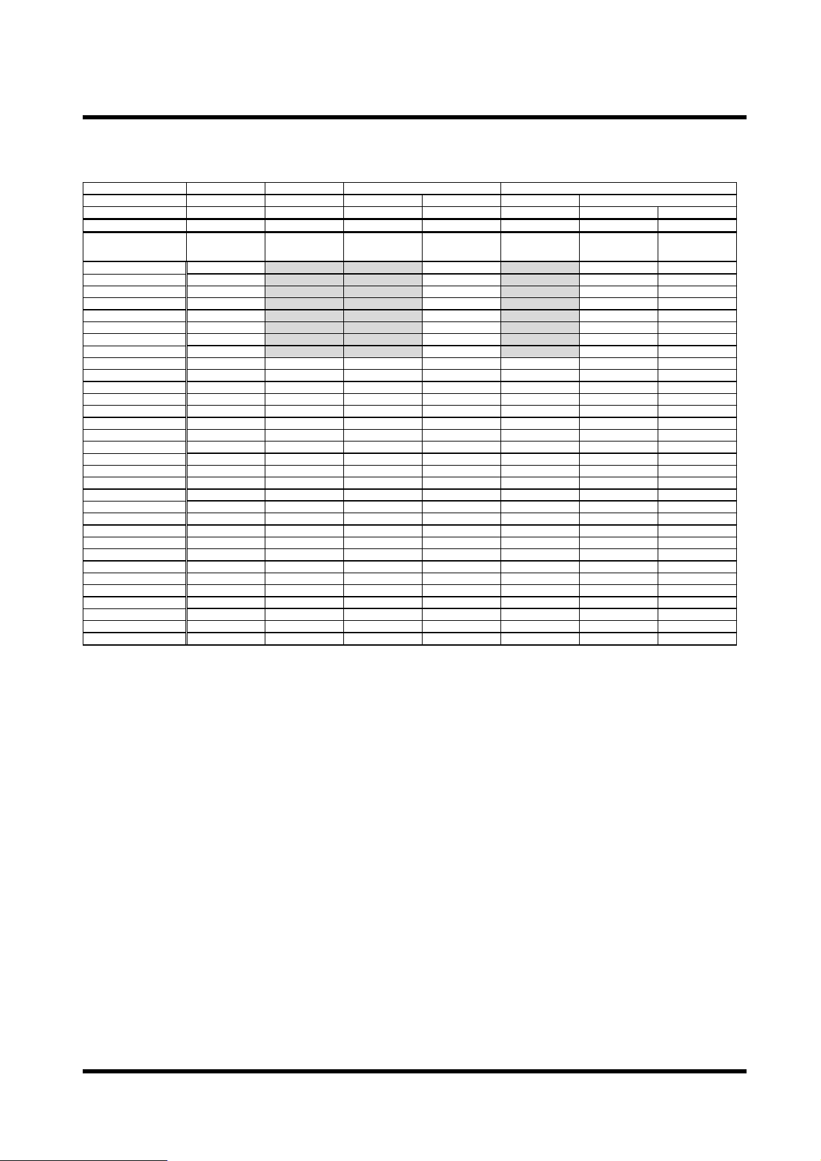
6.3 MIPI input setting
Setting of MIPI input can be configurable by 2-wire access to internal register.
Lane0 of MIPI input must always be used regardless of configuration as an obligation.
Table 1. MIPI input setting
Addr(h) Bits Register width R/W Description Default
0x1025 [0] R_RX_PN_SW 1 R/W MIPIP/Nswap 1'h0
0x1026 [7:6] R_RX_LANE_SEL0 2 R/W MIPIData Lane RX0P/RX0Npin input mapping/swap select
MIPIstandard format lane# assignment used on RX0P/RX0Ninput
The same setting as R_RX_LANE_SEL1/2/3 is prohibited. 2'h0
0x1026 [5:4] R_RX_LANE_SEL1 2 R/W MIPIData Lane RX1P/RX1Npin input mapping/swap select
MIPIstandard format lane# assignment used on RX1P/RX1Ninput
The same setting as R_RX_LANE_SEL0/2/3 is prohibited. 2'h1
0x1026 [3:2] R_RX_LANE_SEL2 2 R/W MIPIData Lane RX2P/RX2Npin input mapping/swap select
MIPIstandard format lane# assignment used on RX2P/RX2Ninput
The same setting as R_RX_LANE_SEL0/1/3 is prohibited. 2'h2
0x1026 [1:0] R_RX_LANE_SEL3 2 R/W MIPIData Lane RX3P/RX3Npin input mapping/swap select
MIPIstandard format lane# assignment used on RX3P/RX3Ninput
The same setting as R_RX_LANE_SEL0/1/2 is prohibited. 2'h3
0x102C [0] R_RX_CLKLANE_EN 1 R/W MIPIClock Lane Enable
0:Disable
1:Enable 1'h0
0x102D [4] R_RX_DATALANE_EN 1 R/W MIPIData Lane Enable
0:Disable
1:Enable, following R_RX_LANE_SEL_EN 1'h0
0x102D [1:0] R_RX_LANE_SEL_EN 2 R/W
MIPIValid Data Lane number select
00:1Lane (lane0 Enable)
01,10:2Lane (lane<1:0> Enable)
11:4Lane (lane<3:0> Enable)
2'h3

Preliminary
THCV245A_Rev.0.90_E
Copyright©2020 THine Electronics, Inc. THine Electronics, Inc.
Security C
8/67
6.4 HTPDN/LOCKN
Hot-Plug Function
HTPDN indicates Main-Link connect condition between Transmitter and Receiver. HTPDN of Transmitter side
is high when Receiver is not active or not connected. Then Transmitter can enter into power down mode. HTPDN
is set to Low by the Receiver when Receiver is active and connects to the Transmitter, and then Transmitter must
start up and transmit CDR training pattern for link training. HTPDN is open drain output at the receiver side.
Transmitter side needs Pull-up resistor.
There is an application option to omit HTPDN connection between Transmitter and Receiver. In this case,
HTPDN at Transmitter side should always be at Low.
Lock Detect Function
LOCKN indicates whether CDR PLL of Main-Link is in lock status or not. LOCKN at Transmitter input is set
to High by pull-up resistor when Receiver is not active or in CDR PLLtraining. LOCKN is set to Low byReceiver
when CDR lock is completed. After that the CDR training mode finishes and then Transmitter shifts to the normal
mode. LOCKN of Receiver is open drain. Transmitter side needs pull-up resistor.
When an application omits HTPDN, LOCKN signal should only be considered with HTPDN pulled low by
Receiver.
Vcc
(Tx side)
MSSEL
(HTPDN)
LOCKN
THCV241A
30kΩ
HTPDN
LOCKN
30kΩ
Vcc
(Tx side)
MSSEL
(HTPDN)
LOCKN
THCV241A
HTPDN
LOCKN
V-by-One®
HS Rx
30kΩ
With HTPDN connect Without HTPDN connect
V-by-One®
HS Rx
Figure 3. Physical wire connection for wired Hot-plug and Lock detect scheme
It will need same GND potential reference between transmitter and receiver device to connect HTPDN and
LOCKN pins directly like above. HTPDN and LOCKN can also be transmitted via Sub-Link without physical
wire connection. Assignment can be configurable by 2-wire access to internal register.
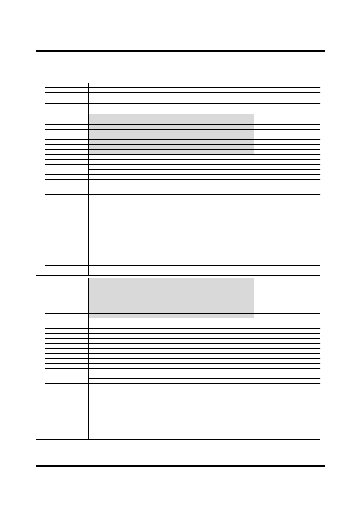
Table 2. HTPDN/LOCKN register
Addr(h) Bits Register width R/W Description Default
0x101D [1:0] R_HTPDN_SEL 2 R/W
V-by-One® HS HTPDNassignment
00:Sub-Link at PDN1=1 / HTPDNpin input at PDN1=0,
01:Reserved,
10:forced Low (Must be set at V-by-One® HS Distribution Enable),
11:forced High
2'h0
0x101E [5:4] R_LOCKN0_SEL 2 R/W V-by-One® HS LOCKNfor lane0 assignment
00:Sub-Link, 01:LOCKNpin input, 10:forced Low, 11:forced High 2'h0
0x101E [1:0] R_LOCKN1_SEL 2 R/W V-by-One® HS LOCKNfor lane1 assignment
00:Sub-Link, 01:LOCKNpin input, 10:forced Low, 11:forced High 2'h0
THCV245A
THCV245A

Preliminary
THCV245A_Rev.0.90_E
Copyright©2020 THine Electronics, Inc. THine Electronics, Inc.
Security C
9/67
6.5 V-by-One® HS output setting
Setting of V-by-One® HS output format can be configurable by 2-wire access to internal register.
Table 3. V-by-One® HS output format setting
6.5.1 MPRF (Main-Link PRivate Format)
MPRF format encoding preserves original data packet input to THCV245A and output the data packet from
counterpart V-by-One® HS receiver. The counterpart receiver must have installed MPRF format decoder like
THCV242 because MPRF is not standard format.
Output V-by-One® HS Byte Mode is 4Byte Mode.
Video formats: RAW8/10/12/14/16/20, YUV422/420, RGB888/666/565, JPEG, and User-defined generic 8-bit
are all supported with MPRF.
Figure 4. MPRF (Main-Link PRivate Format)
Addr(h) Bits Register width R/W Description Default
0x1000 [0] R_VX1_LANE 1 R/W V-by-One® HS output lane number setting
0:1lane
1:2lanes 1'h1
0x1001 [6:4] R_OUTPUT_FMT 3 R/W
V-by-One® HS output format setting
000:Main-Link PRivate Format (MPRF)
001:V-by-One® HS Standard YUV422(16bit)/RAW8
010:V-by-One® HS Standard RGB888
011:V-by-One® HS Standard RGB565
100:V-by-One® HS Standard RAW10 Mode1
101:V-by-One® HS Standard RAW12 Mode1
110: V-by-One® HS Standard RAW10 Mode2
111: V-by-One® HS Standard RAW12 Mode2
3'h0
0x1002 [5] R_HFSEL 1 R/W V-by-One® HS HFSEL (High Freq. SELect) mode Enable
0:HFMode Disable
1:HFMode Enable 1'h0
0x1055 [1:0] R_BITMAP_SEL 2 R/W V-by-One® HS output data mapping select
00:MAP1, 01:MAP2, 10:MAP3, 11:MAP4 2'h0
THCV245ACMOS Sensor THCV242 Processor
In ECU or
controller
Original
Data packet
(format,
payload, etc.)
Preserved
Data packet
(format,
payload, etc.)
Main-Link
MPRF
format

Preliminary
THCV245A_Rev.0.90_E
Copyright©2020 THine Electronics, Inc. THine Electronics, Inc.
Security C
10/67
6.5.2 V-by-One® HS standard format
THCV245A output format capabilities as transmitter are shown as follows. D[31:0] indicates V-by-One®HS
standard version1.5 Packer packet definition. Data can be transmitted normally only when both transmitter and
receiver are set to the same available format. Some of the THCV245A format may not be supported by particular
counterpart receiver because THCV245A prepares multiple formats that suit to multiple receiver devices
alternatives.
Table 4. V-by-One® HS 1lane output data mapping format 1/3
R_OUTPUT_FMT 1
R_HFSEL 0 1
R_BITMAP_SEL 0 1 2 0 3 0 1
default V-by-One®HS Byte Mode 3333344
Format Name
Vx1HS std. Packer Packet ref. YUV422
Map1 YUV422
Map2 YUV422
Map3 RAW8 RAW8
Map4 YUV422HF
Map1 YUV422HF
Map2
V-by-One®HS_D[31] - - - - - Y[7](1st) Cb(U)[7]
V-by-One®HS_D[30] - - - - - Y[6](1st) Cb(U)[6]
V-by-One®HS_D[29] - - - - - Y[5](1st) Cb(U)[5]
V-by-One®HS_D[28] - - - - - Y[4](1st) Cb(U)[4]
V-by-One®HS_D[27] - - - - - Y[3](1st) Cb(U)[3]
V-by-One®HS_D[26] - - - - - Y[2](1st) Cb(U)[2]
V-by-One®HS_D[25] - - - - - Y[1](1st) Cb(U)[1]
V-by-One®HS_D[24] - - - - - Y[0](1st) Cb(U)[0]
V-by-One®HS_D[23] Cb(U)[7]/Cr(V)[7] Y[7](1st)/Y[7](2nd) 0 RAW[7] (1st) RAW[7] (1st) Cb(U)[7] Y[7](1st)
V-by-One®HS_D[22] Cb(U)[6]/Cr(V)[6] Y[6](1st)/Y[6](2nd) 0 RAW[6] (1st) RAW[6] (1st) Cb(U)[6] Y[6](1st)
V-by-One®HS_D[21] Cb(U)[5]/Cr(V)[5] Y[5](1st)/Y[5](2nd) 0 RAW[5] (1st) RAW[5] (1st) Cb(U)[5] Y[5](1st)
V-by-One®HS_D[20] Cb(U)[4]/Cr(V)[4] Y[4](1st)/Y[4](2nd) 0 RAW[4] (1st) RAW[4] (1st) Cb(U)[4] Y[4](1st)
V-by-One®HS_D[19] Cb(U)[3]/Cr(V)[3] Y[3](1st)/Y[3](2nd) 0 RAW[3] (1st) RAW[3] (1st) Cb(U)[3] Y[3](1st)
V-by-One®HS_D[18] Cb(U)[2]/Cr(V)[2] Y[2](1st)/Y[2](2nd) 0 RAW[2] (1st) RAW[2] (1st) Cb(U)[2] Y[2](1st)
V-by-One®HS_D[17] Cb(U)[1]/Cr(V)[1] Y[1](1st)/Y[1](2nd) 0 RAW[1] (1st) RAW[1] (1st) Cb(U)[1] Y[1](1st)
V-by-One®HS_D[16] Cb(U)[0]/Cr(V)[0] Y[0](1st)/Y[0](2nd) 0 RAW[0] (1st) RAW[0] (1st) Cb(U)[0] Y[0](1st)
V-by-One®HS_D[15] 0 0 Y[7](1st)/Y[7](2nd) 0 0 Y[7](2nd) Cr(V)[7]
V-by-One®HS_D[14] 0 0 Y[6](1st)/Y[6](2nd) 0 0 Y[6](2nd) Cr(V)[6]
V-by-One®HS_D[13] 0 0 Y[5](1st)/Y[5](2nd) 0 0 Y[5(2nd) Cr(V)[5]
V-by-One®HS_D[12] 0 0 Y[4](1st)/Y[4](2nd) 0 0 Y[4](2nd) Cr(V)[4]
V-by-One®HS_D[11] 0 0 Y[3](1st)/Y[3](2nd) 0 RAW[7] (2nd) Y[3](2nd) Cr(V)[3]
V-by-One®HS_D[10] 0 0 Y[2](1st)/Y[2](2nd) 0 RAW[6] (2nd) Y[2](2nd) Cr(V)[2]
V-by-One®HS_D[9] 0 0 Y[1](1st)/Y[1](2nd) 0 RAW[5] (2nd) Y[1](2nd) Cr(V)[1]
V-by-One®HS_D[8] 0 0 Y[0](1st)/Y[0](2nd) 0 RAW[4] (2nd) Y[0](2nd) Cr(V)[0]
V-by-One®HS_D[7] Y[7](1st)/Y[7](2nd) Cb(U)[7]/Cr(V)[7] Cb(U)[7]/Cr(V)[7] RAW[7] (2nd) RAW[3] (2nd) Cr(V)[7] Y[7](2nd)
V-by-One®HS_D[6] Y[6](1st)/Y[6](2nd) Cb(U)[6]/Cr(V)[6] Cb(U)[6]/Cr(V)[6] RAW[6] (2nd) RAW[2] (2nd) Cr(V)[6] Y[6](2nd)
V-by-One®HS_D[5] Y[5](1st)/Y[5](2nd) Cb(U)[5]/Cr(V)[5] Cb(U)[5]/Cr(V)[5] RAW[5] (2nd) RAW[1] (2nd) Cr(V)[5] Y[5(2nd)
V-by-One®HS_D[4] Y[4](1st)/Y[4](2nd) Cb(U)[4]/Cr(V)[4] Cb(U)[4]/Cr(V)[4] RAW[4] (2nd) RAW[0] (2nd) Cr(V)[4] Y[4](2nd)
V-by-One®HS_D[3] Y[3](1st)/Y[3](2nd) Cb(U)[3]/Cr(V)[3] Cb(U)[3]/Cr(V)[3] RAW[3] (2nd) 0 Cr(V)[3] Y[3](2nd)
V-by-One®HS_D[2] Y[2](1st)/Y[2](2nd) Cb(U)[2]/Cr(V)[2] Cb(U)[2]/Cr(V)[2] RAW[2] (2nd) 0 Cr(V)[2] Y[2](2nd)
V-by-One®HS_D[1] Y[1](1st)/Y[1](2nd) Cb(U)[1]/Cr(V)[1] Cb(U)[1]/Cr(V)[1] RAW[1] (2nd) 0 Cr(V)[1] Y[1](2nd)
V-by-One®HS_D[0] Y[0](1st)/Y[0](2nd) Cb(U)[0]/Cr(V)[0] Cb(U)[0]/Cr(V)[0] RAW[0] (2nd) 0 Cr(V)[0] Y[0](2nd)
Preliminary
THCV245A_Rev.0.90_E
Copyright©2020 THine Electronics, Inc. THine Electronics, Inc.
Security C
11/67
Table 5. V-by-One® HS 1lane output data mapping format 2/3
R_OUTPUT_FMT 1 2 3 4
R_HFSEL 1 - 0 1 0 1 1
R_BITMAP_SEL 2 - 0 0 0 0 2
default V-by-One®HS Byte Mode 4334344
Format Name
Vx1HS std. Packer Packet ref. RAW8HF RGB888 RGB565 RGB565HF RAW10 RAW10HF
Map1 RAW10HF
Map3
V-by-One®HS_D[31] RAW[7] (2nd) - - B[4] (1st) - 0 0
V-by-One®HS_D[30] RAW[6] (2nd) - - B[3] (1st) - 0 0
V-by-One®HS_D[29] RAW[5] (2nd) - - B[2] (1st) - 0 0
V-by-One®HS_D[28] RAW[4] (2nd) - - B[1] (1st) - 0 0
V-by-One®HS_D[27] RAW[3] (2nd) - - B[0] (1st) - 0 RAW[9] (1st)
V-by-One®HS_D[26] RAW[2] (2nd) - - G[5] (1st) - 0 RAW[8] (1st)
V-by-One®HS_D[25] RAW[1] (2nd) - - G[4] (1st) - RAW[1] (1st) RAW[7] (1st)
V-by-One®HS_D[24] RAW[0] (2nd) - - G[3] (1st) - RAW[0] (1st) RAW[6] (1st)
V-by-One®HS_D[23] RAW[7] (1st) B[7] B[4] G[2] (1st) 0 RAW[9] (1st) RAW[5] (1st)
V-by-One®HS_D[22] RAW[6] (1st) B[6] B[3] G[1] (1st) 0 RAW[8] (1st) RAW[4] (1st)
V-by-One®HS_D[21] RAW[5] (1st) B[5] B[2] G[0] (1st) 0 RAW[7] (1st) RAW[3] (1st)
V-by-One®HS_D[20] RAW[4] (1st) B[4] B[1] R[4] (1st) 0 RAW[6] (1st) RAW[2] (1st)
V-by-One®HS_D[19] RAW[3] (1st) B[3] B[0] R[3] (1st) 0 RAW[5] (1st) RAW[1] (1st)
V-by-One®HS_D[18] RAW[2] (1st) B[2] 0 R[2] (1st) 0 RAW[4] (1st) RAW[0] (1st)
V-by-One®HS_D[17] RAW[1] (1st) B[1] 0 R[1] (1st) 0 RAW[3] (1st) 0
V-by-One®HS_D[16] RAW[0] (1st) B[0] 0 R[0] (1st) 0 RAW[2] (1st) 0
V-by-One®HS_D[15] RAW[7] (4th) G[7] G[5] B[4] (2nd) 0 0 0
V-by-One®HS_D[14] RAW[6] (4th) G[6] G[4] B[3] (2nd) 0 0 0
V-by-One®HS_D[13] RAW[5] (4th) G[5] G[3] B[2] (2nd) 0 0 0
V-by-One®HS_D[12] RAW[4] (4th) G[4] G[2] B[1] (2nd) 0 0 0
V-by-One®HS_D[11] RAW[3] (4th) G[3] G[1] B[0] (2nd) 0 0 RAW[9] (2nd)
V-by-One®HS_D[10] RAW[2] (4th) G[2] G[0] G[5] (2nd) 0 0 RAW[8] (2nd)
V-by-One®HS_D[9] RAW[1] (4th) G[1] 0 G[4] (2nd) RAW[1] RAW[1] (2nd) RAW[7] (2nd)
V-by-One®HS_D[8] RAW[0] (4th) G[0] 0 G[3] (2nd) RAW[0] RAW[0] (2nd) RAW[6] (2nd)
V-by-One®HS_D[7] RAW[7] (3rd) R[7] R[4] G[2] (2nd) RAW[9] RAW[9] (2nd) RAW[5] (2nd)
V-by-One®HS_D[6] RAW[6] (3rd) R[6] R[3] G[1] (2nd) RAW[8] RAW[8] (2nd) RAW[4] (2nd)
V-by-One®HS_D[5] RAW[5] (3rd) R[5] R[2] G[0] (2nd) RAW[7] RAW[7] (2nd) RAW[3] (2nd)
V-by-One®HS_D[4] RAW[4] (3rd) R[4] R[1] R[4] (2nd) RAW[6] RAW[6] (2nd) RAW[2] (2nd)
V-by-One®HS_D[3] RAW[3] (3rd) R[3] R[0] R[3] (2nd) RAW[5] RAW[5] (2nd) RAW[1] (2nd)
V-by-One®HS_D[2] RAW[2] (3rd) R[2] 0 R[2] (2nd) RAW[4] RAW[4] (2nd) RAW[0] (2nd)
V-by-One®HS_D[1] RAW[1] (3rd) R[1] 0 R[1] (2nd) RAW[3] RAW[3] (2nd) 0
V-by-One®HS_D[0] RAW[0] (3rd) R[0] 0 R[0] (2nd) RAW[2] RAW[2] (2nd) 0

Preliminary
THCV245A_Rev.0.90_E
Copyright©2020 THine Electronics, Inc. THine Electronics, Inc.
Security C
12/67
Table 6. V-by-One® HS 1lane output data mapping format 3/3
R_OUTPUT_FMT 5 6 7
R_HFSEL 0 1 1 - - - -
R_BITMAP_SEL 0 0 1 0 2 0 1
default V-by-One®HS Byte Mode 3 4 4 3 3 3 3
Format Name
Vx1HS std. Packer Packet ref. RAW12 RAW12HF
Map1 RAW12HF
Map2 RAW10HF2
Map1 RAW10HF2
Map3 RAW12HF2
Map1 RAW12HF2
Map2
V-by-One®HS_D[31] - 0 0 - - - -
V-by-One®HS_D[30] - 0 0 - - - -
V-by-One®HS_D[29] - 0 0 - - - -
V-by-One®HS_D[28] - 0 0 - - - -
V-by-One®HS_D[27] - RAW[3] (1st) RAW[11] (1st) - - - -
V-by-One®HS_D[26] - RAW[2] (1st) RAW[10] (1st) - - - -
V-by-One®HS_D[25] - RAW[1] (1st) RAW[9] (1st) - - - -
V-by-One®HS_D[24] - RAW[0] (1st) RAW[8] (1st) - - - -
V-by-One®HS_D[23] 0 RAW[11] (1st) RAW[7] (1st) 0 RAW[9] (1st) RAW[3] (1st) RAW[11] (1st)
V-by-One®HS_D[22] 0 RAW[10] (1st) RAW[6] (1st) 0 RAW[8] (1st) RAW[2] (1st) RAW[10] (1st)
V-by-One®HS_D[21] 0 RAW[9] (1st) RAW[5] (1st) RAW[1] (1st) RAW[7] (1st) RAW[1] (1st) RAW[9] (1st)
V-by-One®HS_D[20] 0 RAW[8] (1st) RAW[4] (1st) RAW[0] (1st) RAW[6] (1st) RAW[0] (1st) RAW[8] (1st)
V-by-One®HS_D[19] 0 RAW[7] (1st) RAW[3] (1st) RAW[9] (1st) RAW[5] (1st) RAW[11] (1st) RAW[7] (1st)
V-by-One®HS_D[18] 0 RAW[6] (1st) RAW[2] (1st) RAW[8] (1st) RAW[4] (1st) RAW[10] (1st) RAW[6] (1st)
V-by-One®HS_D[17] 0 RAW[5] (1st) RAW[1] (1st) RAW[7] (1st) RAW[3] (1st) RAW[9] (1st) RAW[5] (1st)
V-by-One®HS_D[16] 0 RAW[4] (1st) RAW[0] (1st) RAW[6] (1st) RAW[2] (1st) RAW[8] (1st) RAW[4] (1st)
V-by-One®HS_D[15] 0 0 0 RAW[5] (1st) RAW[1] (1st) RAW[7] (1st) RAW[3] (1st)
V-by-One®HS_D[14] 0 0 0 RAW[4] (1st) RAW[0] (1st) RAW[6] (1st) RAW[2] (1st)
V-by-One®HS_D[13] 0 0 0 RAW[3] (1st) 0 RAW[5] (1st) RAW[1] (1st)
V-by-One®HS_D[12] 0 0 0 RAW[2] (1st) 0 RAW[4] (1st) RAW[0] (1st)
V-by-One®HS_D[11] RAW[3] RAW[3] (2nd) RAW[11] (2nd) 0 RAW[9] (2nd) RAW[3] (2nd) RAW[11] (2nd)
V-by-One®HS_D[10] RAW[2] RAW[2] (2nd) RAW[10] (2nd) 0 RAW[8] (2nd) RAW[2] (2nd) RAW[10] (2nd)
V-by-One®HS_D[9] RAW[1] RAW[1] (2nd) RAW[9] (2nd) RAW[1] (2nd) RAW[7] (2nd) RAW[1] (2nd) RAW[9] (2nd)
V-by-One®HS_D[8] RAW[0] RAW[0] (2nd) RAW[8] (2nd) RAW[0] (2nd) RAW[6] (2nd) RAW[0] (2nd) RAW[8] (2nd)
V-by-One®HS_D[7] RAW[11] RAW[11] (2nd) RAW[7] (2nd) RAW[9] (2nd) RAW[5] (2nd) RAW[11] (2nd) RAW[7] (2nd)
V-by-One®HS_D[6] RAW[10] RAW[10] (2nd) RAW[6] (2nd) RAW[8] (2nd) RAW[4] (2nd) RAW[10] (2nd) RAW[6] (2nd)
V-by-One®HS_D[5] RAW[9] RAW[9] (2nd) RAW[5] (2nd) RAW[7] (2nd) RAW[3] (2nd) RAW[9] (2nd) RAW[5] (2nd)
V-by-One®HS_D[4] RAW[8] RAW[8] (2nd) RAW[4] (2nd) RAW[6] (2nd) RAW[2] (2nd) RAW[8] (2nd) RAW[4] (2nd)
V-by-One®HS_D[3] RAW[7] RAW[7] (2nd) RAW[3] (2nd) RAW[5] (2nd) RAW[1] (2nd) RAW[7] (2nd) RAW[3] (2nd)
V-by-One®HS_D[2] RAW[6] RAW[6] (2nd) RAW[2] (2nd) RAW[4] (2nd) RAW[0] (2nd) RAW[6] (2nd) RAW[2] (2nd)
V-by-One®HS_D[1] RAW[5] RAW[5] (2nd) RAW[1] (2nd) RAW[3] (2nd) 0 RAW[5] (2nd) RAW[1] (2nd)
V-by-One®HS_D[0] RAW[4] RAW[4] (2nd) RAW[0] (2nd) RAW[2] (2nd) 0 RAW[4] (2nd) RAW[0] (2nd)
Preliminary
THCV245A_Rev.0.90_E
Copyright©2020 THine Electronics, Inc. THine Electronics, Inc.
Security C
13/67
Table 7. V-by-One® HS 2lane output data mapping format 1/3
R_OUTPUT_FMT 1
R_HFSEL 0 1
R_BITMAP_SEL 0 1 2 0 3 0 1
default V-by-One®HS Byte Mode 3 3 3 3 3 4 4
Format Name YUV422
Map1 YUV422
Map2 YUV422
Map3 RAW8 RAW8
Map4 YUV422HF
Map1 YUV422HF
Map2
V-by-One®HS_D[31] - - - - - Y[7](1st) Cb(U)[7](1st)
V-by-One®HS_D[30] - - - - - Y[6](1st) Cb(U)[6](1st)
V-by-One®HS_D[29] - - - - - Y[5](1st) Cb(U)[5](1st)
V-by-One®HS_D[28] - - - - - Y[4](1st) Cb(U)[4](1st)
V-by-One®HS_D[27] - - - - - Y[3](1st) Cb(U)[3](1st)
V-by-One®HS_D[26] - - - - - Y[2](1st) Cb(U)[2](1st)
V-by-One®HS_D[25] - - - - - Y[1](1st) Cb(U)[1](1st)
V-by-One®HS_D[24] - - - - - Y[0](1st) Cb(U)[0](1st)
V-by-One®HS_D[23] Cb(U)[7] Cr(V)[7] 0 RAW[7] (1st) RAW[7] (1st) Cb(U)[7](1st) Y[7](1st)
V-by-One®HS_D[22] Cb(U)[6] Cr(V)[6] 0 RAW[6] (1st) RAW[6] (1st) Cb(U)[6](1st) Y[6](1st)
V-by-One®HS_D[21] Cb(U)[5] Cr(V)[5] 0 RAW[5] (1st) RAW[5] (1st) Cb(U)[5](1st) Y[5](1st)
V-by-One®HS_D[20] Cb(U)[4] Cr(V)[4] 0 RAW[4] (1st) RAW[4] (1st) Cb(U)[4](1st) Y[4](1st)
V-by-One®HS_D[19] Cb(U)[3] Cr(V)[3] 0 RAW[3] (1st) RAW[3] (1st) Cb(U)[3](1st) Y[3](1st)
V-by-One®HS_D[18] Cb(U)[2] Cr(V)[2] 0 RAW[2] (1st) RAW[2] (1st) Cb(U)[2](1st) Y[2](1st)
V-by-One®HS_D[17] Cb(U)[1] Cr(V)[1] 0 RAW[1] (1st) RAW[1] (1st) Cb(U)[1](1st) Y[1](1st)
V-by-One®HS_D[16] Cb(U)[0] Cr(V)[0] 0 RAW[0] (1st) RAW[0] (1st) Cb(U)[0](1st) Y[0](1st)
V-by-One®HS_D[15] 0 0 Y[7](1st) 0 0 Y[7] (3rd) Cb(U)[7] (3rd)
V-by-One®HS_D[14] 0 0 Y[6](1st) 0 0 Y[6] (3rd) Cb(U)[6] (3rd)
V-by-One®HS_D[13] 0 0 Y[5](1st) 0 0 Y[5] (3rd) Cb(U)[5] (3rd)
V-by-One®HS_D[12] 0 0 Y[4](1st) 0 0 Y[4] (3rd) Cb(U)[4] (3rd)
V-by-One®HS_D[11] 0 0 Y[3](1st) 0 RAW[7] (3rd) Y[3] (3rd) Cb(U)[3] (3rd)
V-by-One®HS_D[10] 0 0 Y[2](1st) 0 RAW[6] (3rd) Y[2] (3rd) Cb(U)[2] (3rd)
V-by-One®HS_D[9] 0 0 Y[1](1st) 0 RAW[5] (3rd) Y[1] (3rd) Cb(U)[1] (3rd)
V-by-One®HS_D[8] 0 0 Y[0](1st) 0 RAW[4] (3rd) Y[0] (3rd) Cb(U)[0] (3rd)
V-by-One®HS_D[7] Cr(V)[7] Cb(U)[7] Cb(U)[7] RAW[7] (3rd) RAW[3] (3rd) Cb(U)[7] (3rd) Y[7] (3rd)
V-by-One®HS_D[6] Cr(V)[6] Cb(U)[6] Cb(U)[6] RAW[6] (3rd) RAW[2] (3rd) Cb(U)[6] (3rd) Y[6] (3rd)
V-by-One®HS_D[5] Cr(V)[5] Cb(U)[5] Cb(U)[5] RAW[5] (3rd) RAW[1] (3rd) Cb(U)[5] (3rd) Y[5] (3rd)
V-by-One®HS_D[4] Cr(V)[4] Cb(U)[4] Cb(U)[4] RAW[4] (3rd) RAW[0] (3rd) Cb(U)[4] (3rd) Y[4] (3rd)
V-by-One®HS_D[3] Cr(V)[3] Cb(U)[3] Cb(U)[3] RAW[3] (3rd) 0 Cb(U)[3] (3rd) Y[3] (3rd)
V-by-One®HS_D[2] Cr(V)[2] Cb(U)[2] Cb(U)[2] RAW[2] (3rd) 0 Cb(U)[2] (3rd) Y[2] (3rd)
V-by-One®HS_D[1] Cr(V)[1] Cb(U)[1] Cb(U)[1] RAW[1] (3rd) 0 Cb(U)[1] (3rd) Y[1] (3rd)
V-by-One®HS_D[0] Cr(V)[0] Cb(U)[0] Cb(U)[0] RAW[0] (3rd) 0 Cb(U)[0] (3rd) Y[0] (3rd)
V-by-One®HS_D[31] - - - - - Y[7] (2nd) Cr(V)[7] (2nd)
V-by-One®HS_D[30] - - - - - Y[6] (2nd) Cr(V)[6] (2nd)
V-by-One®HS_D[29] - - - - - Y[5] (2nd) Cr(V)[5] (2nd)
V-by-One®HS_D[28] - - - - - Y[4] (2nd) Cr(V)[4] (2nd)
V-by-One®HS_D[27] - - - - - Y[3] (2nd) Cr(V)[3] (2nd)
V-by-One®HS_D[26] - - - - - Y[2] (2nd) Cr(V)[2] (2nd)
V-by-One®HS_D[25] - - - - - Y[1] (2nd) Cr(V)[1] (2nd)
V-by-One®HS_D[24] - - - - - Y[0] (2nd) Cr(V)[0] (2nd)
V-by-One®HS_D[23] Y[7] (1st) Y[7](2nd) 0 RAW[7] (2nd) RAW[7] (2nd) Cr(V)[7] (2nd) Y[7] (2nd)
V-by-One®HS_D[22] Y[6] (1st) Y[6](2nd) 0 RAW[6] (2nd) RAW[6] (2nd) Cr(V)[6] (2nd) Y[6] (2nd)
V-by-One®HS_D[21] Y[5] (1st) Y[5](2nd) 0 RAW[5] (2nd) RAW[5] (2nd) Cr(V)[5] (2nd) Y[5] (2nd)
V-by-One®HS_D[20] Y[4] (1st) Y[4](2nd) 0 RAW[4] (2nd) RAW[4] (2nd) Cr(V)[4] (2nd) Y[4] (2nd)
V-by-One®HS_D[19] Y[3] (1st) Y[3](2nd) 0 RAW[3] (2nd) RAW[3] (2nd) Cr(V)[3] (2nd) Y[3] (2nd)
V-by-One®HS_D[18] Y[2] (1st) Y[2](2nd) 0 RAW[2] (2nd) RAW[2] (2nd) Cr(V)[2] (2nd) Y[2] (2nd)
V-by-One®HS_D[17] Y[1] (1st) Y[1](2nd) 0 RAW[1] (2nd) RAW[1] (2nd) Cr(V)[1] (2nd) Y[1] (2nd)
V-by-One®HS_D[16] Y[0] (1st) Y[0](2nd) 0 RAW[0] (2nd) RAW[0] (2nd) Cr(V)[0] (2nd) Y[0] (2nd)
V-by-One®HS_D[15] 0 0 Y[7](2nd) 0 0 Y[7] (4th) Cr(V)[7] (4th)
V-by-One®HS_D[14] 0 0 Y[6](2nd) 0 0 Y[6] (4th) Cr(V)[6] (4th)
V-by-One®HS_D[13] 0 0 Y[5](2nd) 0 0 Y[5] (4th) Cr(V)[5] (4th)
V-by-One®HS_D[12] 0 0 Y[4](2nd) 0 0 Y[4] (4th) Cr(V)[4] (4th)
V-by-One®HS_D[11] 0 0 Y[3](2nd) 0 RAW[7] (4th) Y[3] (4th) Cr(V)[3] (4th)
V-by-One®HS_D[10] 0 0 Y[2](2nd) 0 RAW[6] (4th) Y[2] (4th) Cr(V)[2] (4th)
V-by-One®HS_D[9] 0 0 Y[1](2nd) 0 RAW[5] (4th) Y[1] (4th) Cr(V)[1] (4th)
V-by-One®HS_D[8] 0 0 Y[0](2nd) 0 RAW[4] (4th) Y[0] (4th) Cr(V)[0] (4th)
V-by-One®HS_D[7] Y[7] (2nd) Y[7](1st) Cr(V)[7] RAW[7] (4th) RAW[3] (4th) Cr(V)[7] (4th) Y[7] (4th)
V-by-One®HS_D[6] Y[6] (2nd) Y[6](1st) Cr(V)[6] RAW[6] (4th) RAW[2] (4th) Cr(V)[6] (4th) Y[6] (4th)
V-by-One®HS_D[5] Y[5] (2nd) Y[5](1st) Cr(V)[5] RAW[5] (4th) RAW[1] (4th) Cr(V)[5] (4th) Y[5] (4th)
V-by-One®HS_D[4] Y[4] (2nd) Y[4](1st) Cr(V)[4] RAW[4] (4th) RAW[0] (4th) Cr(V)[4] (4th) Y[4] (4th)
V-by-One®HS_D[3] Y[3] (2nd) Y[3](1st) Cr(V)[3] RAW[3] (4th) 0 Cr(V)[3] (4th) Y[3] (4th)
V-by-One®HS_D[2] Y[2] (2nd) Y[2](1st) Cr(V)[2] RAW[2] (4th) 0 Cr(V)[2] (4th) Y[2] (4th)
V-by-One®HS_D[1] Y[1] (2nd) Y[1](1st) Cr(V)[1] RAW[1] (4th) 0 Cr(V)[1] (4th) Y[1] (4th)
V-by-One®HS_D[0] Y[0] (2nd) Y[0](1st) Cr(V)[0] RAW[0] (4th) 0 Cr(V)[0] (4th) Y[0] (4th)
TX0P/N V-by-One® HS lane0TX1P/N V-by-One® HS lane1
Preliminary
THCV245A_Rev.0.90_E
Copyright©2020 THine Electronics, Inc. THine Electronics, Inc.
Security C
14/67
Table 8. V-by-One® HS 2lane output data mapping format 2/3
R_OUTPUT_FMT 1 2 3 4
R_HFSEL 1 - 0 1 0 1
R_BITMAP_SEL 2 - 0 0 0 0 2
default V-by-One®HS Byte Mode 4 3 3 4 3 4 4
Format Name RAW8HF RGB888 RGB565 RGB565HF RAW10 RAW10HF
Map1 RAW10HF
Map3
V-by-One®HS_D[31] RAW[7] (2nd) - - B[4] (1st) - 0 0
V-by-One®HS_D[30] RAW[6] (2nd) - - B[3] (1st) - 0 0
V-by-One®HS_D[29] RAW[5] (2nd) - - B[2] (1st) - 0 0
V-by-One®HS_D[28] RAW[4] (2nd) - - B[1] (1st) - 0 0
V-by-One®HS_D[27] RAW[3] (2nd) - - B[0] (1st) - 0 RAW[9] (1st)
V-by-One®HS_D[26] RAW[2] (2nd) - - G[5] (1st) - 0 RAW[8] (1st)
V-by-One®HS_D[25] RAW[1] (2nd) - - G[4] (1st) - RAW[1] (1st) RAW[7] (1st)
V-by-One®HS_D[24] RAW[0] (2nd) - - G[3] (1st) - RAW[0] (1st) RAW[6] (1st)
V-by-One®HS_D[23] RAW[7] (1st) B[7] (1st) B[4] (1st) G[2] (1st) 0 RAW[9] (1st) RAW[5] (1st)
V-by-One®HS_D[22] RAW[6] (1st) B[6] (1st) B[3] (1st) G[1] (1st) 0 RAW[8] (1st) RAW[4] (1st)
V-by-One®HS_D[21] RAW[5] (1st) B[5] (1st) B[2] (1st) G[0] (1st) 0 RAW[7] (1st) RAW[3] (1st)
V-by-One®HS_D[20] RAW[4] (1st) B[4] (1st) B[1] (1st) R[4] (1st) 0 RAW[6] (1st) RAW[2] (1st)
V-by-One®HS_D[19] RAW[3] (1st) B[3] (1st) B[0] (1st) R[3] (1st) 0 RAW[5] (1st) RAW[1] (1st)
V-by-One®HS_D[18] RAW[2] (1st) B[2] (1st) 0 R[2] (1st) 0 RAW[4] (1st) RAW[0] (1st)
V-by-One®HS_D[17] RAW[1] (1st) B[1] (1st) 0 R[1] (1st) 0 RAW[3] (1st) 0
V-by-One®HS_D[16] RAW[0] (1st) B[0] (1st) 0 R[0] (1st) 0 RAW[2] (1st) 0
V-by-One®HS_D[15] RAW[7] (6th) G[7] (1st) G[5] (1st) B[4] (3rd) 0 0 0
V-by-One®HS_D[14] RAW[6] (6th) G[6] (1st) G[4] (1st) B[3] (3rd) 0 0 0
V-by-One®HS_D[13] RAW[5] (6th) G[5] (1st) G[3] (1st) B[2] (3rd) 0 0 0
V-by-One®HS_D[12] RAW[4] (6th) G[4] (1st) G[2] (1st) B[1] (3rd) 0 0 0
V-by-One®HS_D[11] RAW[3] (6th) G[3] (1st) G[1] (1st) B[0] (3rd) 0 0 RAW[9] (3rd)
V-by-One®HS_D[10] RAW[2] (6th) G[2] (1st) G[0] (1st) G[5] (3rd) 0 0 RAW[8] (3rd)
V-by-One®HS_D[9] RAW[1] (6th) G[1] (1st) 0 G[4] (3rd) RAW[1] (1st) RAW[1] (3rd) RAW[7] (3rd)
V-by-One®HS_D[8] RAW[0] (6th) G[0] (1st) 0 G[3] (3rd) RAW[0] (1st) RAW[0] (3rd) RAW[6] (3rd)
V-by-One®HS_D[7] RAW[7] (5th) R[7] (1st) R[4] (1st) G[2] (3rd) RAW[9] (1st) RAW[9] (3rd) RAW[5] (3rd)
V-by-One®HS_D[6] RAW[6] (5th) R[6] (1st) R[3] (1st) G[1] (3rd) RAW[8] (1st) RAW[8] (3rd) RAW[4] (3rd)
V-by-One®HS_D[5] RAW[5] (5th) R[5] (1st) R[2] (1st) G[0] (3rd) RAW[7] (1st) RAW[7] (3rd) RAW[3] (3rd)
V-by-One®HS_D[4] RAW[4] (5th) R[4] (1st) R[1] (1st) R[4] (3rd) RAW[6] (1st) RAW[6] (3rd) RAW[2] (3rd)
V-by-One®HS_D[3] RAW[3] (5th) R[3] (1st) R[0] (1st) R[3] (3rd) RAW[5] (1st) RAW[5] (3rd) RAW[1] (3rd)
V-by-One®HS_D[2] RAW[2] (5th) R[2] (1st) 0 R[2] (3rd) RAW[4] (1st) RAW[4] (3rd) RAW[0] (3rd)
V-by-One®HS_D[1] RAW[1] (5th) R[1] (1st) 0 R[1] (3rd) RAW[3] (1st) RAW[3] (3rd) 0
V-by-One®HS_D[0] RAW[0] (5th) R[0] (1st) 0 R[0] (3rd) RAW[2] (1st) RAW[2] (3rd) 0
V-by-One®HS_D[31] RAW[7] (4th) - - B[4] (2nd) - 0 0
V-by-One®HS_D[30] RAW[6] (4th) - - B[3] (2nd) - 0 0
V-by-One®HS_D[29] RAW[5] (4th) - - B[2] (2nd) - 0 0
V-by-One®HS_D[28] RAW[4] (4th) - - B[1] (2nd) - 0 0
V-by-One®HS_D[27] RAW[3] (4th) - - B[0] (2nd) - 0 RAW[9] (2nd)
V-by-One®HS_D[26] RAW[2] (4th) - - G[5] (2nd) - 0 RAW[8] (2nd)
V-by-One®HS_D[25] RAW[1] (4th) - - G[4] (2nd) - RAW[1] (2nd) RAW[7] (2nd)
V-by-One®HS_D[24] RAW[0] (4th) - - G[3] (2nd) - RAW[0] (2nd) RAW[6] (2nd)
V-by-One®HS_D[23] RAW[7] (3rd) B[7] (2nd) B[4] (2nd) G[2] (2nd) 0 RAW[9] (2nd) RAW[5] (2nd)
V-by-One®HS_D[22] RAW[6] (3rd) B[6] (2nd) B[3] (2nd) G[1] (2nd) 0 RAW[8] (2nd) RAW[4] (2nd)
V-by-One®HS_D[21] RAW[5] (3rd) B[5] (2nd) B[2] (2nd) G[0] (2nd) 0 RAW[7] (2nd) RAW[3] (2nd)
V-by-One®HS_D[20] RAW[4] (3rd) B[4] (2nd) B[1] (2nd) R[4] (2nd) 0 RAW[6] (2nd) RAW[2] (2nd)
V-by-One®HS_D[19] RAW[3] (3rd) B[3] (2nd) B[0] (2nd) R[3] (2nd) 0 RAW[5] (2nd) RAW[1] (2nd)
V-by-One®HS_D[18] RAW[2] (3rd) B[2] (2nd) 0 R[2] (2nd) 0 RAW[4] (2nd) RAW[0] (2nd)
V-by-One®HS_D[17] RAW[1] (3rd) B[1] (2nd) 0 R[1] (2nd) 0 RAW[3] (2nd) 0
V-by-One®HS_D[16] RAW[0] (3rd) B[0] (2nd) 0 R[0] (2nd) 0 RAW[2] (2nd) 0
V-by-One®HS_D[15] RAW[7] (8th) G[7] (2nd) G[5] (2nd) B[4] (4th) 0 0 0
V-by-One®HS_D[14] RAW[6] (8th) G[6] (2nd) G[4] (2nd) B[3] (4th) 0 0 0
V-by-One®HS_D[13] RAW[5] (8th) G[5] (2nd) G[3] (2nd) B[2] (4th) 0 0 0
V-by-One®HS_D[12] RAW[4] (8th) G[4] (2nd) G[2] (2nd) B[1] (4th) 0 0 0
V-by-One®HS_D[11] RAW[3] (8th) G[3] (2nd) G[1] (2nd) B[0] (4th) 0 0 RAW[9] (4th)
V-by-One®HS_D[10] RAW[2] (8th) G[2] (2nd) G[0] (2nd) G[5] (4th) 0 0 RAW[8] (4th)
V-by-One®HS_D[9] RAW[1] (8th) G[1] (2nd) 0 G[4] (4th) RAW[1] (2nd) RAW[1] (4th) RAW[7] (4th)
V-by-One®HS_D[8] RAW[0] (8th) G[0] (2nd) 0 G[3] (4th) RAW[0] (2nd) RAW[0] (4th) RAW[6] (4th)
V-by-One®HS_D[7] RAW[7] (7th) R[7] (2nd) R[4] (2nd) G[2] (4th) RAW[9] (2nd) RAW[9] (4th) RAW[5] (4th)
V-by-One®HS_D[6] RAW[6] (7th) R[6] (2nd) R[3] (2nd) G[1] (4th) RAW[8] (2nd) RAW[8] (4th) RAW[4] (4th)
V-by-One®HS_D[5] RAW[5] (7th) R[5] (2nd) R[2] (2nd) G[0] (4th) RAW[7] (2nd) RAW[7] (4th) RAW[3] (4th)
V-by-One®HS_D[4] RAW[4] (7th) R[4] (2nd) R[1] (2nd) R[4] (4th) RAW[6] (2nd) RAW[6] (4th) RAW[2] (4th)
V-by-One®HS_D[3] RAW[3] (7th) R[3] (2nd) R[0] (2nd) R[3] (4th) RAW[5] (2nd) RAW[5] (4th) RAW[1] (4th)
V-by-One®HS_D[2] RAW[2] (7th) R[2] (2nd) 0 R[2] (4th) RAW[4] (2nd) RAW[4] (4th) RAW[0] (4th)
V-by-One®HS_D[1] RAW[1] (7th) R[1] (2nd) 0 R[1] (4th) RAW[3] (2nd) RAW[3] (4th) 0
V-by-One®HS_D[0] RAW[0] (7th) R[0] (2nd) 0 R[0] (4th) RAW[2] (2nd) RAW[2] (4th) 0
TX0P/N V-by-One® HS lane0TX1P/N V-by-One® HS lane1

Preliminary
THCV245A_Rev.0.90_E
Copyright©2020 THine Electronics, Inc. THine Electronics, Inc.
Security C
15/67
Table 9. V-by-One® HS 2lane output data mapping format 3/3
R_OUTPUT_FMT 5 6 7
R_HFSEL 0 1 - - - -
R_BITMAP_SEL 0 0 1 0 2 0 1
default V-by-One®HS Byte Mode 3 4 4 3 3 3 3
Format Name RAW12 RAW12HF
Map1 RAW12HF
Map2 RAW10HF2
Map1 RAW10HF2
Map3 RAW12HF2
Map1 RAW12HF2
Map2
V-by-One®HS_D[31] - 0 0 - - - -
V-by-One®HS_D[30] - 0 0 - - - -
V-by-One®HS_D[29] - 0 0 - - - -
V-by-One®HS_D[28] - 0 0 - - - -
V-by-One®HS_D[27] - RAW[3] (1st) RAW[11] (1st) - - - -
V-by-One®HS_D[26] - RAW[2] (1st) RAW[10] (1st) - - - -
V-by-One®HS_D[25] - RAW[1] (1st) RAW[9] (1st) - - - -
V-by-One®HS_D[24] - RAW[0] (1st) RAW[8] (1st) - - - -
V-by-One®HS_D[23] 0 RAW[11] (1st) RAW[7] (1st) 0 RAW[9] (1st) RAW[3] (1st) RAW[11] (1st)
V-by-One®HS_D[22] 0 RAW[10] (1st) RAW[6] (1st) 0 RAW[8] (1st) RAW[2] (1st) RAW[10] (1st)
V-by-One®HS_D[21] 0 RAW[9] (1st) RAW[5] (1st) RAW[1] (1st) RAW[7] (1st) RAW[1] (1st) RAW[9] (1st)
V-by-One®HS_D[20] 0 RAW[8] (1st) RAW[4] (1st) RAW[0] (1st) RAW[6] (1st) RAW[0] (1st) RAW[8] (1st)
V-by-One®HS_D[19] 0 RAW[7] (1st) RAW[3] (1st) RAW[9] (1st) RAW[5] (1st) RAW[11] (1st) RAW[7] (1st)
V-by-One®HS_D[18] 0 RAW[6] (1st) RAW[2] (1st) RAW[8] (1st) RAW[4] (1st) RAW[10] (1st) RAW[6] (1st)
V-by-One®HS_D[17] 0 RAW[5] (1st) RAW[1] (1st) RAW[7] (1st) RAW[3] (1st) RAW[9] (1st) RAW[5] (1st)
V-by-One®HS_D[16] 0 RAW[4] (1st) RAW[0] (1st) RAW[6] (1st) RAW[2] (1st) RAW[8] (1st) RAW[4] (1st)
V-by-One®HS_D[15] 0 0 0 RAW[5] (1st) RAW[1] (1st) RAW[7] (1st) RAW[3] (1st)
V-by-One®HS_D[14] 0 0 0 RAW[4] (1st) RAW[0] (1st) RAW[6] (1st) RAW[2] (1st)
V-by-One®HS_D[13] 0 0 0 RAW[3] (1st) 0 RAW[5] (1st) RAW[1] (1st)
V-by-One®HS_D[12] 0 0 0 RAW[2] (1st) 0 RAW[4] (1st) RAW[0] (1st)
V-by-One®HS_D[11] RAW[3] (1st) RAW[3] (3rd) RAW[11] (3rd) 0 RAW[9] (3rd) RAW[3] (3rd) RAW[11] (3rd)
V-by-One®HS_D[10] RAW[2] (1st) RAW[2] (3rd) RAW[10] (3rd) 0 RAW[8] (3rd) RAW[2] (3rd) RAW[10] (3rd)
V-by-One®HS_D[9] RAW[1] (1st) RAW[1] (3rd) RAW[9] (3rd) RAW[1] (3rd) RAW[7] (3rd) RAW[1] (3rd) RAW[9] (3rd)
V-by-One®HS_D[8] RAW[0] (1st) RAW[0] (3rd) RAW[8] (3rd) RAW[0] (3rd) RAW[6] (3rd) RAW[0] (3rd) RAW[8] (3rd)
V-by-One®HS_D[7] RAW[11] (1st) RAW[11] (3rd) RAW[7] (3rd) RAW[9] (3rd) RAW[5] (3rd) RAW[11] (3rd) RAW[7] (3rd)
V-by-One®HS_D[6] RAW[10] (1st) RAW[10] (3rd) RAW[6] (3rd) RAW[8] (3rd) RAW[4] (3rd) RAW[10] (3rd) RAW[6] (3rd)
V-by-One®HS_D[5] RAW[9] (1st) RAW[9] (3rd) RAW[5] (3rd) RAW[7] (3rd) RAW[3] (3rd) RAW[9] (3rd) RAW[5] (3rd)
V-by-One®HS_D[4] RAW[8] (1st) RAW[8] (3rd) RAW[4] (3rd) RAW[6] (3rd) RAW[2] (3rd) RAW[8] (3rd) RAW[4] (3rd)
V-by-One®HS_D[3] RAW[7] (1st) RAW[7] (3rd) RAW[3] (3rd) RAW[5] (3rd) RAW[1] (3rd) RAW[7] (3rd) RAW[3] (3rd)
V-by-One®HS_D[2] RAW[6] (1st) RAW[6] (3rd) RAW[2] (3rd) RAW[4] (3rd) RAW[0] (3rd) RAW[6] (3rd) RAW[2] (3rd)
V-by-One®HS_D[1] RAW[5] (1st) RAW[5] (3rd) RAW[1] (3rd) RAW[3] (3rd) 0 RAW[5] (3rd) RAW[1] (3rd)
V-by-One®HS_D[0] RAW[4] (1st) RAW[4] (3rd) RAW[0] (3rd) RAW[2] (3rd) 0 RAW[4] (3rd) RAW[0] (3rd)
V-by-One®HS_D[31] - 0 0 - - - -
V-by-One®HS_D[30] - 0 0 - - - -
V-by-One®HS_D[29] - 0 0 - - - -
V-by-One®HS_D[28] - 0 0 - - - -
V-by-One®HS_D[27] - RAW[3] (2nd) RAW[11] (2nd) - - - -
V-by-One®HS_D[26] - RAW[2] (2nd) RAW[10] (2nd) - - - -
V-by-One®HS_D[25] - RAW[1] (2nd) RAW[9] (2nd) - - - -
V-by-One®HS_D[24] - RAW[0] (2nd) RAW[8] (2nd) - - - -
V-by-One®HS_D[23] 0 RAW[11] (2nd) RAW[7] (2nd) 0 RAW[9] (2nd) RAW[3] (2nd) RAW[11] (2nd)
V-by-One®HS_D[22] 0 RAW[10] (2nd) RAW[6] (2nd) 0 RAW[8] (2nd) RAW[2] (2nd) RAW[10] (2nd)
V-by-One®HS_D[21] 0 RAW[9] (2nd) RAW[5] (2nd) RAW[1] (2nd) RAW[7] (2nd) RAW[1] (2nd) RAW[9] (2nd)
V-by-One®HS_D[20] 0 RAW[8] (2nd) RAW[4] (2nd) RAW[0] (2nd) RAW[6] (2nd) RAW[0] (2nd) RAW[8] (2nd)
V-by-One®HS_D[19] 0 RAW[7] (2nd) RAW[3] (2nd) RAW[9] (2nd) RAW[5] (2nd) RAW[11] (2nd) RAW[7] (2nd)
V-by-One®HS_D[18] 0 RAW[6] (2nd) RAW[2] (2nd) RAW[8] (2nd) RAW[4] (2nd) RAW[10] (2nd) RAW[6] (2nd)
V-by-One®HS_D[17] 0 RAW[5] (2nd) RAW[1] (2nd) RAW[7] (2nd) RAW[3] (2nd) RAW[9] (2nd) RAW[5] (2nd)
V-by-One®HS_D[16] 0 RAW[4] (2nd) RAW[0] (2nd) RAW[6] (2nd) RAW[2] (2nd) RAW[8] (2nd) RAW[4] (2nd)
V-by-One®HS_D[15] 0 0 0 RAW[5] (2nd) RAW[1] (2nd) RAW[7] (2nd) RAW[3] (2nd)
V-by-One®HS_D[14] 0 0 0 RAW[4] (2nd) RAW[0] (2nd) RAW[6] (2nd) RAW[2] (2nd)
V-by-One®HS_D[13] 0 0 0 RAW[3] (2nd) 0 RAW[5] (2nd) RAW[1] (2nd)
V-by-One®HS_D[12] 0 0 0 RAW[2] (2nd) 0 RAW[4] (2nd) RAW[0] (2nd)
V-by-One®HS_D[11] RAW[3] (2nd) RAW[3] (4th) RAW[11] (4th) 0 RAW[9] (4th) RAW[3] (4th) RAW[11] (4th)
V-by-One®HS_D[10] RAW[2] (2nd) RAW[2] (4th) RAW[10] (4th) 0 RAW[8] (4th) RAW[2] (4th) RAW[10] (4th)
V-by-One®HS_D[9] RAW[1] (2nd) RAW[1] (4th) RAW[9] (4th) RAW[1] (4th) RAW[7] (4th) RAW[1] (4th) RAW[9] (4th)
V-by-One®HS_D[8] RAW[0] (2nd) RAW[0] (4th) RAW[8] (4th) RAW[0] (4th) RAW[6] (4th) RAW[0] (4th) RAW[8] (4th)
V-by-One®HS_D[7] RAW[11] (2nd) RAW[11] (4th) RAW[7] (4th) RAW[9] (4th) RAW[5] (4th) RAW[11] (4th) RAW[7] (4th)
V-by-One®HS_D[6] RAW[10] (2nd) RAW[10] (4th) RAW[6] (4th) RAW[8] (4th) RAW[4] (4th) RAW[10] (4th) RAW[6] (4th)
V-by-One®HS_D[5] RAW[9] (2nd) RAW[9] (4th) RAW[5] (4th) RAW[7] (4th) RAW[3] (4th) RAW[9] (4th) RAW[5] (4th)
V-by-One®HS_D[4] RAW[8] (2nd) RAW[8] (4th) RAW[4] (4th) RAW[6] (4th) RAW[2] (4th) RAW[8] (4th) RAW[4] (4th)
V-by-One®HS_D[3] RAW[7] (2nd) RAW[7] (4th) RAW[3] (4th) RAW[5] (4th) RAW[1] (4th) RAW[7] (4th) RAW[3] (4th)
V-by-One®HS_D[2] RAW[6] (2nd) RAW[6] (4th) RAW[2] (4th) RAW[4] (4th) RAW[0] (4th) RAW[6] (4th) RAW[2] (4th)
V-by-One®HS_D[1] RAW[5] (2nd) RAW[5] (4th) RAW[1] (4th) RAW[3] (4th) 0 RAW[5] (4th) RAW[1] (4th)
V-by-One®HS_D[0] RAW[4] (2nd) RAW[4] (4th) RAW[0] (4th) RAW[2] (4th) 0 RAW[4] (4th) RAW[0] (4th)
TX0P/N V-by-One® HS lane0TX1P/N V-by-One® HS lane1

Preliminary
THCV245A_Rev.0.90_E
Copyright©2020 THine Electronics, Inc. THine Electronics, Inc.
Security C
16/67
6.5.3 V-by-One® HS output Byte mode
Setting of V-by-One® HS output Byte mode follows format setting or register control.
When V-by-One® HS Self Pattern Generator (BIST) is active, R_BISTEN=1:Enable, Byte mode is 3Byte
fixed.
Table 10. V-by-One® HS output Byte mode setting
6.5.4 V-by-One® HS output Distribution mode
Output of V-by-One® HS lane0 is duplicated and distributed to lane1 output. When Distribution mode is
Enabled, R_HTPDN_SEL, R_LOCKN0_SEL and R_LOCKN1_SEL are supposed to be set properly.
Table 11. V-by-One® HS output Distribution mode setting
6.5.5 V-by-One® HS Low Radiation Emission or High Immunity Resistance mode
V-by-One® HS Low Radiation Emission and High Immunity Resistance mode are available.
Immunity resistance strength is HS (2’b11) > HS (2’b10).
Radiated emission level is HS (2’b11) > HS (2’b10).
Table 12. V-by-One® HS Low Radiation Emission or High Immunity Resistance mode setting
Addr(h) Bits Register width R/W Description Default
0x1036 [0] R_COL_SEL 1 R/W V-by-One® HS COL (COLor depth) Byte mode setting method
0:AUTO (COL_FMT defined by output format setting)
1:Manual (R_COL_MAN) 1'h0
0x1037 [5:4] R_COL_MAN[1:0] 2 R/W
V-by-One® HS Manual Color Depth Select
00 : Reserved
01 : 8bit (3Byte mode)
10 : 10bit (4Byte mode)
11 : Reserved
2'h2
Addr(h) Bits Register width R/W Description Default
0x1053 [0] R_DIST_EN 1 R/W V-by-One® HS Distribution mode Enable
0:Disable
1:Enable 1'h0
Addr(h) Bits Register width R/W Description Default
0x101B [5:4] R_NHSEL 2 R/W
V-by-One® HS setting
00 : Reserved
01 : Reserved
10 : V-by-One® HS standard Low Radiation Emission mode
11 : V-by-One® HS standard High Immunity Resistance mode
2'h3

Preliminary
THCV245A_Rev.0.90_E
Copyright©2020 THine Electronics, Inc. THine Electronics, Inc.
Security C
17/67
6.5.6 V-by-One® HS output Odd/Even swap
V-by-One® HS Odd/Even pixel assignment to output lane is adjustable.
Table 13. V-by-One® HS output Odd/Even swap setting
6.5.7 V-by-One® HS output Drivability
V-by-One® HS driver emphasis and strength controls are adjustable.
Table 14. V-by-One® HS output Drivability setting
6.5.8 V-by-One® HS output Low Frequency mode
V-by-One® HS Low Frequency Mode is available. For usage of Low Frequency mode, counterpart V-by-One®
receiver must have installed Low Frequency mode format decoder like THCV236-Q.
Table 15. V-by-One® HS Low Frequency Mode setting
Addr(h) Bits Register width R/W Description Default
0x1052 [0] R_ML_OE_SWAP 1 R/W V-by-One® HS 1st Pixel Start Timing Select
0:1st pixel assign on lane0
1:1st pixel assign on lane1 1'h0
Addr(h) Bits Register width R/W Description Default
0x1020 [7:6] R_ML0_PRE 2 R/W
[VbyOne Transmitter] Pre-Emphasis
・when R_ML0_DRV=0
00:0%
10:100%
・when R_ML0_DRV=1
00:0%
01:50%
2'h0
0x1020 [5:4] R_ML1_PRE 2 R/W
[VbyOne Transmitter] Pre-Emphasis
・when R_ML1_DRV=0
00:0%
10:100%
・when R_ML1_DRV=1
00:0%
01:50%
2'h0
0x1020 [3:2] R_ML0_DRV 2 R/W
[VbyOne Transmitter] Drive Strength Select
00: VTOD=200mV
01: VTOD=300mV
10: VTOD=400mV
2'h2
0x1020 [1:0] R_ML1_DRV 2 R/W
[VbyOne Transmitter] Drive Strength Select
00: VTOD=200mV
01: VTOD=300mV
10: VTOD=400mV
2'h2
Addr(h) Bits Register width R/W Description Default
0x101B [0] R_LFQEN 1 R/W V-by-One® HS LowFeqModeEnable
0:Normal
1:Low Frequency Mode 1'h0

Preliminary
THCV245A_Rev.0.90_E
Copyright©2020 THine Electronics, Inc. THine Electronics, Inc.
Security C
18/67
6.5.9 Target Pixel clock
Target pixel clock for transmission is defined by a formula below.
Relationship between used packet and byte mode packet transfer potential is determined by output format
(from Table 4) and whetherAuto or Manual Byte-mode setting is used or not in Byte-mode setting (Table 10).
6.6 Blanking period restriction under low MIPI data-rate environment
First of all, horizontal blanking period must meet minimum required length as MIPI standard defines to change
MIPI data lane from Low Power mode to High Speed mode and from High Speed mode to Low Power mode.
In addition for THCV245A, when MIPI data-rate per lane is slower than 160Mbps, horizontal blanking period
length must meet below rule.
Another alternative is simply to use 160Mbps and higher MIPI data-rate because cases to use below 160Mbps
must be the cases of [nmp]=4 so that MIPI data-rate can be arranged to be higher by using [nmp]=1 or 2
configuration.
Byte mode packet total
[dmp] = MIPI Data-rate
[nmp] = MIPI lane number
Used packet in output format
[nvx1] = V-by-One® HS lane number
[bmvx1] = V-by-One® HS Byte Mode
Total pixel data-rate = [dmp] x [nmp]
[dmp] x [nmp]
Byte mode packet total
Used packet in output format
[bmvx1] x8 x x [nvx1]
[PCLK.target] = Pixel clock target for V-by-One® HS per lane = [F(target)]
[PCLK.target] = = [F(target)]
= [PCLK.target] x [bmvx1] x8 x x [nvx1]
Preliminary
THCV245A_Rev.0.90_E
Copyright©2020 THine Electronics, Inc. THine Electronics, Inc.
Security C
19/67
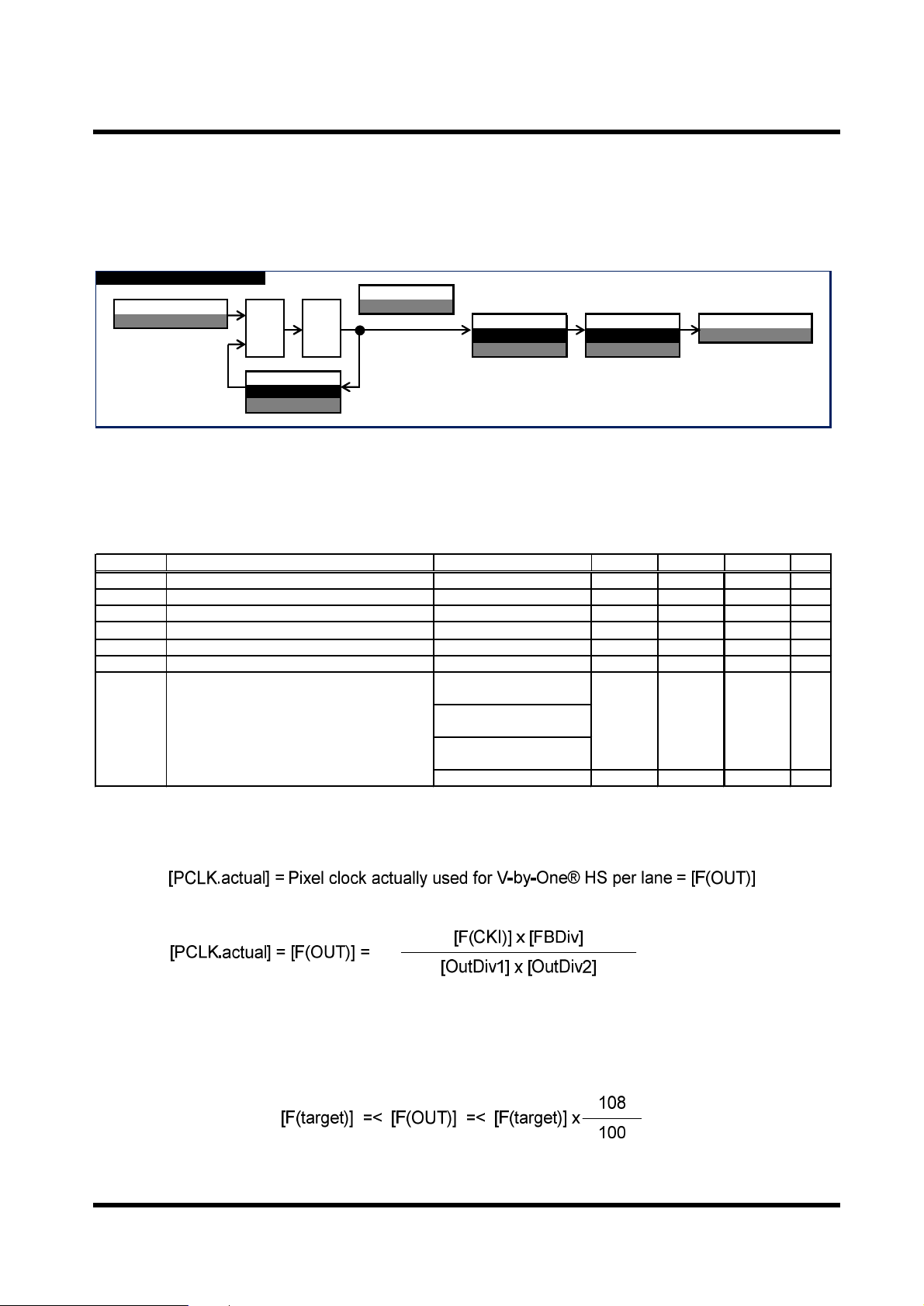
6.7 PLL setting
PLL setting is required. For manual setting, R_PLL_SET_MODE is supposed to be set 1 (Manual mode) from
default value 0. PLL Manual mode setting set R_PLL_SETTING[47:0] is related with CKI frequency.
Figure 5. Reference clock supply basic method
PLL_SETTING[47:0] must be selected proper to meet below constraints.
Table 16. PLL constraints table
Pixel clock frequency made by PLLis calculated as below.
Actual Pixel clock, F(OUT) frequency must be equal or greater than ideal target Pixel clock, F(target) by 8%
accuracy as below formula for most cases.
20-130
FeedBack Divider
x 1/FBDiv
2nd Output Divider
x 1/OutDiv2x 1/OutDiv1
1st Output Divider
1-7 1-7
F(Out)
10-133.3MHz
PLL Configuration F(VCO)
F(CKI)
PFD VCO
500-1300MHz
10-40MHz
symbol discription condition min typ max unit
F(CKI) CKIinput frequency - 10 - 40 MHz
FBDiv FeedBack Divider value - 20 - 130 -
OutDiv1 1st Output Divider value(OutDiv1 must be >= OutDiv2) - 1 - 7 -
OutDiv2 2nd Output Divider value(OutDiv1 must be>= OutDiv2) - 1 - 7 -
F(VCO) VCO frequency - 500 - 1300 MHz
F(OUT) PLL output pixel clock frequency - 10 - 133.3 MHz
Hactive=< 1280pixels
and [dmp]x[nmp] < 500Mbps
1280 <Hactive=< 1920pixels
and [dmp]x[nmp] < 800Mbps
1920 <Hactive=< 3840pixels
and [dmp]x[nmp] <1500Mbps
otherwise 0 0 8 %
DF|R_SPREAD| - 8 %
Allowed error between F(target) vs F(OUT)

Preliminary
THCV245A_Rev.0.90_E
Copyright©2020 THine Electronics, Inc. THine Electronics, Inc.
Security C
20/67
When transmitted camera image format horizontal active is rather large and total pixel data-rate is rather slow as
described in previous table condition, minimum allowed F(OUT) setting is not equal to F(target) if Spread
Spectrum function is activated. F is supposed to be more than absolute value of applied SSCG modulation rate,
|R_SPREAD|, under the condition specified on PLL constraints table.
Table of contents
Popular Extender manuals by other brands

PFPower
PFPower MAX IN-WALL MIW-XT installation instructions

Black Box
Black Box LB200A user manual

Black Box
Black Box ServSwitch ACU5114A Specifications

PULSEEIGHT
PULSEEIGHT neo LITE HDMI EXTENDER user manual

SMART-AVI
SMART-AVI LDX quick start guide

Black Box
Black Box IC282A Quick start guide and user manual


