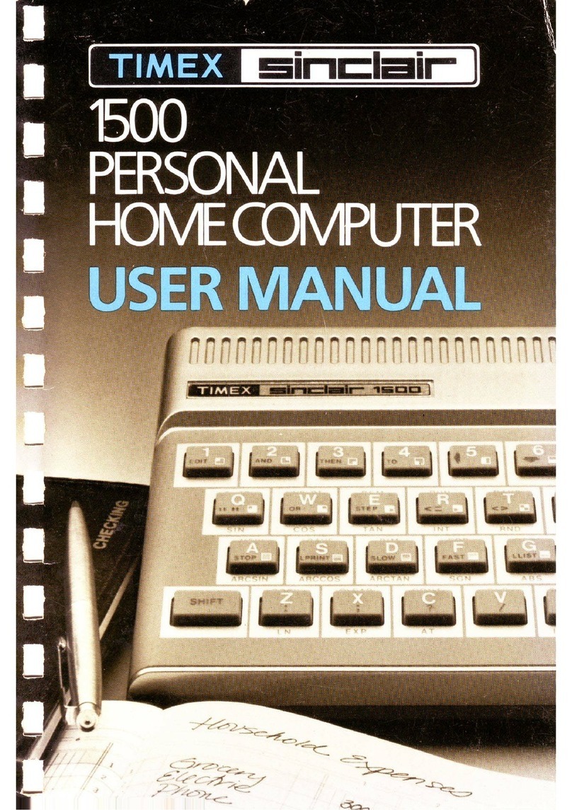
Timex Sinclair 2068 User manual

TECHNICAL
MANUAL
TIM EX SINCLAIR
2068
PERSONAL
COLOR COMPUTER
Published by The Time Designs Magazine Co


JOHN DONALDSON
mb roxwooocm
GENEVA, H. 10134
TIMEX SINCLAIR 2068
PERSONAL COLOR COMPUTER
TECHNICAL REFERENCE MANUAL
Prepared by
V. C. Corcoran
and
M. H. Branigin
TIMEX COMPUTER CORPORATION
Waterbury CT 06720
©May 1984
Second Edition Printing
Published Exclusively by:
TIME DESIGNS MAGAZINE CO.
COLTON, OREGON 97017
©JANUARY 1986

PREFACE
This manual is dedicated to the many individuals associated
with the Timex Computer Corporation in the development and
production of the TS2068. Our special thanks to Nan Parsons
who prepared the TS2068 Schematic and other drawings used
in this manual.
While every effort has been made to make this document
complete and accurate, use of the technical information
contained herein is at user's sole risk. The Timex Corp. or
its affiliates/ and Time Designs Magazine Company assume no
responsibility or liability for the safety or performance
of any product manufactured relying on the technical data
contained herein, or any liability, loss, damage, or
expense sustained by reason of any claim that such products
infringe any patent or other industrial property right.
The Second Edition of this Technical Manual has been re-
edited by Tim Woods. Special thanks to Bob Orrfelt and Dave
Clifford for technical assistance.
If you would like to receive information on amagazine and
other publications for the Timex Sinclair 2068, direct your
inquiry to: Time Designs Magazine Company, 29722 Hult Rd .
,
Colton, OR 97017.
Timex Sinclair 2068 Technical Manual (2nd Edition), OCopyright 1986 by the Time Designs
Magazine Company. Reproduction of this document In whole or In part by any means without
expressed written permission from Time Designs, Is prohibited by law.
This manual was printed by Toad' ILltho Printing and Composition, Oregon City, OR 97045.

TABLE OF CONTENTS
1.0 INTRODUCTION 1
1.1 TS 2068 Overview 1
1.1.1 Hardware Overview
1.1.2 System Software Overview
1.1.3 Cartridge Software Overview
2.0 HARDWARE GUIDE 7
2.1 Major Hardware Functions 7
2.1.1 AC Adapter
2.1.2 Voltage Regulation
2.1.3 Z80A CPU
2.1.4 ROM
2.1.5 32K RAM
2.1.6 Programmable Sound Generator
2.1.7 Joystick Port
2.1.8 Control Logic
2.1.9 Keyboard
2.1.10 16K Video Display RAM
2.1.11 Video Generation
2.1.12 Cassette I/O
2.1.13 Port Map
2.2 Schematic (see inside back cover and Appendix D)
2.3 Unit Absolute Ratings 53
2.4 Interfaces and Connectors 53
2.4.1 System Bus Connector -PI
2.4.2 Cartridge Connector -J4
2.4.3 Cassette I/O
2.4.4 Joystick
2.4.5 Composite Monitor Output
2.4.6 RF Output
2.4.7 Keyboard Interface Connector -J9
2.4.8 AC Adapter Power Plug
3.0 SYSTEM SOFTWARE GUIDE 65
3.1 Identifier 65

TABLE OF CONTENTS
(continued)
3.2 ROM Organization and Services 65
3.2.1 Home ROM
3.2.1.1
3.2.1.2
3.2.1.3
Fixed Entry Points
BASIC AROS Support
General
3.2.2 Extension ROM
3.2.2.1
3.2.2.2
3.2.2.3
3.2.2.4
Fixed Entry Points
General
Video Mode Change Service
Extension ROM Interface Routine
3.3 RAM Organization and Services 72
3.3.1 System Variables
3.3.2 System Configuration Table
3.3.3 Machine Stack
3.3.4 OS RAM Routines
3.3.4.1 RAM Interruption Handler
3.3.4.2 RAM Service Routines
3.3.4.3 Function Dispatcher
4.0 SYSTEM I/O GUIDE 91
4.1 I/O Channels 91
4.1.1 Keyboard
4.1.2 Video Screen
4.1.3 2040 Dot Matrix Printer
4.2 Cassette Tape 102
4.3 Joysticks 104
4.4 Software Generated Sound (BEEP) 105
4.5 Programmable Sound Chip (SOUND) 105
5.0 ADVANCED CONCEPTS 106
5.1 Cartridge Software/Hardware 106
5.2 Advanced Video Modes 117
5.3 Other 125

TABLE OF CONTENTS
(continued)
6.0 KNOWN "BUGS" AND CORRECTIONS 126
6.1 LROS and Machine Code AROS 126
6.2 Machine Code AROS 126
6.3 BASIC AROS 127
6.4 Video Mode Change Service 127
6.5 OS RAM Routines 129
6.6 General 134
APPENDICES
Appendix A-System ROM Maps/OS RAM Module 136
Appendix B-System Variables Definition File 150
Appendix C-Application Development Library 158
C-l
C-2
C-3
C-4
C-5 Dual Screen Mode
Spri tes
64-Column Mode
80-Column Mode
40-Column Mode
Appendix D-288
D-l
D-2
D-3
TS2068 PCB Assembly Drawing
TS2068 Parts List
TS2068 Schematic Diagram
Appendix E-Expansion Buss Comparisons 295
Appendix F-Modifications for EPROMs 296

LIST OF FIGURES
FIGURE NO. TITLE
1.1-1 TS 2068 Block Diagram
1.1-2 Memory Configuration
1.1-3 RAM Mapping
1.1-4 System Initialization Flowchart
2.1.3-1 CPU Timing
2.1.3-2 Op Code Fetch Timing
2.1.3-3 Memory Read/Write Timing
2.1.3-4 I/O Read/Write Timing
2.1.3-5 Interrupt Request/Ack. Cycle
2.1.4-1 Rework for EPROM's
2.1.6-1 PSG Register Block Diagram
2.1.6-2 Tone Period Registers
2.1.6-3 Noise Period Register
2.1.6-4 Mixer Control -I/O Enable Reg.
2.1.6-5 D/A Converter Signal Generation
2.1.6-6 Amplitude Control Registers
2.1.6-7 Variable Amplitude Control
2.1.6-8 Envelope Period Registers
2.1.6-9 Envelope Shape/Cycle Control Reg.
2.1.6-10 Envelope Generator Output
2.1.6-11 Envelope Generator Output Detail
2.1 .7-1 Joystick Port Operation
2.1.8-1 Bank Selection Logic
2.1.8-2 Video RAM Address Generation
2.1.9-1 Keyboard Schematic
2.1.10-1 Video RAM Data Organization
2.1.11-1 Composite Video Signal
2.4.1-1 PI Mating Connector Mechanical
Requi rements
2.4.1-2 PI Signal Layout
2.4.1-3 RGB Monitor Connection Schematic
2.4.2-1 J4 Mating Connector Mechanical
Requirements
2.4.2-2 J4 Signal Layout
2.4.4-1 Joystick Connector
2.4.8-1 AC Adapter Plug
3.2.2-1 Ext. ROM Interruption Fielder
3.2.2-2 Ext. ROM Interface Routine
4.1.1-1 Keyboard Mode Control
4.1.1-2 Keyboard Support Routines
Flowcharts
4.1.2-1 Standard Character Table Locations
4.1.2-2 Screen Row/Column Designations
4.2-1 Tape Header Formats
4.3-1 Joystick Data Format

LIST OF FIGURES
(continued)
FIGURE NO. TITLE
5.1-1 EPROM Cartridge Board Schematic
5.1-2 Ctdg.Bd. Component Side Artwork
5.1-3 Ctdg.Bd. Solder Side Artwork
5.1-4 EPROM Cartridge Bd. Solder Mask
6.5-1 GET_STATUS Corrections
6.5-2 PUT WORD Corrections
6.5-3 BANR_ENABLE and RESTOREJTATUS
Corrections
LIST OF TABLES
TABLE NO. TITLE
2-1 Z80A Control Signals
2.1.6-1 PSG I/O Enable Truth Table
2.1.6-2 PSG I/O Port Truth Table
2.1.8-1 SCLD I/O Pin Function Definitions
2.1.13-1 I/O Port Map
2.4.1-1 PI Signal Definitions
2.4.1-2PI Signal Electrical
Characteristics
2.4.2-1J4 Signal Definitions
2.4.2-2 J4 Signal Electrical
Characteristics
2.4.4-1 Joystick Connector Signal
Assignment
3.2.2-1 Inputs to Video Mode Change
Service
3.3.4-1 OS RAM Service Routines
3.3.4-2 Function Dispatcher Services
9


INTRODUCTION
This manual provides detailed technical Information on the T1mex
Sinclair 2068 Personal Color Computer. In conjunction with the TS2068
User Manual, It 1s Intended to assist the reader 1n understanding the
architecture, hardware and software features, programming techniques
and I/O techniques pertaining to the TS2068.
1.1 TS2068 Overview
1.1.1 Hardware Overview
Figure 1.1-1 is ablock diagram of the TS2068 showing the
major functional components and their logical
connections. These components are:
Control Logic -SCLD (Standard Cell Logic Device)
CPU -Z80A Microprocessor
RAM -48K Random Access Memory
ROM -24K System Read-Only Memory
(16K plus 8K Extension)
System Bus Connector
Cartridge Connector
Sound Generator/Speaker
Video Circuits
Cassette READ/WRITE
Joystick Connectors
The TS2068 Cartridge Connector provides for the plug-in
of cartridges containing programmed ROM's with up to 64K
of addressable memory. The full 64K is not normally
utilized (e.g., due to need for access to RAM for the
machine stack). See Section 5.1 for details.
Figure 1.1-2 shows the standard TS2068 memory
configuration comprised of the Home Bank, the ROM
Extension Bank and the Dock (Cartridge) Bank. This
memory is selectable as eight 8K 'chunks' with the Home
Bank being enabled by default, I.e., any chunk not
selected in the Extension or Dock Bank 1s automatically
enabled In the Home Bank.
Memory selection and I/O are controlled via the I/O
ports. These topics are covered in detail in later
sections.

FIGURE 1.1-1
TS 2068 SYSTEM BLOCK DIAGRAM
WALL AC
ADAPTER
VOLTAGE
REGULATOR
+12V
+5V
GNO
16K
RAM
Control
VDEO
cwcurrs
COLOR \_
CRYSTAL^
3.S79S46 MHZ
(monttor)
Of
KEYBOARD MATRIX
u
CENTRAL LOGIC
v
A
V
A-
V
32K
RAM
16K
RAM
8K
RAM
Data
Addroaa
Control
IZ-60A CPU ACARTRCGE A(SYSTEM BUS A
11CONNECTOR JCONNECTOR ^
JOYSTICKS
FIGURE 1.1-2
TS 2068 STANDARD MEMORY CONFIGURATION
7
6
5
4
3
2
1
a
aooress
FFFFM
EM6H
C0MH
8<WtN
60MM
40MH
2W*H
RAM
RAM
ROM
ROM
HOME BANK
(BANK *255) EXTENSION BANK
(BANK *254)
ROM
ROM
ROM
ROM
ROM
ROM
ROM
ROM
UP TO B4K
1FuU 64K addrMting *pac«
not normally utIHzed.
S*« Socllon S.t
CARTWOGE
(DOCK)
BANK
(BANK *•)
2

1.1.2 System Software Overview
The TS2068 System Software resides in the Home ROM, the
Extension ROM, and dedicated RAM. It supports the
following functions:
-System Initialization
-BASIC Interpreter (including BASIC cartridge support)
-BASIC I/O for Standard Peripherals
okeyboard
ovideo screen
o2040 32-col. dot matrix printer
ocassette tape
ojoysticks
osoftware generated sound (BEEP)
oprogrammable sound chip (SOUND)
-Video Mode Change Service
-Interruption Servicing (Z80 Int. Mode 1)
-Bank Switching/Data Transfer Services
-Function Dispatcher (provides access to selected system
routines via aService Code input)
In addition, portions of the Home Bank RAM are used for
the machine stack, the BASIC system variables, the
Printer Buffer and the Display Files. Figure 1.1-3 shows
the standard mapping of the Home Bank RAM and the mapping
necessary when the second display file is to be used with
the BASIC interpreter still functional. The Video Mode
Change Service routine makes these memory modifications.
Note that there is no direct support of the second
display file via BASIC or in the system ROM I/O routines.
Figure 1.1-4 is aFlowchart of the System Initialization
process.
3

FIGURE 1.1-3
STANDARD MAPPING OF
HOME BANK RAM
P-RAMT
RAMTOP UDG
STKENO
STXBOT
WORKSP
E-LME
VANS
PROG
CHANS
ARS8UF
6S40M
62MH
60MH
5C0«H
saoan
490SH
(MACHINE COPE VARIABLES)
OS RAM-RESDENT CODE
MACHINE STACK
SYSTEM VARIABLES
PRINTER BUFFER
[XSPLAY HLE 1
HOME ROM
A) 1Display Fas
OS RAM-RESCENT CODE
MACHMC STACK
UDG
(MACH—ICODE VAWWJLES)
DISPLAY FU 2
SYSTEM VARMBLES
PRBfTER BUFFER
DISPLAY FTLE I
P-RAMT
•F9COH
BF7COH
RAMTOP
STKEND
STXBOT
WORKSP
E-LME
VARS
PROG
CHANS
ARSBUF
7»MH
SCMH
SBOOH
4MOH
B) 2Display FHa
4

FIGURE 1.1-4
SYSTEM INITIALIZATION
CPOWER ON
C )
HOME ROM
SET MAX.
ADDRESS -64K
EXTENSION ROM
SET MAX.
ADDRESS r64K
Switch to Horn* Rotnl
INITIALIZE
CHANS/STREAMS
tPRINTER BUFFER
CLEAR SCREEN
•OUTPUT
(C) MSG.
COPY OS RAM
CODE TO CHUNK 3Switch to Entantlon
5
t

1.1.3 Cartridge Software Overview
The TS2068 supports two basic types of Cartridge or
ROM-Oriented Software designated as LROS (Language
ROM-ORiented Software) and AROS (Application ROM-Oriented
Software) which plug into the cartridge connector. They
are identified via overhead bytes at Location 0for an
LROS or 32768 (8000H) for an AROS. The fundamental
difference is that an LROS contains Z80 machine code in
memory chunk 0and is in total control of the TS2068
hardware including the RESTART implementation and
Interruption Mode setting and handling, while an AROS is
dependent on the System ROM or an LROS for these
functions if needed. An AROS written in BASIC, which may
also include machine code accessed via the USR function,
is supported from the System ROM BASIC Interpreter and is
mapped beginning in memory chunk 4. An AROS may also be
written entirely in Z80 machine code. An AROS written in
any other high-level language would require an LROS
supporting that language and would have to be integrated
with the LROS in a single cartridge.
See Sections 3.2.1.2, BASIC AROS Support and 5.1,
Cartridge Software/Hardware, for additional details.
6

2.0 HARDWARE GUIDE
2.1 Description of Major Hardware Functions
Figure 1.1-1 shows asimplified block diagram of the TS2068. The
following functional units are described in the following
bcL 11Ulib .
SECTION FUNCTIONAL 1INTT
911
C.I.I ml. Muapter
C. \.Cvoiuage Keguiai-ion
9i
£.1.0 i-oUM L»ru
91^1
C. 1.0.
1
naa ma ^t+ D#»
Aaaress bus
91^9
C. I.O. CUdLd BUS
C. I.J.J uontroi oignais
C. 1.O. HAD Caf
ur L.ooe reicn
C. 1.O. 3Mamnvu nr An /UD TTF
c. 1.J.
O
T/fl DFAn/UDTTF
l/U KCMLI/WK X1
£
?n7
c. •1•O•/Mac^aHlo Tntavtviinfi' nn
ndsNau ic inLcrruption
91^Q
c. 1.0. oNon-MasKaDie interruption inmij
91Annu
KUM
91K
(1.1.0 oot/ DAM
oils. KAM
91C
£.1.0 Sound Generator
917
C.I./ joystick Port
91ft L.ontrui Logic.
2.1.8.1 Bank Selection Logic
2.1.8.2 Z80 Clock Generator
2.1.8.3 Display File Access
2.1.8.4 Interruption Generation
2.1.9 Keyboard
2.1.10 16K Video Display RAM
2.1.11 Video Generation
2.1.11.1 Composite Video
2.1.11.2 RF Modulator
2.1.12 Cassette I/O
2.1.13 Port Map
7

2.1.1 AC Adapter
The AC Adapter transforms 117V AC (Nominal) to filtered
DC via astep down transformer, full -wave bridge
rectifier, and filter capacitor to supply from 14 to 25
volts at 1amp over the AC voltage variation range of 105
to 130 VAC. Transformer isolation exceeds 1500 volts.
117v
AC 60Hz.
14 to 25v
DC
2.1.2 Voltage Regulation
Unregulated DC from the AC Adapter is supplied for
regulation through abi -filar torroidal inductor which
reduces conducted line emanation for FCC compliance and
through the power-ON/OFF switch located on the left side
of the TS2068. This switch voltage is supplied to the
System Bus Connector (see Section 2.4) and for regulation
to the +12 Vregulator and the +5 Vregulator.
Characteristics are as follows:
SUPPLY VOLTAGE RANGE CURRENT RANGE
5V 4.75 -5.25V
12V 11.5 -12.5V 200ma -1.0 A
20ma -lOOma
JWWYVv.
14 to 25v
DC fwvwv\_ REGULATOR
>+20v
-» +5v
>+12v
-> GND
8

The 12V regulator is a 78L12 series regulator while the
5V regulator is a switching supply utilizing the 78S40
circuit.
2.1.3 Z-80A CPU
The Z-80A CPU of the TS2068 operates at aclock frequency
of 3.53 MHz. Primary features of this CPU are:
158 instructions
Dual register set
Two index registers
On-chip refresh logic
The Z-80 CPU executes instructions by proceeding through
asequence of operations that include:
a) instruction Op code fetching
b) READ or WRITE memory
c) READ or WRITE I/O
d) Acknowledge an interruption
The basic clock period is referred to as aTtime or
state and three or more Tstates make up amachine
cycle. In the TS2068, each T-time is approximately 283
nanoseconds (2.83 X10~7seconds). Figure 2.1.3-1
illustrates the basic timing.
FIGURE 2.1.3-1
BASIC CPU TIMING EXAMPLE
9

2.1.3.1 Address Bus
Output from the Z-80 are 16-blts of address
Information, AO -A15, which are high-active
tr1 -state signals and address for memory data
and I/O device exchanges.
2.1.3.2 Data Bus
These Input/output signals from the Z-80, DO -
D7, constitute an 8-b1t bi-directional,
high-active, tri -state data bus used for data
exchanges with memory and I/O devices.
2.1.3.3 Control Bus
Associated with the Z-80 are 13 control lines
which are provided by or used by the Z-80 to
control system operation. These signals are
detailed 1n Table 2-1.
2.1.3.4 Op Code Fetch
The timing during an Ml cycle (OP Code Fetch)
is shown in Figure 2.1.3-2. At the beginning
of the Ml cycle the PC (Program Counter) is
placed onto the address bus, then one-half
clock time later the MREQ signal goes active
indicating that the memory address is stable.
The RTJ signal 1s activated to indicate that
memory read data should be gated onto the data
bus. At the rising clock edge during the T3
state, the CPU samples the data onthe data bus
and deactivates the ~R"D~ and MKETf signals.
During the T3 and T4 states, the CPU decodes
and executes the fetched instruction and the
CPU places on the lower 7bits of the address
bus amemory refresh address and activates the
RFSH signalindicating arefresh read is to
begin when MREQ 1s activated.
2.1.3.5 Memory READ/WRITE
Memory read or write cycles other than Op Code
Fetches are 3clock periods long with the WrUJ
and R~D~ signals used as in the fetch cycle.
During awrite cycle the Wsignal Is activated
when the write data is stable on the data bus.
The address and data bus contents remain stable
for one-half T state after the WT signal goes
active. Figure 2.1.3-3 illustrates.
10
Table of contents
Other Timex Sinclair Desktop manuals
