Transphorm TDINV1000P100 User manual

August 3, 2017 © 2017 Transphorm Inc. Subject to change without notice.
evk006.2
1
User Guide
TDINV1000P100: 1kW Inverter Evaluation Board
Introduction
The TDINV1000P100 1kW inverter kit from Transphorm provides an easy way to evaluate the performance advantages of GaN
power transistors in various inverter applications, such as solar and UPS. The kit provides the main features of a single-phase
inverter in a proven, functional configuration, operating at or above 100kHz. At the core of the inverter are four 150mΩGaN
FETs configured as a full bridge. These are tightly coupled to gate-drive circuits on a board which also includes flexible
microcontroller options and convenient communication connection to a PC. The switch-mode power signals are filtered to
provide a pure sinusoidal output.
The TDINV1000P100-KIT is for evaluation purposes only.
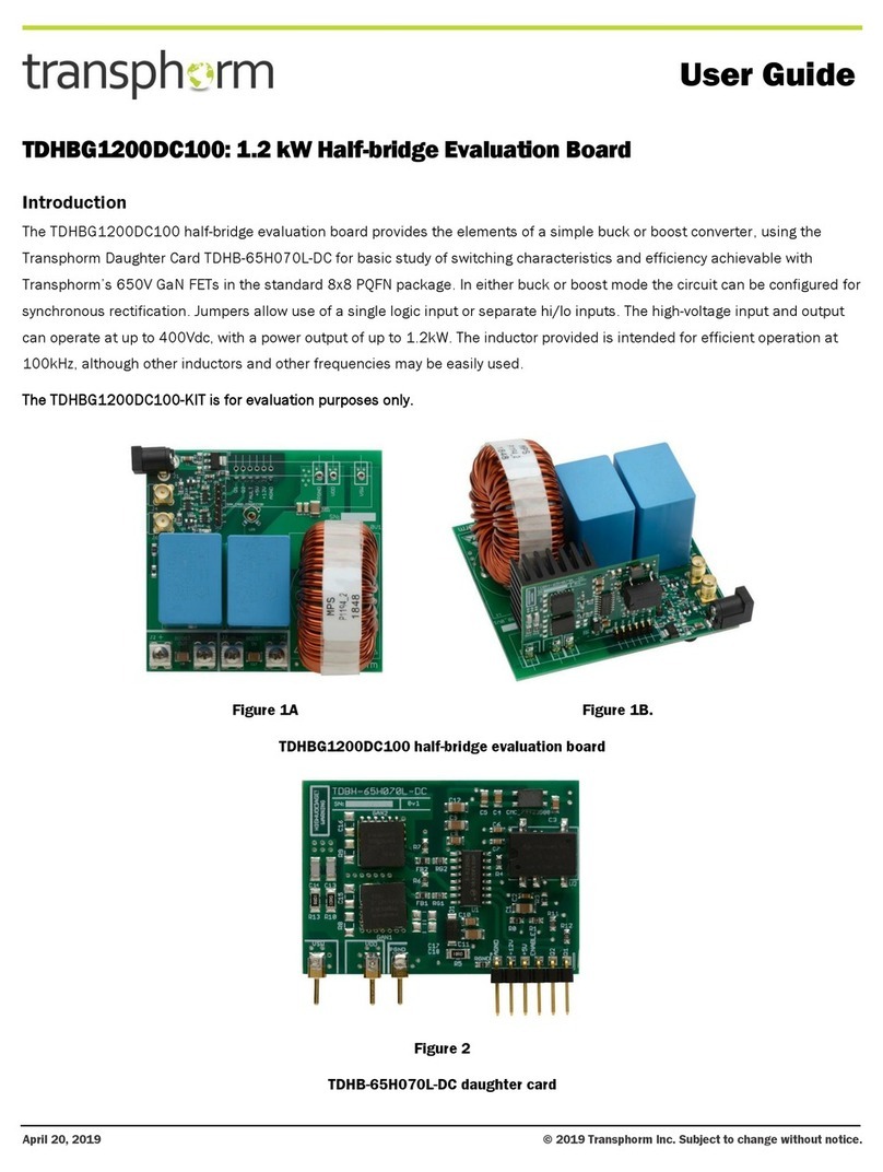
Figure 1. TDINV1000P100 inverter evaluation board
The control portion of the circuit is designed around the popular C2000™ family of microcontrollers from Texas Instruments (TI).
The source code is available along with related support information directly from TI. In addition to this general resource,
Transphorm provides original firmware which comes loaded in flash on the microcontroller. The source code, configured as a
complete project, is also available at transphormusa.com/pv1fw. This project is a convenient starting point for further
developments. The microcontroller itself resides on a small, removable control card, supplied by TI, so that different C2000
devices may be used if desired. The schematic for the TDINV1000P100 circuit board is provided at the end of this user guide
document, as well in thedesign files attransphormusa.com/pv1kit.

August 3, 2017 transphormusa.com
evk0006.2
2
TDINV1000P100 User Guide
The TDINV1000P100-KIT includes:
•TDINV1000P100 single phase inverter assembly
•Texas Instrument F28035 control card
•9V power supply
TDINV1000P100 input/output specifications
High-voltage input: 400VDC max
Auxiliary supply (J1): 9VCC
Input: 0VDC - 400VDC
Output: VDC / √2VRMS at 50/60Hz 1, up to1000VA
PWM frequency: 100kHz - 300kHz 2
1The$output$frequency$may$be$changed$in$the$software;$as$delivered$it$is$60Hz
2The$switching$frequency$may$be$changed$in$the$software;$as$delivered$it$is$100kHz
Power dissipation in the GaN FET is limited by the maximum junction temperature. Refer to the TPH3206PSB datasheet.
Circuit description
Refer to Figure 2 for ablock diagram of the inverter circuit. Adetailed schematic is also available in the design files at
transphormusa.com/pv1kit.
The TDINV1000P100 inverter is a simple full-bridge inverter. Two GaN half-bridges are driven with pulse-width modulated
(PWM) command signals to create the sinusoidally varying output. The output filter largely removes the switching frequency,
leaving the 50/60Hz fundamental sinusoid. The high-frequency (100kHz+) PWM signals are generated by the TI microcontroller
and connected directly to high speed, high voltage gate drivers. Aconnection for external communication to the microcontroller
is provided byanisolated USB interface. Except for thehigh-voltage supply for the power stage, all required voltages for the
control circuitry are derived from one 9V input.

August 3, 2017 transphormusa.com
evk0006.2
3
TDINV1000P100 User Guide
Figure 2. Circuit block diagram
The inverter takes advantage of diode-free operation, in which the freewheeling current is carried by the GaN FETs themselves,
without the need of additional freewheeling diodes.For minimum conduction loss, the gates of the transistors are enhanced
while they carry the freewheeling current. The high and low-side VGS waveforms are therefore pairs of non-overlapping pulses, as
illustrated in Figure 3 below.
Figure 3. Non-overlapping gate-drive pulse; A is a deadtime set in the firmware
Gate drivers
High-voltage integrated drivers supply the gate-drive signals for the high and low-side power transistors. These are 2500V
isolation drivers (Silicon Labs Si827x family), specifically chosen for high-speed operation without automatic deadtime insertion.
The deadtime between turn-off of one transistor in a half bridge and turn-on of its mate is set in the firmware.
Hi/Lo
Gate
Driver
V
P
V
N
Hi/Lo
Gate
Driver
V
P
V
N
Hall Sensor
Current
Voltage
Feedback
GaN
Half-bridge Filter
AC
Output
TMS320F28069
Microcontroller
Power Stage
controlCARD
V
SENSE
(HV
DC
)
Feedback4
5
2
Isolated USB
Interface
JTAG
UART
V
P
V
N
High Voltage
DC Input
+V
GG
+5V +3.3V
V
N
Low Voltage Supply
9V
CC
-15V
CO
Input

August 3, 2017 transphormusa.com
evk0006.2
4
TDINV1000P100 User Guide
Output filter
A simple LCL filter on the output (L3, L4, C37 and C54 - C57) attenuates the switching frequency, producing a clean sinusoidal
waveform for output connections in terminals J4 and J5. The filter inductors and capacitors used on the demo board were
chosen to provide the optional combination of benefits: low loss, good attenuation of the switching frequency, and small size.
Consult the schematic and/or bill of materials to verify values; but in general, the cutoff frequency will be around 5 - 10kHz to
accommodate 100kHz switching. The inductors have powder cores with relatively low permeability (60-90) and soft saturation
characteristics. The inductors and/or capacitors can be changed to evaluate different filter designs.
Current sensing
Hall sensors U8 and U10 provide linear current feedback to the microcontroller. These signals could be used to control output
power flow, and/or to protect against short circuits. The firmware provided with the kit, however, does not actually make use of
this feedback. Note that these are placed at an intermediate point of the output filter. Refer to the bill of materials to confirm
the sensor part numbers, but typical would be the Allegro ACS712-20A sensor, which has a ±20A range (100mV/A). These parts
are pin compatible with a ±5A and ±30A versions of ACS712, should higher or lower ranges be desired. Note also that resistor
dividers scale the 5V outputs for the 3V range of the A/D.
Communication
Communication between the microcontroller and a computer is accomplished with a standard USB cable. The isolated USB
interface enables simultaneous operation of two physical ports to the microcontroller: a JTAG port for debug and loading of
firmware, and a UART for communication with a host application.
Control card
The microcontroller resides on a removable card, which inserts in a DIM100 socket on the inverter PCB. The socket can accept
many of the C2000 series control cards from Texas Instruments. The TMDSCNCD28035 Piccolo control card supplied with the
kit provides capability to experiment with a wide variety of modulation and control algorithms. It comes loaded with firmware to
allow immediate, out-of-the-box, operation. Should the user wish to use an alternative microcontroller family, an appropriate
control card can be designed to insert into the DIM100 socket.
Heat sink
The two TO-220 GaN transistors on each half-bridge are mounted on a common heat sink. The heatsink is adequate for 1000W
operation WITHOUT forced air flow. Even higher efficiency at high power may be achieved by minimizing the temperature rise.
This may be accomplished with forced airflow. Alternately the heatsinks could be replaced with larger and more effective ones.
Connections
Power for the AC output is derived from the high voltage DC input. This will typically be a DC power supply with output voltage up
to 400VDC. A 22µF, low ESR, film capacitor is provided as a bypass capacitor for the high voltage supply, along with several
smaller value ceramic capacitors in parallel. This is not intended to provide significant energy storage, but to provide high
frequency bypassing. It is assumed that the power supply or preceding DC-DC stage contains adequate output capacitance.
The control, communication, and gate-drive circuits are all powered from a single 9V input (VGG). A wall-plug adaptor is provided.

August 3, 2017 transphormusa.com
evk0006.2
5
TDINV1000P100 User Guide
Note that only the USB port is isolated; all other signals on the board are referenced to the negative terminals of the high and
low voltage supplies, which are tied together on the PCB. The heatsinks are also connected to the negative terminals of the
supplies.
Connection sequence
Refer to Figure 4. Insert the microcontroller card to the DIM100 socket before applying any power to the board. To use the
preloaded firmware, verify that jumper JP1 is removed. This releases the JTAG port and allows the microcontroller to boot from
flash. For communication with a host over the JTAG port, JP1 should be installed.
With the supply turned off, connect the high-voltage power supply to the +/- inputs (J2 and J3).
DO NOT apply too much force to
the J2 and J3 connectors, as excessive force may bend and/or crack the PCB.
If a load is to be used, connect the load to the output terminals (J4 and J5).
DO NOT apply too much force to the J4 and J5
connectors, as excessive force may bend and/or crack the PCB.
Insert the VGG (9V) plug to jack J1. LED1 should illuminate, indicating power is applied to the 5V and 3.3V regulators. Depending
on the specific control card used, one or more LEDs on the control card will also illuminate, indicating power is applied. A
flashing LED indicates the firmware is executing.
To use the pre-loaded firmware, no computer connection is required. If a computer connection is required for code modification,
connect the USB cable from the computer to the USB connector (CN3). LED2 should illuminate, indicating isolated +5V power is
applied over the USB cable.
Turn on the high voltage power. The high-voltage supply may be switched ON instantly or raised gradually.
Figure 4. Connections

August 3, 2017 transphormusa.com
evk0006.2
6
TDINV1000P100 User Guide
Test
Figure 5 shows typical waveforms. The negative terminal of the high-voltage supply is a convenient reference for the
oscilloscope measurements, provided there are not multiple connections to earth ground.
Typical efficiency results are shown in Figure 6. These data points correspond to efficiency measurements made in still air with
20 minutes’ dwell at each power level. Input power from the 350VDC source and output power to a resistive load were measured
with a Yokogawa WT1800 power analyzer.
Figure 5. Typical waveforms
Driver
Driver
Single-phase
240V
AC
Output
MCU
100kHz switching waveform Yellow: Load current using current probe
Green and Purple: Phase output voltages
with respect to higher voltage (-) input

August 3, 2017 transphormusa.com
evk0006.2
7
TDINV1000P100 User Guide
Figure 6. Typical efficiency: 350VDC input, 240VAC output
Design details
See Figure 7 for adetailed circuit schematic and Figure 8 for the PCB layers (also included in the design files). The parts list can
be found in Table 1.
Table 1. TDINV1000P100 evaluation board bill of materials (BOM)
Designator
Qty
Value
Description
Part Number
Manufacturer
X1
1
CSTCR
CSTCR6M00G53Z-R0
Murata
HS1, HS2
2
529802B02500G
529802B02500G
Murata
D1, D2
2
DO-214AC
ES1J
Aavid Thermalloy
FB1, FB2, FB3, FB4
4
120Ωferrite bead
603
MMZ1608Q121B
Fairchild
LED1, LED2
2
CHIP-LED0805
SML-211UTT86
TDK
C49, C53
2
0.1µF
C1812
C1812V104KDRACTU
ROHM
C1, C14, C16, C17,
C19, C20, C21, C22,
C23, C24, C25, C26,
C27, C28, C29, C30,
C31, C33, C34, C38,
C39, C40, C42, C43
24
0.1µF
C0603
06033C104JAT2A
Kemet
C5, C6, C7, C8, C9
5
0.1µF
C0805
08053C104KAT2A
AVX
C10, C54, C55, C56,
C57
5
0.1µF
C2225K
VJ2225Y104KXGAT
AVX
R21, R28
2
DNI
R0603
DNI
Vishay
R7
1
0Ω
R1206
ERJ-8GEY0R00V
Panasonic
R14
1
1MΩ
R0603
ERJ-3EKF1004V
Panasonic
R8, R15
2
1kΩ
R0603
CRCW06031K00FKEA
Vishay
R1
1
1kΩ
R0805
ERJ-6GEYJ102V
Panasonic
C36, C45
2
1nF
C0603
DNI
AVX
C12, C18
2
1µF
C0603
CC0603KRX5R6BB105
Yageo
C15
1
2.2µF
C0603
0603YD225MAT2A
AVX
R13, R17
2
2.2kΩ
R0603
ERJ-3GEYJ222V
Panasonic
C46, C47, C48, C50,
C51, C52
6
4.7nF
C1206
C1206C472KDRACTU
Kemet
R19, R26
2
5.23kΩ
R0603
ERJ-3EKF5231V
Panasonic
R6, R24, R31
3
9.09kΩ
R1206
ERJ-8ENF9091V
Panasonic
R18, R25
2
10Ω
R0805
ERJ-6GEYJ100V
Panasonic

August 3, 2017 transphormusa.com
evk0006.2
8
TDINV1000P100 User Guide
Designator
Qty
Value
Description
Part Number
Manufacturer
R22, R29
2
10.2kΩ
R0603
ERJ-3EKF1022V
Panasonic
R5
1
10MΩ
R1206
HVCB1206FKC10M0
Stackpole
R12, R16
2
10kΩ
R0603
ERJ-3GEYJ103V
Panasonic
C32, C35, C41, C44
4
10µF
C0805
C0805C106M4PACTU
Kemet
C4
1
10µF
C1206
CL31A106KAHNNNE
AVX
C2
1
22µF
C1206
CL31X226KAHN3NE
Samsung Electronics
L1, L2
2
22µH
805
LQM21FN220N00L
Murata
R10, R11
2
27Ω
R0603
CRCW060327R0FKEA
Vishay
U6
1
93LC46B
SOT23-6
93LC46BT-I/OT
Microchip
R2
1
348Ω
R0805
ERJ-6ENF3480V
Panasonic
R9
1
470Ω
R0603
ESR03EZPF4700
ROHM
R3, R4, R20, R23,
R27, R30
6
560kΩ
R1206
RC1206FR-07560KL
Yageo
U8, U10
2
ACS712
SO8
ACS712ELCTR-20A-T
Allegro Microsystems
DA1
1
BAW567
SOT363
BAW567DW-7-F
Diodes Inc
U5
1
FT2232D
LQFP48
FT2232D-REEL
FTDI
IC1
1
ISO7240
SO-16DW
ISO7240CDW
Texas Instruments
IC2
1
ISO7242
SO-16DW
ISO7242CDW
Texas Instruments
U4
1
LVC2G74
DCT
SN74LVC2G74DCTR
Texas Instruments
U7, U9
2
SI8273AB1
SOIC16N
SI8273AB1
Silicon Labs
U3
1
TPS73033
SOT23-5
TPS73033DBVR
Texas Instruments
U1
1
TPS79533
SOT223-6
TPS79533DCQR
Texas Instruments
J2, J3, J4, J5
4
KEYSTONE_7691
7691
Keystone
2
Q1, Q3 insulator
SP2000-0.015-00-54
Bergquist
2
Q2, Q4 insulator
53-77-9G
Aavid Thermalloy
C11
1
MKP1848622454P4
MKP1848622454P4
MKP1848622454P4
Vishay
U2
1
PTH08080WAH
PTH08080W_TH
PTH08080WAH
Texas Instruments
C13
1
100nF
C075-032X103
SA111E104MAR
AVX
C37
1
2µF/630V
EPCOS_B32674
B32674D6225K
Epcos
JP1
1
1X02
961102-6404-AR
3M
J1
1
PJ-002AH
PJ-002AH
CUI Inc
CN2
1
USBSHIELD
897-43-004-90-000000
Mill-Max
C3
1
100µF
PANASONICSMALCAP6X6
EEE-FPE101XAP
Panasonic
plastic shoulder
washers
4
plastic shoulder
washers
plastic shoulder washers
3049
Keystone
CONN SHUNT 2POS
.100
2
jumper
CONN SHUNT 2POS .100
65474-002LF
FCI
#4-40, 3/8" Phillips
pan head screw
2
#4-40, 3/8" Phillips
pan head screw
#4-40, 3/8" Phillips pan
head screw
9901
Keystone
#4-40 hex nut
1
#4-40 hex nut
#4-40 hex nut
4694
Keystone
standoffs 4-40 5/8"
4
standoffs 4-40 5/8"
standoffs 4-40 5/8"
1902F
Keystone
Q1, Q2, Q3, Q4
4
TPH3206PSB
TPH3206PSB
TPH3206PSB
Transphorm
1
Control card Piccolo
F28035
Control card Piccolo
F28035
TMDSCNCD28035
Texas Instruments
L3, L4
2
295µH inductor
295µH inductor
CWS-1SN-12471
CWS
CN1
Control card connector
control card connector
TMDSDIM100CON5PK
Texas Instruments
1
9V adaptor
Accessory
CUI
CUI
4
Nylon screw for
standoffs
nylon screw for standoffs
9330
Keystone

August 3, 2017 transphormusa.com
evk0006.2
9
TDINV1000P100 User Guide

August 3, 2017 transphormusa.com
evk0006.2
10
TDINV1000P100 User Guide

August 3, 2017 transphormusa.com
evk0006.2
11
TDINV1000P100 User Guide
Figure 7. Detailed circuit schematics

August 3, 2017 transphormusa.com
evk0006.2
12
TDINV1000P100 User Guide
(a) PCB top layer
(b) PCB bottom layer

August 3, 2017 transphormusa.com
evk0006.2
13
TDINV1000P100 User Guide
(c) PCB inner layer 2 (ground planes) and inner layer 3 (power plane)
Figure 8. PCB layers
Probing
There are no test points provided for probing the low-side gate or half-bridge switching node. To minimize inductance during
measurement, the tip and the ground of the probe should be directly attached to the sensing points to minimize the sensing
loop. For safe, reliable, and accurate measurement, a scope probe tip may be directly soldered to the low-side FET drain and a
short ground wire soldered to the low-side FET source. See Figure 9 for an alternative that does not require soldering the probe
tip.
Warnings
There is no specific protection against over-current or over-voltage on this board. The TDINV1000P100 board is for evaluation
purposes only.

August 3, 2017 transphormusa.com
evk0006.2
14
TDINV1000P100 User Guide
Figure 9. Low-inductance probing of fast, high-voltage signals
Table of contents
Other Transphorm Motherboard manuals

