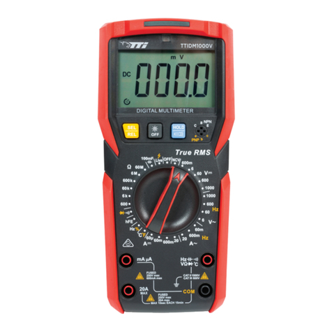
TTI 1906 User manual

1906
Multimeter
Service Manual
Part Number 48511-1110 Iss.2

Specification
Accuracy
Accuracies apply for 1 year 18°C to 26°C. Temperature coefficient outside these limits is <0.1x quoted
range accuracy per °C. Warm-up time to rated accuracy is 1 hour.
DC VOLTS
Range Accuracy Input Impedance Max Input
200Mv 0.017% + 3D 10MΩor 1kV DC or
2V 0.012% + 3D >1GΩAC Peak,
20V 0.019% + 3D 10MΩany range
200V 0.019% + 3D
1000V 0.019% + 3D
RESISTANCE (OHMS)
Range Accuracy Max. Measuring Current Max Input
200 0.025% + 4D 1.5mA
2k 0.019% + 3D 1.5mA 300V DC or RMS
20k 0.019% + 3D 0.4mA continuous,
200k 0.019% + 3D 40uA any Ohms input,
2M 0.022% + 3D 4uA any range
20M 0.07% + 3D 400nA
Max open circuit voltage 3.5V.
Audible continuity check available on all ranges.
TRMS AC VOLTS
Range Accuracy
Range Accuracy
45Hz - 5kHz 5kHz - 10kHz 10kHz - 20kHz 20kHz - 50kHz
200mV 0.2% + 150D 0.2% + 250D 3% + 500D -
2V 0.2% + 150D 0.2% + 250D 0.5% + 300D 3% + 1500D
20V 0.2% + 150D 0.2% + 250D 0.5% + 300D 2% + 1000D
200V 0.2% + 150D 0.2% + 250D 0.5% + 500D -
750V 0.2% + 150D - - -
Additional error at crest factor=3 typically 0.7%
Input impedance 1MOhm//<100pF any range.
Max input 750V rms, 1kV peak, any range.
2

AMPS
Range Accuracy Voltage Burden Max Input
200uA 0.08% + 12D 1A,300V
2mA 0.08% + 12D 300mV max fuse protected
20mA 0.08% + 12D
200mA 0.08% + 12D
10A up to 2000mA 0.06% + 10D 650mV max 10A, 300V
above 2000mA 0.12% + 10 fuse protected
TRMS AC AMPS
Range Accuracy 45Hz - 1kHz Voltage Burden Max Input
200uA 0.37% + 100D 1A,300V
2mA 0.37% + 100D 300mV max fuse protected
20mA 0.37% + 100D
200mA 0.37% + 100D
10A up to 2000mA 0.34% + 100D 10A, 300V
above 2000mA 0.4 % + 100D 650mV max fuse protected
Additional error at crest factor=3 typically 0.7%.
DISPLAY
Display Type: 13mm LED, 8 digit.
Scale Length: Selectable 5½ digit or 4½ digit.
Reading Rate: 3 readings/sec (5½ digit).
10 readings/sec (4½ digit).
Overange Indication: Displays -OL- if input too great for range.
Overflow Indication: Displays OFLO if calculated result too large for display.
Annunciators: LED annunciators for range, function and program modes.
Input Characteristics
Input Current: <100pA.
DC NMR: >60dB at 50/60Hz.
1k Unbalanced CMR: >120dB at DC/50Hz/60Hz, DC ranges;
>60dB at DC/50Hz/60Hz, AC ranges;
Hi Z: Switchable high impedance (>1GOhm) on 200mV and 2V DC ranges.
COMPUTING FUNCTIONS
Null: Operates over full range; values can be stored for every function.
Digital Filter: 10 options, including optimised default values for each range and function.
T/HOLD
(Touch & Hold): Reading is held when stable.
% DEV: Displays % deviation from entered reference value.
3

dB: Displays measurement in dB relative to 1V, 1mA, 1kOhm or user entered
value, or in dBm.
Ax+B: Linear scaling of results, with offset.
Limits: Reading displayed with 'H','L',or'P' (pass) with respect to user-defined high
and low limits.
Min/Max: Minimum and maximum reading stored.
Data Logger: Manual or automatic storage of 100 measurements.
INTERFACES
RS232: Complies fully with the ARC (Addressable RS232 Chain) interface
standard. Address selectable from the front panel. Baud rates 9600, 1200
and 300
GPIB (Optional): Fully complies with IEEE-488.2
POWER REQUIREMENTS
AC Input: 110/120 Volts AC nominal 50/60Hz or 220/240 Volts AC nominal 50/60Hz
by rear panel adjustment. The instrument will operate safely and meet
specification within normal AC supply variations, viz. 99-132 Volts AC and
198-264 Volts AC respectively.
Power Consumption: 25VA max.
Safety
This multimeter DMM is a Safety Class I instrument by IEC classification; it has been designed to meet
the requirements of both IEC348 and IEC1010-1.
This multimeter has been designed for use in a Pollution Degree 1 environment in the temperature
range 5°C to 40°C, 20% - 80% RH (non-condensing). It has been designed for Installation Category
II measurement use to 600VDC/rms and Installation Category I measurement use to 1000V DC/rms.
General
Environmental
Operating Range: +5°C to +4°C, 20% to 80% RH
Environmental
Storage Range: –40°C to +60°C
Size: 260(W) x 88(H) x 235(D)mm, excluding handle and feet
Weight: 2.2kg.
4

Safety
When operating the instrument with the covers off the users attention is drawn to the fact that the
measurement circuit analogue common is capable of being driven up to 1kV above earth ground.
All measurement circuits are therefore potentially hazardous, including the CPU section of the
main board and the display/keyboard mounted behind the front panel. Instrument safety in normal
use with the cover on is dependent on the safety earth connections to the front and rear panels
and to the remote interface section of the main board.
It is therefore essential that these connections are only disturbed when absolutely necessary and
are then replaced correctly. In this case the safety tests at the end of this manual should be
carried out to ensure that the meter still meets the specified safety standard.
Mains Fuse
The mains input is protected by a fuse located in a drawer beneath the mains input socket. This
fuse should only be replaced with one of the type specified on the rear panel label. Note that the
fuse drawer orientation selects the mains voltage required to power the instrument.
Current Range Protection Fuses
The mA‚ ranges, measuring currents up to 200mA, are protected by a 1A, 20mm HRC fuse
mounted on the rear panel.
The 10A‚ range is protected by a 10A, 20mm HRC fuse mounted on the main board. To change
this fuse first remove the top cover of the instrument. The 10A fuse is designated FS2 and is
located near the input sockets.
Fig. 1 – Block Diagram
5

General Overview & Principles Operation
(refer to the block diagram fig.1)
The input signal conditioning includes the input attenuator, current shunts, and analogue switches
required for range switching. All analogue switches are either CMOS gates or MOSFETs. By
software calibrating every meter range high precision components are avoided, the only
requirement is stability.
The reference for voltage and current measurements consists of a reference diode with dividers
connected to analogue ground. Resistance measurements use a separate Ohms reference
voltage and are made using a ratiometric method so that the reference actually becomes the
voltage across the reference resistor.
The input multiplexer consists of analogue gates which feed the A/D converter with the signals
necessary to perform a complete meter reading . Each complete meter reading requires up to
four 'sub-readings', each with a different signal fed to the A/D converter for the duration of one
20ms or 100ms conversion period. The complete reading is calculated from the sub-readings
using the following generalised formula:-
reading = (input signal hi - input signal lo)/(ref hi - ref lo)
DC voltage readings require two sub-readings, one where the input attenuator's output is fed to
the A/D converter and one where the bottom of the attenuator is fed to the converter. As in all
voltage and current measurements reference hi and reference lo sub-readings are performed at
timed intervals once the meter function has been established.
The AC voltage and all current functions require only one sub-reading per displayed reading, the
reference lo sub-reading also being used as the signal lo sub-reading. This has the advantage of
speeding up the reading rate. For AC voltage and current measurements the signal hi sub-
reading is taken from the AC/DC converter output. For DC current measurements the signal HI
sub-reading is taken directly from the input current shunt. Resistance measurements require four
sub-readings.The details of the signal paths used for the sub-readings of each meter function are
given in the sections describing detailed circuit operation.
The buffer amplifier, IC40, which drives the A/D converter is switched between gains of x1 and
x10 according to the meter function and range.
The A/D converter is of the charge balance type controlled directly by the CPU. The counters for
the A/D converter reside within the CPU. The dividing line between A/D and CPU sections is
therefore more blurred than the diagram suggests.
The basic remote interface is an opto-isolated RS232, which is incorporated in each instrument.
The optional GPIB interface works via the RS232.
The display consists of multiplexed 7-segment LEDs. The front panel LEDs are also driven via the
main display multiplexing and the keyboard is scanned by the CPU using the display multiplexing
signals.
6

Detailed Circuit Operation
The following sections describe the detailed operation of the circuit blocks outlined in the general
overview. Refer to the main circuit diagrams where information is not presented on simplified
schematics.
Measurement Control Signals and Signal Drivers
The CPU is responsible for setting up all the measurement signal paths implemented using
CMOS analogue gates and MOSFETS. In addition the CPU controls the A/D conversion process
in real time.
The CPU controls all instrument functions using signals at two different levels. All control signal
names start with 'CTRL' followed by the signal number and if the signal swings nominally
between +5V and -10V it is suffixed with 'A'. 5V logic signals have no suffix. All +5/-10V level
control lines are translated from their logic level equivalents by the amplifiers in IC21, IC22, IC23
and IC24.
Note that the signals CTRL1A, CTRL2A and CTRL10A are used to switch relays RL1,RL2 and
RL3. All three relays are bistable latching types which require pulses of positive polarity to switch
one way and negative polarity to switch the other way. This is achieved by ac coupling the control
lines via C35, C36 and C37. No dc current flows through the relay coils so little power is
dissipated in them.
The supply to IC22 is raised a Vbe by D22. This is to guarantee that CTRL4A swings positive
enough to turn on MOSFET F3 which switches in the 200mA current shunt.
Fig.6 presents a complete list of control signals and their states for each meter function and
range.
Input Signal Conditioning‚ - Guard Tracks
All input sense paths which would be susceptible to board leakage are protected by a guard track
driven by IC20-D. The guard track is driven with a voltage which approximates to the mean buffer
input. The guard track can be identified on the PCB by the absence of solder resist over it.
Input Signal Conditioning‚ - DC Volts
(refer to the main circuit diagram sheet 1)
Each complete measurement requires two sub-readings representing the incoming signal HI,
either direct or attenuated, and the incoming signal LO connected to AG (Analogue Ground). The
displayed measurement is calculated from these two sub-readings and the regularly updated
reference sub-readings.
On the 200mV and 2V DC ranges the input voltage is passed to the buffer unattenuated via R93,
R1, RL1, R44 and IC4-D. RL1 is switched to pin 4 by a low going CTRL1A signal. Input
protection on this sense line is provided by Q5 and Q6 which limit the voltage to approximately ±
3.6V. The input multiplexer switches between IC4-D and IC4-B, the analogue common being
sensed, as for all DC Volts ranges, via IC4-B, IC7-B, IC6-C and F5. F7 is turned off by a low
CTRL12f or all DC Voltage measurements.
The input impedance on the 200mV and 2V ranges is determined by R78 and RP1-B. When LOZ
is selected these resistors are connected in parallel by IC8-B and IC1-A and the combination is
connected to the HI input terminal via RP1-A, RL3 and R11, giving an input impedance of 11 MΩ.
All other gates which could contribute to this impedance are turned off. When HIZ is selected IC8-
B and IC1-A are turned off so that the input impedance effectively becomes infinite.
On 20V DC ranges and above RL1 is switched to pin 5 to isolate this sense line from incoming
high voltages and the input multiplexing takes place between IC4-A and IC4-B. IC4-A senses the
output from the input attenuator via R46, R45 and IC5-A. IC5-B and IC5-D are turned off for all
DC voltage measurements. The two element DC input attenuator is formed by RP1-A in series
with RP1-C, RP1-D or RP1-E in the 20V, 200V and 1kV ranges respectively. The measurement
7
current is fed to the bottom element of the attenuator via IC1-A in the 20V range and via IC1-D
plus the appropriate gate in IC2 in the 200V and 1kV ranges. The voltage across the bottom of
the attenuator is sensed via IC1-C or IC1-B and IC2.
The gate selection in IC2 is controlled by CTRL6 and CTRL7, which select the gates according to
a binary code with CTRL6 the LSB.
CTRL7 CTRL6 IC2 gate
0 0 0
i.e. 0 1 1
1 0 2
1 1 3
The bottom of the attenuator is connected to AG by F5. The LO voltage is sensed at the drain of
F5 via IC6-C, IC7-B and IC4-B.
IC11-B and associated components form an active filter which is switched in on critical ranges via
IC5-E. The ranges where the filter is switched in are indicated in fig.6 where CTRL11A is
shown to be high.
Input Signal Conditioning - DC Current
(refer to main circuit diagram sheet 1)
DC current readings require only one sub-reading per complete reading. This is the sense
reading from the hi end of the current shunt. The lo end of the current shunts is connected to and
sensed via AG. This sub-reading is made when the reference readings are made at regular
intervals of a few seconds.
The DC current shunt sense voltage is connected to the A/D converter buffer input via IC4-D,
RL1, IC8-A and IC6-B, pin 2 of IC6 selecting the sense voltage up to 200mA and pin 1 selecting
the 10A sense.
The 200uA to 200mA current shunts are contained in RP2 and R74 is the 10A shunt. The current
is switched into the appropriate shunt in RP2 by MOSFETs F6, F1, F2 or F3. The 10A shunt is fed
from a separate input socket and so is not switched. The MOSFETs are turned on by high going
signals on their gates. The 10A input is fuse protected by FS2 and lower current ranges are
protected by FS1. V4 and V5 prevent high voltage transients from occurring if the current is fed
from an inductive source when the fuse blows; these could otherwise prevent the arc from
extinguishing within the fuse body which could therefore result in instrument damage. D1 to D5
prevent overvoltage from damaging the current switches and shunts and result in FS1 blowing
if sufficient current is drawn.
Input Signal Conditioning - AC/DC Converter
(refer to main circuit diagram sheet 1)
The AC/DC conversion is performed by true RMS converter IC15. The signal to be measured is
input to pin 2 and negative DC appears at pin 6. The input signal is AC coupled via C19 with
bootstrapped DC bias supplied by IC11-C and R32 for good LF performance. The source of the
signal is selected by
IC6-A, pin 13 of IC6 being the AC Volts input and pin 12 being the AC current input.
C12 is the converter's averaging capacitor which averages a logarithmic voltage at pin 5. R106 is
switched across the averaging capacitor by IC4-C for inputs below 1/200th of full scale to allow
the reading to reach zero for zero input.
The converter's output is switched into the A/D buffer via IC5-D and IC4-A with post filtering of the
converter's output performed by IC11-B and associated components.
8

9
Fig. 2 - AC Volts I/P - Simplified Schematic
Input Signal Conditioning‚ - AC Volts Attenuation‚
(refer to simplified schematic fig. 2)
The AC voltage readings require one sub-reading. The LO terminal is sensed via AG and is
measured during the regular reference updates. IC4-A is therefore switched on permanently
except during the reference sub-readings. The AC/DC converter works in the range 0-200mV
RMS input signal, so all AC inputs are first converted to this level. For AC Volts measurements the
multimeter uses an active attenuator centred around the amplifier IC51, configured as an
inverting amplifier with the virtual earth node, pin 3, biased via IC7-A at one Vbe above analogue
common. The signal is AC coupled into the amplifier's inverting input by C76 with DC stabilisation
provided by feedback resistors R115 and R116. D21 and D6 prevent large transients on the input
causing latch up.
The AC attenuator presents a constant input impedance on all ranges of nominally 990kOhms,
consisting of R75, R76 and R77. In the 200mV range the input resistors are connected to the
amplifier inverting input by IC8-B, IC8-D and IC5-B. IC1-D and IC1-B are turned off. R120 is the
200mV feedback resistor around IC51. The output from IC51 is divided by about ten at the
junction of R119 and R121 and the feedback is taken from this point. This gives a nominal overall
gain of one whilst maintaining a relatively low feedback resistance for better HF performance. It is
essential for HF performance also that F7 is turned off in the 200mV range as this isolates
spurious capacitive feedback through RP1 and associated gates. R117 provides current limiting
for IC6-A's input protection diodes if the output of IC51 goes more positive than +5V.

In the ranges 2V, 20V and 200V F7 is turned on and IC2 selects the feedback for IC51. As for the
DC attenuator the measurement signal is gated via IC1-D and the sense is routed via IC1-B to
the amplifier input. IC8-B and IC-D are turned off so that R78 is not in circuit. IC3-B is turned off
so that R120 is not in circuit. RP-1C gives the amplifier a gain of approximately 1/10 for the 2V
range with VC2 allowing frequency trimming. Similarly RP1-D and RP1-E are used in the 20V and
200V ranges respectively. In the 750V range F7 is again switched off and IC2 selects R13 to give
a gain of approximately 1/10,000.
Input Signal Conditioning‚ - AC Current
(refer to main circuit diagram sheet 1)
The AC current shunt operation is the same as for DC current. The AC current sense signal is
routed from IC6-B to the RMS converter via IC6-A. IC8-A isolates the AC current sense line from
the filter R44 and C8, which would otherwise represent an unacceptably low impedance when
connected in parallel with the higher value current shunts.
Fig. 3 - Resistance Measurements - Simplified Schematic
10

Input Signal Conditioning‚ - Resistance Measurement and Continuity Check
(refer to simplified schematic fig. 3)
Resistance measurements are made using a ratiometric method. The same measurement current
is passed through a reference resistor and the resistance to be measured (X). For each complete
reading a sub-reading is made of the voltage at each end of the reference resistor (REF HI and
REF LO) and at each end of the unknown resistance (X HI and X LO). The complete reading is
calculated from these four sub-readings:
X resistance = (REF resistor) (X HI - X LO)/(REF HI - REF LO)
The measurement current is generated by biasing the HI end of the reference resistor with the
Ohms reference voltage (OHMS REF) of approximately +4V. OHMS REF is generated in resistive
attenuator R35 and R23. IC7-A selects the OHMS REF as the bias for IC51 which forms a unity
gain buffer to drive the reference resistor via R117 and F7. The REF HI voltage is passed to the
A/D buffer via IC6-C and IC7-B. Because R117 has significant resistance the actual bias on the
reference resistor varies with selected reference resistor and the unknown resistance.
In the 200Ohms and 2kOhms ranges RP1-D (1kOhm) is selected by IC2, IC1-D and IC1-B to
form the reference resistor . Measurement current flows from RP1-D to the unknown resistor via
IC1-D and RL2 and the REF LO voltage is sensed via IC1-B and IC5-A. Similarly in the 20kOhm
and 200kOhm ranges RP1-D and RP1-C are selected and sensed. RP1-C forms the 2MOhm
range reference resistor.
Measurement current flows via IC1-A and the REF LO voltage is sensed via IC1-C. Similarly R78
forms the reference resistor for the 20MOhm range in conjunction with IC8-B and IC8-D.
The measurement current passes through the positive temperature coefficient resistor PTC1 and
R11. These provide protection against overvoltage on the HI input in conjunction with Q2 and Q3
(not shown on simplified schematic). A high voltage on the HI input will cause either Q2 or Q3 to
clamp the REF LO sense line at ± 3.5V. The initial surge current into these transistors is limited by
the 1KOhm cold resistance of PTC1 and R11. However very quickly PTC1 heats up to reduce the
current to a safe low level.
Resistance measurements may be made in two terminal or four terminal mode. Four terminal
mode requires that the HI and LO SENSE terminals are connected externally to the resistance
being measured. In this way the voltage across the unknown resistance can be sensed without
the measurement leads' resistance causing inaccuracies. The instrument defaults to two terminal
measurements if the HI and LO SENSE terminal are left unconnected, the sensing being
performed internally at the HI and LO measurement terminals.
The HI voltage on the unknown resistance is sensed via R1, RL1, R44 and via R93 in two
terminal mode or via the HI SENSE terminal in four terminal mode.
The LO voltage on the unknown is sensed via IC7-B, IC7-C, R95 and via R94 in two terminal
mode or via the LO SENSE terminal in four terminal mode. R95 and Q1 provide protection from
overvoltage on the LO SENSE terminal.
In the 200Ohms range the reference resistor used is 1k contained in RP1. To scale the measured
resistance correctly the gain of the A/D buffer, IC40, is switched between x1 and x10 during the
four sub-readings which comprise the complete resistance measurement. IC40 has a gain of ten
when measuring HI SENSE and LO SENSE across the unknown and a gain of one when
measuring REF HI
and REF LO. Accuracy in this range is therefore dependent on the ratio stability of R30 and R31.
For all other resistance ranges the gain of IC40 remains fixed at one.
Continuity detection is performed by IC11-A and associated components. IC11-A compares the
incoming unknown HI sense line with the 50mV reference voltage generated by R29 and R28. If
the HI sense voltage is less than 50mV IC11-A turns on Q16 via RP4-D, which raises the CONT
DET line. The CONT DET line is polled by the CPU under interrupt and the buzzer is sounded if
the instrument is in the Ohms function and the continuity buzzer is programmed as active.
11

Because the CPU input pin used by CONT DET can also be used as the processor HALT bar
input it is necessary to ensure at power up that the CONT DET signal is held high until the power
up routine has time to change the function from HALT bar to input port. For this reason RES bar
hold Q16 turned on at power up via R102 and C61 ensures that CONT DET does not fall before
the software has had time to set up the input port.
Reference Generator
(refer to main circuit diagram sheet 1)
The meter uses a temperature stabilised Zener, IC16, as the central reference generator. Note
that IC16 maintains a junction temperature of 85ºC so it can be expected to be hot! IC16
regulates at 6.95V. The 6.95V from IC16 is divided down by R15, R22 and R107 to produce 2V
and 200mV references, which are selected by IC9-B according to the meter function and range.
The signal CTRL18 controls IC9-B such that 200mV is selected when CTRL18 is high and 2V is
selected when it's low. The table in fig.6 shows which reference voltage each meter function
and range uses.
The selected reference voltage is further selected in IC7-C. During resistance measurements
IC7-C is switched to LO SENSE and in all other functions it's switched to the reference voltage.
Fig. 4 - Simplified Schematic of A/D Converter
12

Fig. 5 - A/D Converter Waveforms (not to scale)
The A/D Converter
(refer to simplified schematic fig.4 and waveform diagram fig.5)
IC40 provides a x1 or x10 input buffer to the converter. R10 filters out HF noise picked up on the
extremely high impedance node feeding IC40. Analogue multiplexer IC9-A switches the feedback
to change the gain under control of signal CTRL18. IC40 is switched to x10 for all AC functions,
200mV DC and for all current measurements. It is switched to x1 for Volts DC, ranges 2V and
above and all Ohms ranges except the 200Ohm range where it is switched between x1 and x10
depending upon the sub-measurement under way.
The output from IC40 is bipolar, ranging between 0 and +4V for the Ohms measurements and
between ± 2.1V for all other functions.
R55, IC11-D and F4 form a transconductance amplifier with output current proportional to the
output voltage of IC40. The magnitude of the measurement current is determined by R55. R40
and R41 represent constant current sources which are added to the measurement current. This
offsets the measurement current so that the current out of F4 is unipolar for all measurement
inputs.
R40 is switched in by IC17-D under control of signal CTRL2A for Ohms measurements only.
Q10 limits the output of IC40 for open circuit Ohms measurements. R67 is necessary to ensure
that under that same condition, even if F4 turns off completely, there is always current to keep
IC17-A biased correctly. Without this precaution the converter would lock up.
IC10, Q13 and C29 form the converter's integrator. The measurement current is gated into the
integrator for the duration of the main conversion period by pulling IC17 pin 2 low. IC17 is a
13

transistor array and IC17-A is a common emitter pair wired to form a diode switch. At the end of
the conversion period pin 2 is pulled high to divert the measurement current from the integrator.
The main conversion period is determined by the CPU control signal CB ENABLE, whose state
is changed within the CPU's NMI routine, which is initiated by the low going edge of the 600Hz
signal generated in IC14. CB ENABLE‚ is accurately timed at IC13-B by the rising edge of the
600Hz clock. CB ENABLE is held high for the duration of the main conversion period. For 5½
digit operation the conversion period is 100ms and for 4½ digit operation it is 20ms.
IC20-C, Q11 and Q12 form two constant current sources in the ratio of 1:64, determined by R36,
R37 and R38. IC20-C is biased at about 5V below the +10V rail by R18, R34 and R17. Note that
this resistor chain also provides the feedback for the +10V regulator compromised of IC46-A and
Q7. During the main conversion period Q11 current is diverted away from the integrator by
holding IC17-B on and IC17-C off. This is achieved by a low DISCHARGE ENABLE‚ signal
from the CPU forcing gate IC12-C output low.
At the start of the main conversion period D19 is turned on by the output of IC13-A. This ensures
that Q4 is turned off so that the only current into the integrator at the start of the main conversion
period is the measurement current. C29 is therefore charged by the measurement current and the
emitter of Q13 rises. When the integrator output reaches the input threshold of IC12-B the output
of IC12-B is allowed to go high. The high is gated through IC13-A on its next clock which turns off
D19 and allows Q12 current to flow into the integrator. The integrator is now charged by the
measurement current minus the
Q12 current. The value of Q12 current is designed to be just greater than twice the largest
measurement current so the integrator output is always forced down at a rate which guarantees it
will reach the input threshold of IC12-B within one clock period.
When the integrator output reaches the input threshold of IC12-B again the output of IC12-B is
forced low which is gated through IC13-A at the next clock and so turns on D19 to divert the Q12
current from the integrator once more. Because the Q12 current has flowed into the integrator for
exactly one clock period a known amount of charge has been removed from the integrator
capacitor. With the Q12 current switched out the integrator is again charged positively by the
measurement current only, thus forming a relaxation oscillator. The cycle repeats for the duration
of the main integrate period.
The CB PULSES‚ out of IC13-A are counted by a hardware counter within the CPU. At the end of
the main conversion period this count represents the amount of charge which had to be removed
from the integrator capacitor in order to balance the charge delivered by the measurement current
and maintain the output of the integrator close to the threshold of IC12-B. It is therefore a coarse
measure of the measurement current itself.
At the end of the main conversion period there remains an unknown amount of charge in the
integrator capacitor. To determine how much charge is left the integrator output is discharged
down to AG by the Q11 current source and the time taken for the discharge is measured using a
timer within the CPU.
The timer is started when the CPU drives DISCHARGE ENABLE‚ high. DISCHARGE
COMPLETE bar‚ is already held high by the high output of IC18-A so IC17-C is turned on and
Q11 current flows into the integrator. When the integrator output reaches AG the comparator,
IC18-A, switches DISCHARGE COMPLETE bar‚ low to stop the Q11 current and thus hold the
integrator output at AG ready for the next conversion cycle.
DISCHARGE COMPLETE bar‚ also stops the timer in the CPU. The timer is clocked by the
1.2288MHz E clock generated within the CPU, which is 4x the frequency of the clock used for
the main conversion period. Thus because the Q11 current is 1/64th the Q12 current it is known
that the charge removed from the integrator capacitor during each of the timer clock periods is
1/256th of that removed during each clock period during the main conversion period. It is
therefore possible to multiply the CB PULSES‚ count by 256 and add it to the timer count from
the second conversion phase to obtain a number accurately representing the measurement
current.
14

Buzzer
The programmable buzzer is driven by a square wave from IC14, buffered by Q17. The buzzer is
turned on by a high CTRL19‚ signal.
Power Supply
The power supply consists of two sets of linear regulators driven from the mains transformer. One
set of regulators, IC41,IC42, IC43 and IC50, supplies the measuring circuitry which requires to be
completely floating relative to earth ground. The measuring circuitry includes the CPU, keyboard
and display components. The other set of regulators, IC44 and IC45, supplies the remote
interfaces via supply signals designated SER +5V, SER 0V and SER -5V. SER 0V‚ is connected
to earth ground. The transformer provides the necessary isolation between the supply groups.
Signal isolation is provided by opto-couplers (see remote interface section).
Note that care must be taken with the insulator between the three terminal regulators and the rear
panel as this insulator must withstand flash testing to 3kV AC. It is possible to puncture the
insulator with sharp device corners. In addition it must be positioned so that there is maximum
possible material surrounding all sides of the regulator tabs. This means positioning it hard
against the clamp screws and centralising the regulators across its width.
CPU, Keyboard and Display
(refer to main circuit diagram sheet 2)
The CPU section features a 6303 processor with battery backed RAM to store instrument set-ups
and the current hardware configuration when the instrument is switched off. In addition an
EEPROM retains calibration constants which are stored during the calibration procedure. Default
calibration constants are stored in the main EPROM and may be recalled at any time (overwriting
any existing calibration constants in the EEPROM).
The CPU, IC25, controls all the input signal conditioning circuitry, the A/D circuitry, the keyboard
and the display. The CPU contains a timer/counter which is used to count CB PULSES‚ from the
A/D hardware and another timer which is used to time the final discharge of the integrator
capacitor at the end of each conversion period (see A/D section). This represents the time
difference between DISCHARGE ENABLE‚ going high and DISCHARGE COMPLETE bar‚ going
low. In addition the CPU contains an integral serial port which is used for the remote control serial
interface.
Most hardware control lines, the 7-segment display, the front panel LED indicators and the
keyboard scan are driven through a single external port, PORT 1. Six hardware control lines,
CTRL14, CTRL21, CTRL15, CTRL16, CTRL17 and CTRL18‚ are driven directly from output ports
within the processor chip. PORT 1‚ is memory mapped at address 0400H and consists of latches
IC47 and IC35. Four bytes of information are stored in Port 1. Three bytes of information are
stored in secondary latches IC36, IC37 and IC38 and the fourth byte, which drives the display
segments, is retained in IC47 and IC35. PORT 1‚ is updated regularly in the NMI routine at
600Hz.
The PORT 1 writing process is as follows. Data is first written into IC47 and IC35 and then
latched from their outputs into one of the secondary latches by LATCH ENABLE 1, LATCH
ENABLE 2‚ or‚ LATCH ENABLE 3, which are themselves output port data lines driven from
within the CPU under software control. The third byte is latched by LATCH ENABLE 1‚ into IC38,
which is on the display PCB and drives the display digits. The fourth byte is then written into IC47
and IC35 to turn on the segments. The output enable of IC38 is driven by LATCH ENABLE 1,
delayed by R16. This ensures that each digit is not driven until the correct segment information is
latched into IC47 and IC35, which thus avoids spurious segments appearing on the display. C66
is present to remove glitches injected by cross-talk in display cable. D14, D11, R21 and C4 delay
turn on of the display at instrument switch on until after the software has started the display
multiplex.
IC36 and IC37 store the current hardware control lines CTRL1 - CTRL13. In addition the front
panel LED indicators are driven from IC37. The LEDs and the main display are multiplex driven.
15

The main display is driven one digit at a time by open collector driver IC39 under control of latch
IC38. The LEDs are arranged in a row and column matrix with the three rows anode driven from
IC37 and the columns driven by the digit driver, IC39.
The keyboard is scanned using the digit multiplex drive signals from IC38. The keyboard columns
are read into the CPU via input port lines COL0, COL1, COL2 and COL3.
Memory and port decoding are provided by IC32, IC19 and IC29. D20 isolates IC32-B pin 6 from
IC29-B so that current does not flow from VBAT‚ out of IC32 into the main +5V‚ supply via the
input protection diodes of IC29 when the instrument is switched off.
IC49 is the EEPROM used for storing calibration constants. It is controlled and accessed via
IC48 which is decoded as PORT 2, at address 0401H. The EPROM is written to serially via D0 of
IC48 and read from via the CPU input port line P52. Note that because P52 doubles as the
processor's 'Memory Ready' input is necessary to ensure that this line is held high at power up.
To this end the output enable of IC48 is held high by the RES‚ signal, which tri-states the latch
output allowing R97 to pull the chip select pin of the EEPROM low.
The deselected EEPROM has tri-stated outputs which allows R98 to hold the 'Memory Ready'
input high.
The EEPROM contents are protected from accidental overwriting by two methods. The main
overwrite protection is the CAL ENABLE‚ signal driven directly from the recessed CAL‚ switch on
the front panel. This signal has to be high to allow the EEPROM to be programmed. Similarly pin
7 of the EEPROM, the 'PRE' input, must be high to enable writing. This input is driven by the
software.
The battery backup supply, VBAT, is generated by the lithium battery, BATT. When the
instrument is switched on Q18 and Q9 are turned on and VBAT‚ is pulled to within 200mV of the
+5V‚ rail. As the +5V‚ rail falls at power off Q18 and Q9 turn off and D14 holds VBAT‚ up until D12
starts to conduct and the battery takes over at about 3.3V.
The CPU reset circuitry uses three of the comparators in IC18. The reset period (RES bar low) is
determined by the charge time of C41 via RP3-A. At power on the open collector output of IC18-B
is turned off, C41 has no charge so RES bar‚ is driven low by IC18-C. C41 charges up via RP3-A
until it reaches the 2.5V threshold of IC18-C, set by RP3-B and RP3-C, and RES bar‚ is driven
high. C40 starts with no charge at switch on and then charges down to 25mV, as defined by R68
and R69. The output of IC18-C is therefore held open circuit until the +5V‚ rail starts to drop at
switch off. The rail drop is AC coupled to the input of IC18-B by C40 and the reset capacitor is
immediately discharged , driving the processor into reset. D13 allows fast discharge of C40 when
the instrument is switched off, ready for immediate switch on again.
Serial Interface
The CPU contains an SIO port which provides the RS232 communication via the serial remote
interface. The serial interface is opto-isolated from the processor and measuring circuitry by IC28
and IC30. Q15 supplies the drive current for the transmit LED in IC28. Incoming serial data is
received by IC27-D and passed to the SIO via IC30. The serial interface conforms to the ARC
standard. IC26-C thus relays incoming RS232 signals on to other instruments further down the
RS232 chain. IC27-C receives RS232 data from devices further down the chain and relays them
back to the RS232 controller via IC26-A.
16

GPIB Interface
(refer to both the main CPU/Keyboard/Display and GPIB circuit diagrams)
The GPIB interface operates via the RS232 interface. The source and destination of the RS232
signals are selected on the main board as follows. IC26-B is used as a logic gate to inhibit RS232
data reaching the GPIB board when RS232 is selected. Similarly IC26-A inhibits output to the
RS232 connector when GPIB is selected. The RS232 receivers, IC27-B and IC27-D, are DC
controlled via pins 12 and 5, respectively, so that the source of incoming RS232 data may be
switched between the RS232 connector and the GPIB board. A low level on these pins turns the
receiver off and drives its output to a high impedance which allows the two output to be wire
ANDed. IC26-B, IC26-A, IC27-B and IC27-D are controlled by DC signals generated by IC4 on
the GPIB board according to the state of the RS232/GPIB selection switch.
The GPIB interface proper is held on the GPIB board and consists of a remote processor, IC6,
which communicates with the GPIB via the GPIB controller IC18 and with the processor on the
main board via its own inbuilt serial SIO port. Serial communication between the two processors
is asynchronous. The GPIB CPU uses internal RAM and the external ROM IC7. IC1 and IC2 are
GPIB buffers.
The remote processor's power on reset signal is generated by IC5-A and IC4-B. The reset period
is determined by the time constant of C9 and R2. Note that this time constant is required to be
less than that of the main board's reset time for correct operation at power up.
The state of the RS232/GPIB switch is read by the main CPU at power up (only). The interface
between the switch and the main CPU is optically isolated by IC8 on the GPIB board.
17

18
1/0 = high/low state
A = active, toggling according to measurement sub-reading
x = not set according to function/range
Fig. 6 Table of Control Signals vs. Function/Range

Calibration
The instrument is software calibrated and retains its calibration constants in EEPROM. The
calibration procedure is programmed into the ROM and simply has to be stepped through by front
panel key presses or by remote interface commands.
The magnitude of the required calibration signal for each range and function is also programmed
into the ROM and is displayed as a calibration prompt at each step. The calibration point can
however be changed by remote command.
There is no facility for changing the calibration point from the front panel. Each meter function can
be calibrated separately, however certain calibration constants are calculated during the DC Volts
calibration procedure and used by other functions. It is therefore necessary to know that the DC
Volts function is calibrated before any other functions may be calibrated.
The calibration status of each function is recorded in a series of flags, one for each meter function
(see table below). The flags can be displayed when in calibrate mode (CAL‚ switch latched in,
CAL‚ LED on) by pressing the LOG‚ key. The flags are shown as a series of 1's and 0's across
the main display. All flags are set to 0 when a default calibration is performed and the appropriate
flag is set to 1 when true calibration constants are stored for each function.
Fig. 7 - Calibration Flags
Calibration Equipment
It is recommended that calibration equipment with accuracy five times that of the instrument is
used for DC Volts and Ohms and four times the specification for all other functions.
AC Voltage and current calibrations are performed at 500Hz. In addition frequency trimming of
the AC input attenuator is necessary at 200mV/20kHz, 2V/10kHz and 20V/50kHz.
Ohms calibration is performed in four-terminal mode, so the calibration equipment must provide a
remote sense facility.
Two low thermal EMF, zero Ohm links are necessary to short across the meter's input terminals
for certain calibration steps.
Default Calibration
For non-calibrated operation it is possible to load default calibration constants into the EEPROM
from the ROM. This is necessary when the instrument is switched on for the very first time and if
an error is detected in the EEPROM at power up.
To perform a default calibration the instrument must first be put into calibrate mode with the
instrument switched off. This is done by depressing the recessed CAL‚ switch located at the top
19
Table of contents
Other TTI Multimeter manuals