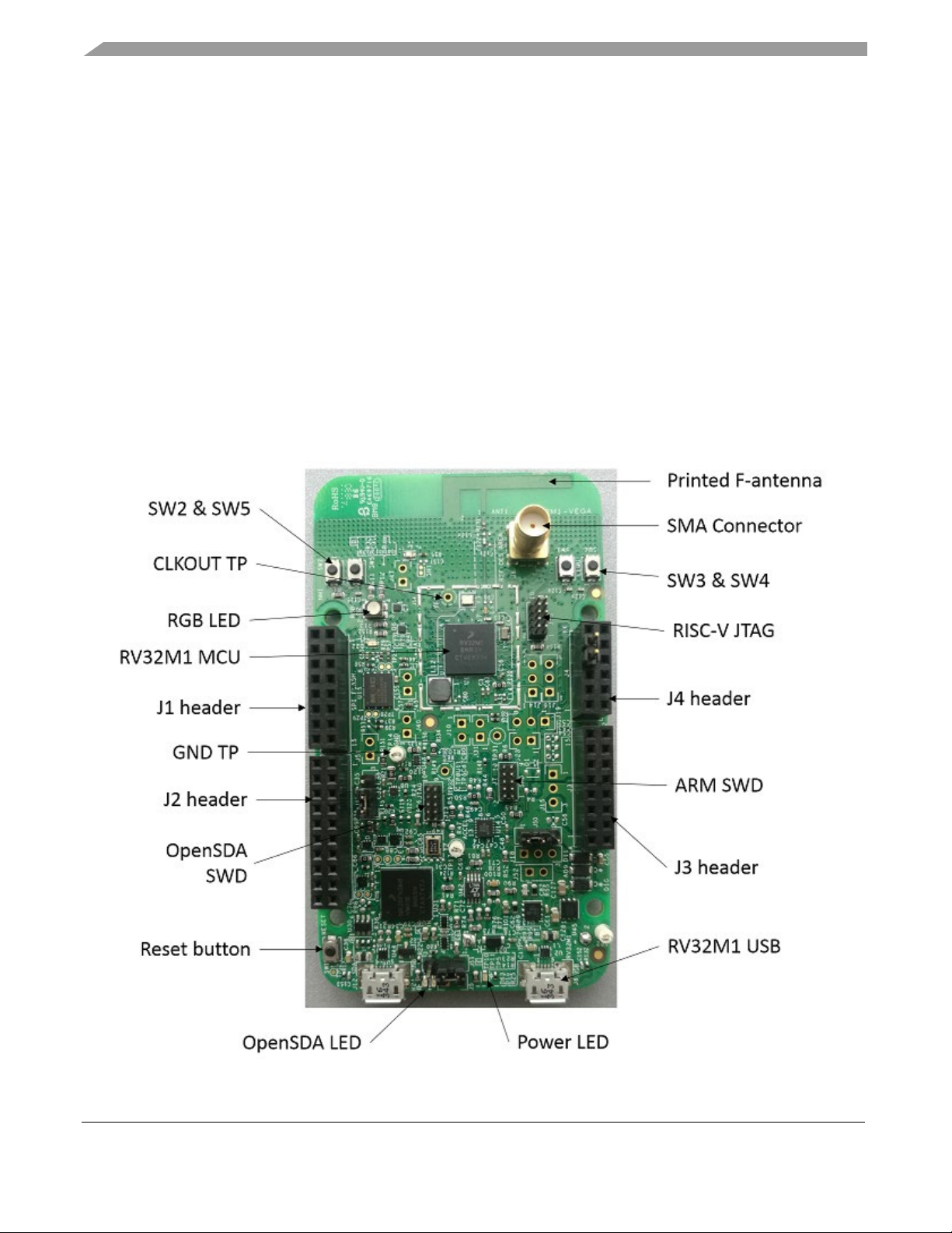
RV32M1-VEGA Development Board
1. Introduction
This guide describes the hardware for the RV32M1-
VEGA Development Board. The RV32M1-VEGA
development board is a small, low-power, and cost-
effective evaluation and development board for application
prototyping and demonstration of the RV32M1 device.
These evaluation boards offer easy-to-use mass-storage-
device mode flash programmer, a virtual serial port, and
standard programming and run-control capabilities.
The RV32M1 is an ultra-low power, highly integrated
single-chip device that enables Bluetooth Low Energy
(BLE), Generic FSK (at 250, 500, 1000 and 2000 kbps) or
IEEE Standard 802.15.4 with Thread support for portable,
extremely low-power embedded systems.
The RV32M1 integrates a radio transceiver operating in
the 2.36 GHz to 2.48 GHz range supporting a range of
FSK/GFSK and O-QPSK modulations, an ARM Cortex-
M4 CPU, ARM Cortex-M0+ CPU, RISC-V RI5CY CPU,
RISC-V ZERO_RISCY CPU, 1.25 MB Flash and 384 KB
SRAM, BLE Link Layer hardware, 802.15.4 packet
processor hardware and peripherals optimized to meet the
requirements of the target applications.
RM32M1-
1. Introduction ........................................................................1
2Overview and description...................................................2
2.1 Overview .................................................................2
2.2 Feature description ..................................................3
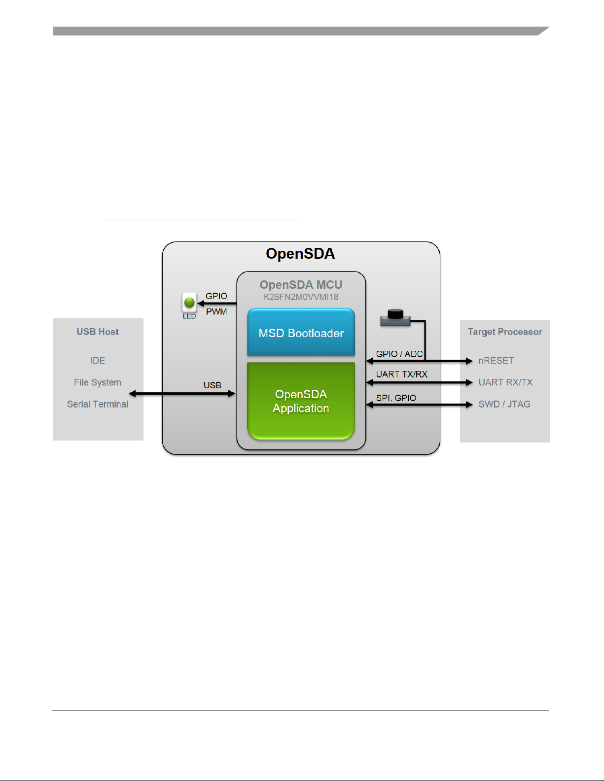
2.3 OpenSDA serial and debug .....................................5
3Functional description ........................................................6
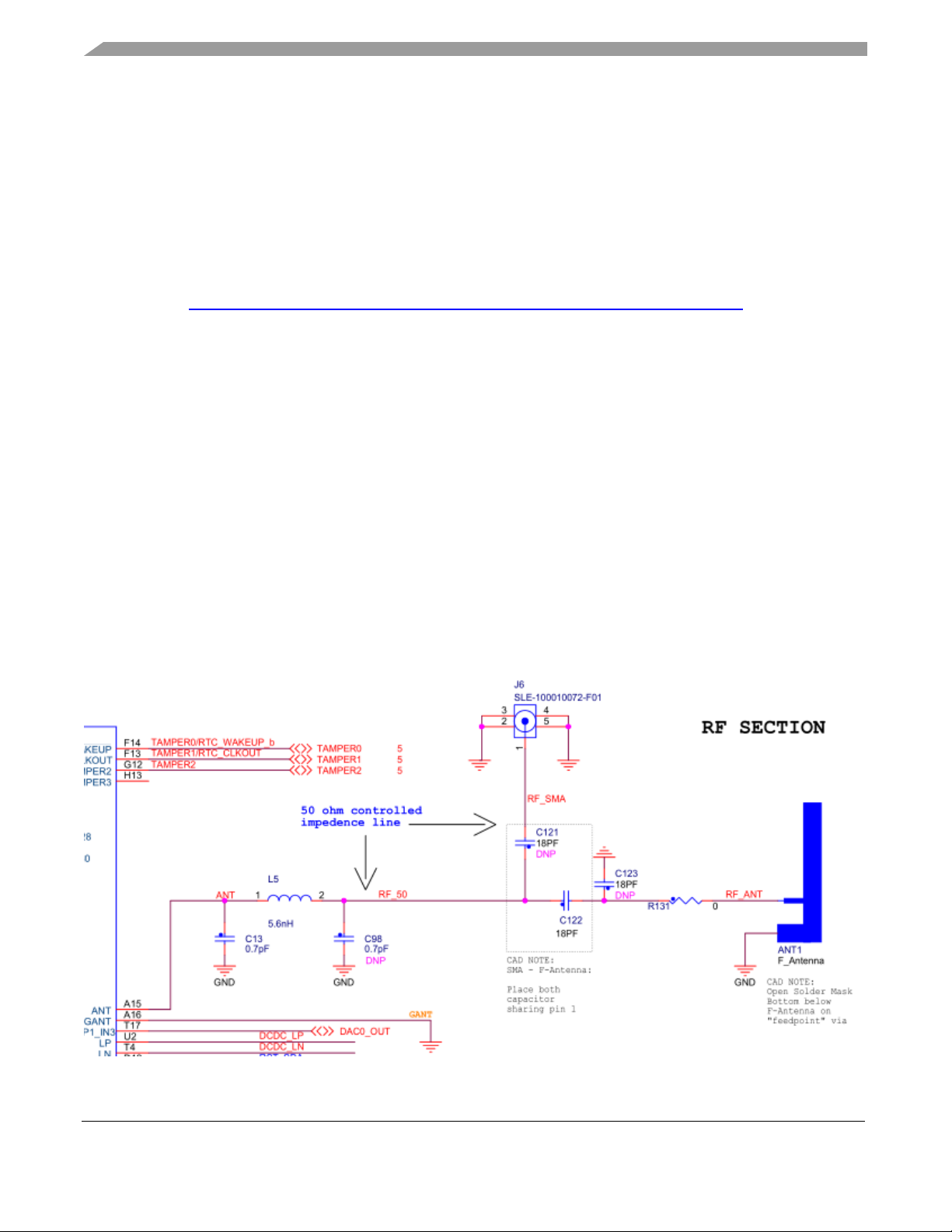
3.1 RF circuit.................................................................6
3.2 Clocks......................................................................7
3.3 Power management .................................................7
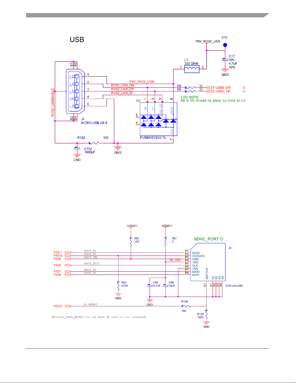
3.4 Universal Serial Bus (USB).....................................8
3.5 Secure Digital Host Controller (SDHC) ..................9
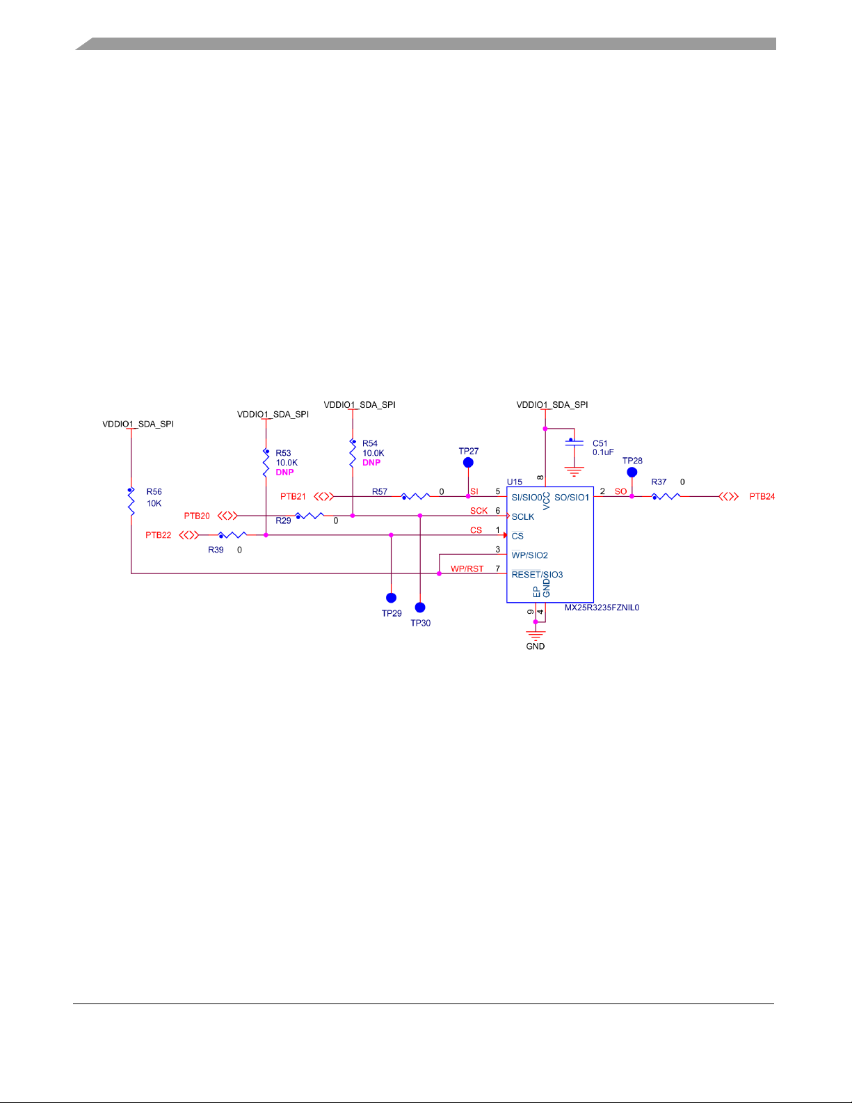
3.6Serial flash memory...............................................10
3.7 Accelerometer + Magnetometer Combo Sensor....10
3.8 Visible light sensor................................................11
3.9 User application LEDs ..........................................12
3.10 User buttons...........................................................12
4Headers and jumpers ........................................................14
4.1 Arduino compatible I/O headers............................14
4.2 Jumper table ..........................................................21
5References ........................................................................22
6Revision history................................................................23