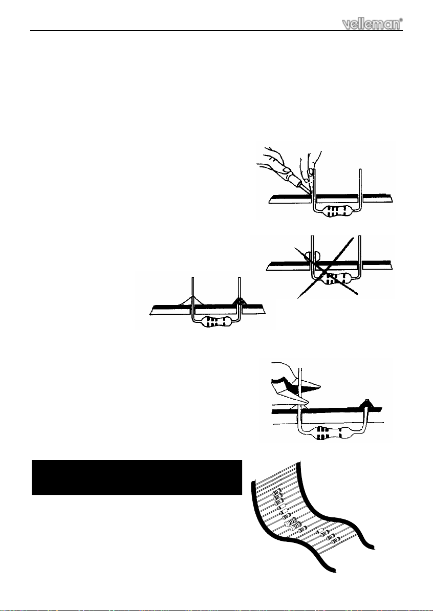
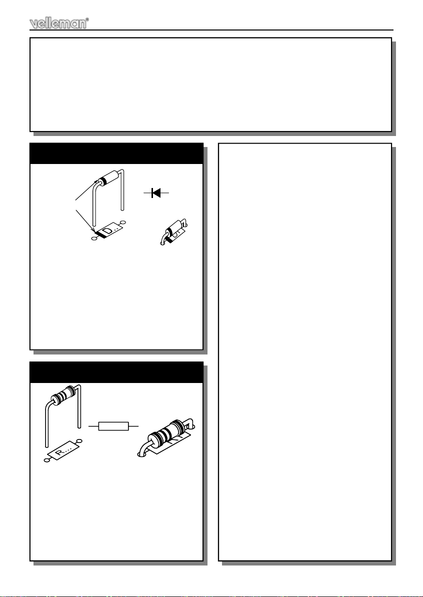
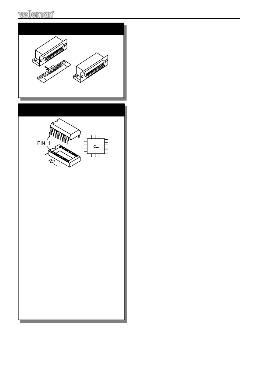
Velleman-Kit K8031 User manual

Total solder points: 625
Difficulty level: beginner 1 234 5 ⌧advanced
DIGITAL PC SCOPE
ILLUSTRATED ASSEMBLY MANUAL H8031P-1
K8031
K8031
Digitalstorageoscilloscoop,usingacomputer
anditsmonitortodisplaywaveforms.All
standardoscilloscopefunctionsareavailablein
theWindowsprogramsupplied.

2
Features & specifications
Features :
1 channel
input impedance: 1Mohm / 30pF
frequency response: 0Hz to 12MHz (± 3dB)
step markers for voltage, time and frequency
vertical resolution: 8 bit
auto setup function
optically isolated from computer
record and display of screens & data
supply voltage: 9 - 10Vdc / 500mA
dimensions: 230 x 165 x 45mm (9" x 6.5" x 1.8")
weight: 400g (14oz)
Minimum system requirements:
• IBM compatible PC
• Windows 95, 98, ME, (Win2000 or NT possible)
• SVGA display card (min. 800x600)
• mouse
• free printer port LPT1, LPT2 or LPT3
• CD Rom player
Specifications
oscilloscope:
• timebase: 0.1µs to 100ms per division
• trigger source: CH1 or free run
• trigger level: adjustable per ½ division
• input sensitivity: 10mV to 3V per division
• record length: 4079 samples
• sampling frequency: 800Hz to 32MHz (Real time)
• true RMS readout (only AC component)
transient recorder:
• timescale: 20ms/div to 2000s/div
• max record time: 9.4hour/screen
• automatic storage of data
• automatic recording for more than 1 year
• markers for time and amplitude
• zoom function
spectrum analyser:
• frequency range: 0 .. 400Hz to 16MHz
• linear or logarithmic timescale
• zoom function

3
Assembly hints
1. Assembly (Skipping this can lead to troubles ! )
Ok, so we have your attention. These hints will help you to make this project
successful. Read them carefully.
1.1 Make sure you have the right tools:
• A good quality soldering iron (25-40W) with a
small tip.
• Wipe it often on a wet sponge or cloth, to keep it clean; then apply solder to
the tip, to give it a wet look. This is called ‘thinning’ and will protect
the tip, and enables you to make good connections. When solder
rolls off the tip, it needs cleaning.
• Thin raisin-core solder. Do not use any flux or grease.
• A diagonal cutter to trim excess wires. To avoid injury when cutting
excess leads, hold the lead so they cannot fly towards the eyes.
• Needle nose pliers, for bending leads, or to hold compo-
nents in place.
• Small blade and Phillips screwdrivers. A basic range
is fine.
For some projects, a basic multi-meter is required, or might
be handy
1.2 Assembly Hints :
⇒ Make sure the skill level matches your experience, to avoid disappointments.
⇒ Follow the instructions carefully. Read and understand the entire step before
you perform each operation.
⇒ Perform the assembly in the correct order as stated in this manual
⇒ Position all parts on the PCB (Printed Circuit Board) as shown on the draw-
ings.
⇒ Values on the circuit diagram are subject to changes.
⇒ Values in this assembly guide are correct*
0.000

4
⇒ Use the check-boxes to mark your progress.
⇒ Please read the included information on safety and customer service
* Typographical inaccuracies excluded. Always look for possible last minute
manual updates, indicated as ‘NOTE’ on a separate leaflet.
1.3 Soldering Hints :
1- Mount the component against the PCB sur-
face and carefully solder the leads
2- Make sure the solder joints are cone-shaped
and shiny
3- Trim excess leads as close as possible to the
solder joint
REMOVE THEM FROM THE TAPE ONE AT A
TIME !
Assembly hints
AXIAL COMPONENTS ARE TAPED IN
THE CORRECT MOUNTING SEQUENCE !

5
Construction
The unit consists out of one main PCB with all the components
Tip: The pictures on the packaging can be used as a guideline.
However, due to possible changes it is not 100% reliable.
Mount the components in the order described:
1. Diodes (check the polarity)
CATHODE
D...
R1 : 150R (1-5-1)
R2 : 470R (4-7-1)
R3 : 150R (1-5-1)
R4 : 47R (4-7-0)
R5 : 150R (1-5-1)
R6 : 91K (9-1-0-2) 1%
R7 : 10K (1-0-3) 1%
2. Resistors (check the color code)
R...
D1: BAS45A
D2: BAS45A
D3: 1N4148
D4: 1N4148
D5: 1N4148
D6: 1N4148
D7: 1N4148
D8: 1N4148
D9 : 1N4148
D10: 1N4148
D11: 1N4148
D12: 1N4148
D13: 1N4148
D14: 1N4148
D15: 1N4148
D16: 1N4007
R8 : 91K (9-1-0-2) 1%
R9 : 3R3 (3-3)
R10 : 910K (9-1-0-3) 1%
R11 : 820R (8-2-0-0) 1%
R12 : 2K2 (2-2-2)
R13 : 820R (8-2-0-0) 1%
R14 : 820R (8-2-0-0) 1%
R15 : 820R (8-2-0-0) 1%
R16 : 1K8 (1-8-2)
R17 : 2K2 (2-2-2)
R18 : 820R (8-2-0-0) 1%
R19 : 10K (1-0-3) 1%
R20 : 10K (1-0-3) 1%
R21 : 10K (1-0-3) 1%
R22 : 10K (1-0-3) 1%
R23 : 10K (1-0-3) 1%
R24 : 10K (1-0-3) 1%
R25 : 10K (1-0-3) 1%
R26 : 20K (2-0-0-2) 1%
R27 : 20K (2-0-0-2) 1%
R28 : 20K (2-0-0-2) 1%
R29 : 20K (2-0-0-2) 1%
R30 : 20K (2-0-0-2) 1%
R31 : 20K (2-0-0-2) 1%
R32 : 20K (2-0-0-2) 1%
R33 : 20K (2-0-0-2) 1%
R34 : 20K (2-0-0-2) 1%
R35 : 470R (4-7-1)
R36 : 2K2 (2-2-2)
R37 : 2K2 (2-2-2)
R38 : 2K2 (2-2-2)
R39 : 100R (1-0-1)
R40 : 150R (1-5-1)
R41 : 2K2 (2-2-2)
R42 : 2K2 (2-2-2)
R43 : 10K (1-0-0-2)1%

6
Construction
C1 : 100n (104, 0.1, u1)
C3 : 100n (104, 0.1, u1)
C6 : 100n (104, 0.1, u1)
C8 : 100n (104, 0.1, u1)
C9 : 100n (104, 0.1, u1)
C12 : 100n (104, 0.1, u1)
C13 : 100n (104, 0.1, u1)
C18 : 100n (104, 0.1, u1)
C19 : 100n (104, 0.1, u1)
C21 : 100n (104, 0.1, u1)
C24 : 100n (104, 0.1, u1)
C25 : 100n (104, 0.1, u1)
C27 : 100n (104, 0.1, u1)
C28 : 100n (104, 0.1, u1)
C29 : 100n (104, 0.1, u1)
C30 : 100n (104, 0.1, u1)
C31 : 100n (104, 0.1, u1)
C32 : 100n (104, 0.1, u1)
C33 : 100n (104, 0.1, u1)
C34 : 100n (104, 0.1, u1)
C36 : 100n (104, 0.1, u1)
C38 : 100n (104, 0.1, u1)
C39 : 100n (104, 0.1, u1)
C40 : 100n (104, 0.1, u1)
C41 : 100n (104, 0.1, u1)
C45 : 100n (104, 0.1, u1)
3. Capacitors
c...
5. IC sockets
C17 : 100p (101)
C26 : 100p (101)
C10 : 220p (221)
C15 : 22p
C16 : 22p
C22 : 22p
C42 : 22p
C4 : 2n2 /100V (222, 2200)
C20 : 2n2 / 100V (222, 2200)
C14 : 2n7 (272, 2700)
C5 : 47n/250V (0.047, 473)
4. Capacitors
C...
IC1: 16P
IC3: 8P
IC4: 24P
IC5: 28P
IC6: 16P
IC7: 16P
IC8: 16P
IC9: 16P
IC10: 16P
IC11: 16P
IC12: 16P
IC13: 24P
IC16: 14P
IC17: 16P
IC18: 8P
IC19: 8P
IC20: 8P
IC21: 8P
IC14: 16P
IC22: 8P
R44 : 2K2 (2-2-2)
R45 : 820R (8-2-0-0) 1%
R46 : 1K8 (1-8-2)
R47 : 100R (1-0-1)
R48 : 100R (1-0-1)
R49 : 100R (1-0-1)
R50 : 470R (4-7-1)
R51 : 470R (4-7-1)
R52 : 470R (4-7-1)
R53 : 3R3 (3-3) / 1W
C47 : 100n (104, 0.1, u1)
C48 : 100n (104, 0.1, u1)

7
Construction
C2 : 4µ7
C7 : 4µ7
C11 : 4µ7
C35 : 4µ7
C37 : 4µ7
C44 : 4µ7
C23 : 100µF
C43 : 100µF
C46 : 100µF
6. Electrolytic capacitors. Check
the polarity !
C...
T1 : BC327
7. Transistor
RV1: 50R (R50, W500)
RV2: 500R (R500, W501)
In doubt, measure using an ohm meter
between the two outer connections.
8. Multiturn trimmer
RV...
CV1 : 22p (small type)
CV2 : 50p
9. Trimmer capacitors
CV...
X1: 32MHz
Check the position, refer to the PCB
lay out.
10. Oscillator
X...
FS1: 1A pico
One spare fuse is also supplied
11. Pico fuse
FS...

8
RY1 : VR05R051AS
RY2 : VR05R051AS
RY3 : VR05R051AS
RY4 : VR05R051AS
RY5 : VR05R051AS
12. Reed relays (check the posi-
tion of the notch)
RY...
J4 : PCB tab
This tab serves as square wave out-
put test signal.
13. PCB tab
SK...
J4
IC15 : UA7805
Mount the regulator like in the
drawing.
First fix the regulator, then solder
the connections.
14. Voltage regulator.
M3 NUT
LOCK WASHER
M3 BOLT
J2 : DJ-005
15. DC jack
-
SK... +
SW
LD: 3mm LED
16. Power indication LED, comes
later through the front panel
LD...
CATHODE
3mm
J1 : BNC
Carefully solder the connections.
17. BNC connector
Construction
IMPORTANT
Mount this LED exactly like
in the drawing, otherwise
the LED will not fit correctly
in the front panel.

9
J6 : 25P sub D male
18. 25P sub D connector
R...
5mm
IC1 : 74F161
IC3 : OPA2350PA
IC4 : TDA8703
IC5 : 6264 ; CY7C199.....EQ
IC6 : 74HC153
IC7 : 74F161
IC8 : 74F161
IC9 : 74HC595
IC10 : 74HC85
IC11 : 74HC595
IC12 : 74HC595
IC13 : VK8031 (PAL22V10)
IC14 : 74HC390
IC16 : 74HC14
IC17 : 74HC390
IC18 : 6N136
IC19 : 6N136
IC20 : 6N136
IC21 : 6N136
IC22 : 6N136
19. IC’s check the position !
Construction

10
Construction
Cut the screening foil like in the drawing.
Make sure the conductive side is faced downwards !!
Position the screen foil into the bottom enclosure.
Use some adhesive tape to fix the screen foil
Make sure the conductive side is faced downwards !!
20. Screen foil preparation
Fig. 1.0
80mm
10mm
20mm
Fig. 2.0

11
Construction
© Velleman Kit
IC23: 7805 (UA7805P) - This regulator must be isolated plastic type !
Mount the voltage regulator on the rear panel and fasten it with the supplied M3
bolt, washer and nut as shown on the drawing. Make sure to remove the pro-
tective foil from the front and rear panel!
Assemble the enclosure as following:
Position the PCB together with the front and rear panel in the bottom half of the
enclosure. Fasten the PCB in the enclosure.
Now the voltage regulator can be soldered at the component side of the PCB,
not at the solder side.
Mount a LED clip into the test signal hole (1).
See next page for screen foil fixation and position
21. Voltage regulator and PCB assembly
M3 NUT
M3 LOCK WASHER
VOLTAGE REGULATOR
M3 BOLT
Fig. 1.0
Fig. 2.0
1

12
Construction
Make sure the conductive side is faced downwards !
Fix the screen foil using a washer and screw. (Push the screw through the foil)
The conductive side must make contact with the PCB surface.
* Please note that you should tape both front and back of the three visible
edges in order to avoid all contact between the screening foil and the
components.
ATTENTION ! : Make sure that the screening foil does not make any electrical
contact with the front panel while you are fixing the screening foil to the PCB.
22. PCB and screen foil fixation
Fig. 1
Tape*

13
Test & adjustment
• Install the PC-Lab2000 software (see getting started manual)
• Connect the unit using a parallel cable to the computer LPT port.
• Connect a 9V/500mA power supply to the unit. (check the polarity). The LED
on the front panel should lid.
• Start the PC-Lab2000 software and select K8031 hardware and the appropri-
ate port.
• Short circuit the input using an appropriate probe or connection.
• Press the RUN button.
For all adjustment select DC input and Trigger off
Offset adjustment:
• Make sure that the Y position slider is in the centre position
• Switch always between 1V/div and 3V/div setting
• Adjust RV1 until the signal remains stable in the centre of the screen
Transient adjustment and calibration:
• Select 1V/div
• Connect the input to test point J4
• Adjust CV1 until the signal top is as flat as possible
• In the VIEW menu select “RMS value”
• Adjust RV2 until the signal is 2.5Vrms
• Select 0.3V/div
• Connect the input to test point J3
• Using the Y position slider set the signal in the centre of the screen
• Adjust CV2 until the signal top is as flat as possible
Repeat the transient adjustment and calibration at least once.
Finally use the calibrate and exit option in the File menu to complete the calibration.
Mount the cover onto the enclosure (fold the screen foil).
The unit is now ready for use. Check the CD for more information.
23. Test and adjustment
NG OK NG
Fig. 1

14
PCB
24. PCB

15
25. Digital selection
Schematic diagram

16
© Velleman Kit Values are for reference only
26. Opto Coupler selection
Opto coupler selection

17
© Velleman Kit Values are for reference only
27. Input selection
Input selection

18
Note :

19
Note :

VELLEMAN KIT NV
Legen Heirweg 33
9890 Gavere
Belgium Europe
Info ?: http://www.velleman.be
Modifications and typographical errors reserved
© Velleman Kit nv
H8031IP - 2003 - ED1
5410329 291044
Other Velleman-Kit Test Equipment manuals
Popular Test Equipment manuals by other brands

Levenhuk
Levenhuk ERMENRICH ZING WT40 user manual

Dwyer Instruments
Dwyer Instruments CSG user guide

Launch
Launch Creader CR3001 quick start guide

yellow jacket
yellow jacket 67060 quick start guide

Sperry instruments
Sperry instruments ET6207 operating instructions

Keysight Technologies
Keysight Technologies 85033E User and service manual