Virginia Diodes ZBD Quick start guide

979 Second Street SE, Suite 309
Charlottesville, VA 22902-6172 (USA)
Tel: 434.297.3257; Fax: 434.297.3258
www.vadiodes.com
© 2020 Virginia Diodes, Inc –All Rights Reserved
Zero-Bias Detector Operational Manual
(ZBD, ZBD-F, QOD)
2020

2
© 2020 Virginia Diodes, Inc.—All Rights Reserved—Rev: 12 June 2020
Section 1 –ZBD General Overview, Safety and Operational Guidelines........Pages 2-3
Contents.....................................................................................................................................................Page 2
ZBD General Overview, Safety and Operational Guidelines .....................................................................Page 3
Section 2 –Product Overview and Specifications ..................................................Pages 4-7
Product Overview....................................................................................................................................Page 4-5
Configurations (ZBD vs. ZBD-F) ................................................................................................................Page 6
Product Specifications................................................................................................................................Page 7
Appendix 1 –ZBD Responsivity Performance..........................................................Pages 8-9
ZBD Performance –WR10 and WR6.5 ....................................................................................................Page 8
ZBD Performance –WR5.1 and WR2.2 ....................................................................................................Page 9
Appendix 2 –Responsivity vs. RF Input Power..........................................................Pages 10
Responsivity vs. RF Input Power ............................................................................................................Page 10
Appendix 3 –IF Amplifier Pre-testing before use with VDI Detector.................Pages 11
Amplifier Pre-testing before use with VDI Detector .................................................................................Page 11
Addendum –Product Updates and Company Contacts ...........................................Page 12
Contents
Section
One

3
© 2020 Virginia Diodes, Inc.—All Rights Reserved—Rev: 12 June 2020
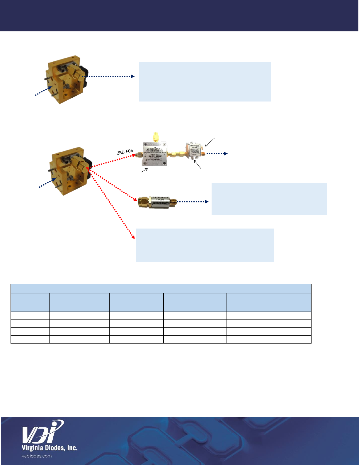
Zero-Bias Detectors (ZBD)
Virginia Diodes offers zero biased, Schottky diode detectors for a variety of millimeter wave and
terahertz applications. These detectors provide high responsivity and extremely fast response time. VDI
detectors offer full waveguide band coverage and are available from WR15 (50-75 GHz) to WR0.65
(1100-1700 GHz). Higher frequency custom detectors are available upon request.
Safety and Operational Guidelines
Read all instructions and information in this product manual before connecting the product to external equipment.
Operational procedures must be followed for proper function. If you have questions, contact VDI before operating the
product.
The internal components of every detector can be damaged by Electro Static Discharge (ESD). Any operator using or
handling the device should wear a grounded wrist strap specifically designed to guard against ESD. The work
environment including test benches should also be properly grounded.
VDI assumes the customer is familiar with microwave, millimeter wave, and VDI products in general. The user and
customer are expected to understand all safety guidelines, health hazards, and general advisories that may exist and
are associated with the use of this device. VDI is not responsible for any human hazards that may exist or may occur
while using this device.
Virginia Diodes, Inc. (VDI) accepts no liability for damage or injury resulting from or caused by:
•Improper use, disassembly or use for purposes other than those for which the product was designed;
•Use outside common safety, health or general advisories pertaining to microwave, millimeter wave, and VDI products;
•Repairs carried out by persons other than VDI or its assigned agents.
Waveguide Inspection / Test Port Care
•Inspect waveguide flanges for debris prior to making connections.
•Making a connection with metal debris between the waveguide flanges can damage the waveguide interface and prevent
repeatable connections.
•If debris is present, clean the flange with pre-dampened lint free wipes or swabs (e.g. TexWipe TX1065). If these are not
available, lint free cloths lightly dampened with ethanol may be used (e.g. TexWipe TX604).
•When device is not in use, cover appropriate waveguide flanges with provided dust cap or protective waveguide tape.
•Waveguide screws should be torqued between 20-50 cNm, greater values can damage the interface.
•Use a torque of 90 cNm when making coaxial connections. Avoid sharp bends in cables.
General Operating Practices and Recommendations
•Check with VDI before any use is attempted beyond those described in this manual, including uses that may exceed
limitations stated here or commonly accepted standards of practice.
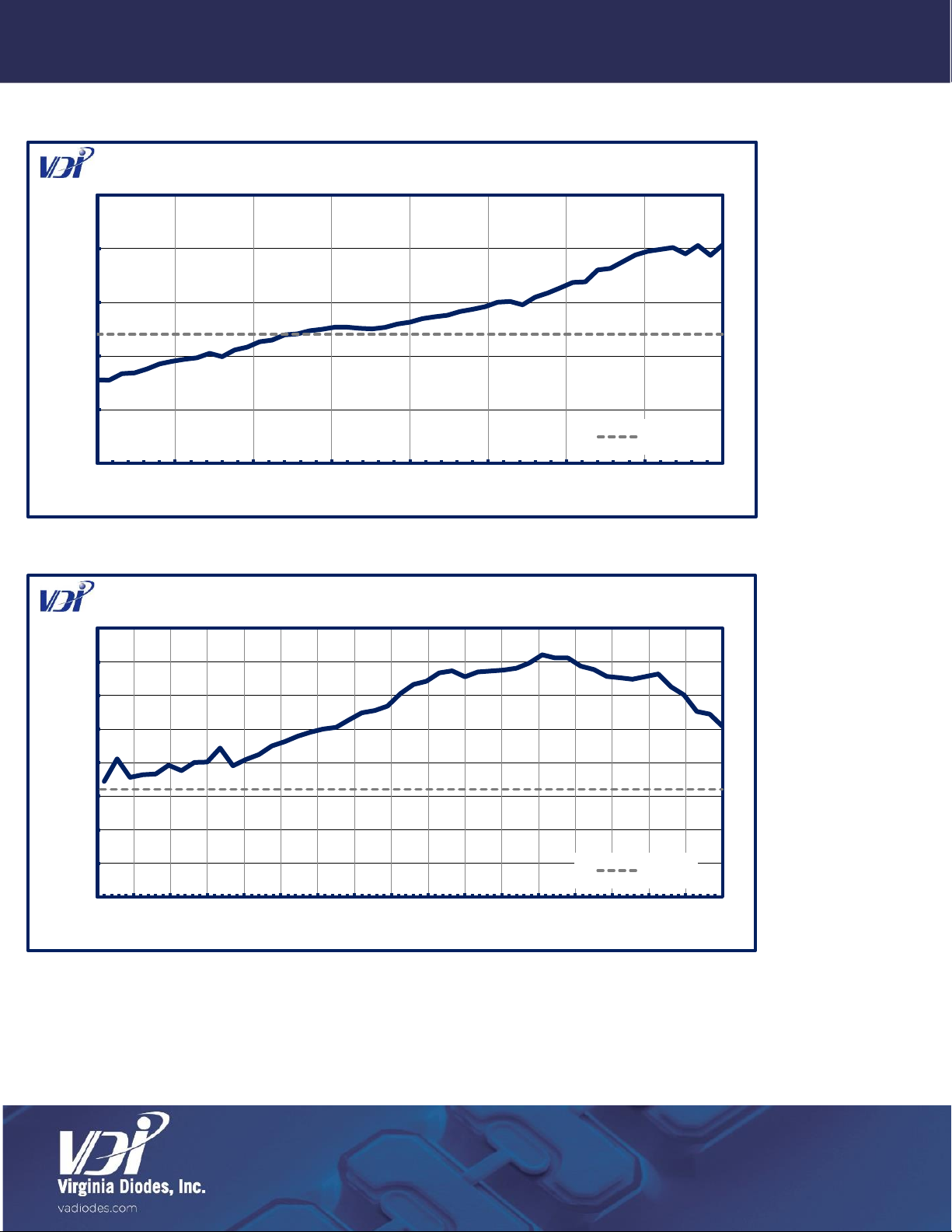
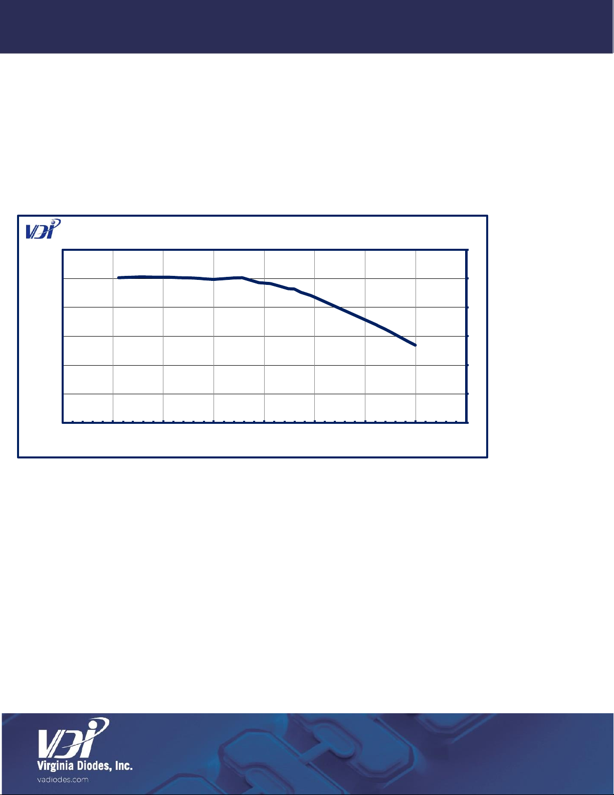
•Specifications listed in this document reflect the latest specifications. For ZBDs shipped prior to July 3, 2019, please refer
to individualized data sheets.
ZBD General Overview, Safety and Operational Guidelines

4
© 2020 Virginia Diodes, Inc.—All Rights Reserved—Rev: 12 June 2020
Low Frequency Zero Bias Detectors (WR-15 to WR-10)
These detectors have a rectangular waveguide RF input port and coaxial output. The drawings and corresponding dimensions are for a typical WR-10 and WR-15
zero bias detector. The WR12ZBDs have similar form factor to the WR15ZBD.
Middle Frequency Zero Bias Detectors (WR-8.0 to WR-1.0)
These detectors have a rectangular waveguide RF input port and coaxial output. The drawings and corresponding dimensions are for typical WR-3.4 zero bias
detectors. Other ZBDs (WR-8.0 to WR-1.0) have similar configuration and dimensions.
High Frequency Zero Bias Detectors (WR-0.8 to WR-0.65)
The WR0.8ZBD has an integrated horn antenna (~25dBi) RF input port and a coaxial output. The WR0.65ZBD has a rectangular waveguide RF input port and a
coaxial output. The drawing and corresponding dimensions are for a typical WR-0.65 and WR-0.8 zero bias detector.
Section
Two
Product Overview
WR-10
RF Input Port
E-Field
Output
0.80”
1.50”
1.30”
RF Input Port
E-Field
Output
0.80”
1.50”
1.20”
WR-15
WR-3.4
RF Input Port
E-Field
Output
0.80”
1.25”
0.80”
WR-0.8
0.80”
1.25”
0.80”
RF Input Port
E-Field
Output
WR-0.65
0.80”
1.50”
0.65”
E-Field
Output
RF Input Port

5
© 2020 Virginia Diodes, Inc.—All Rights Reserved—Rev: 12 June 2020
Quasi-Optical Detectors (QOD)
The photograph for a typical quasi-optical detector (~1.50” x 1.50” x 0.45”) is shown below. These detectors will have a silicon lens RF input port and a coaxial
output port. The E-Field polarization will change with frequency (±22.5°). The polarizations shown below are nominal polarizations. The QOD alignment should be
adjusted for optimal performance. VDI includes RF absorber around the silicon lens with every QOD. VDI recommends the use of RF absorber around the silicon
lens to reduce reflections and potential standing waves.
General Operating Procedure
These procedures apply to all VDI zero-bias detectors.
Turn On: Apply small signal RF input power and monitor detector output response.
Turn Off: Turn off small signal input power.
RF Input Port: DO NOT exceed damage limits listed on Page 7.
Output Port (Extremely ESD Sensitive): The detector output port is extremely ESD sensitive. DO NOT apply any DC biases or surges when connecting /
disconnecting from output port. Discharge static from cables before connecting to the device. Replace IF port with provided 50Ωtermination or appropriate cover
when output port is not in use.
ZBD (Internal ESD Protection Circuit): Monitor detector output port using a floating voltmeter. See Page 6 for configuration details.
ZBD-F Configuration (using Bias-Tee and Amplifier): Appropriate voltages must be applied to the voltage pins on the provided amplifier.
ZBD-F Configuration (using External ESD Protection Circuit): Monitor detector output port using a floating voltmeter. See Page 6 for configuration details.
Black Backing Plate: Unused ports are covered by a black backing plate. DO NOT tamper with the black backing plate.
Failure to follow these procedures may damage or destroy the device. The user is liable for repair costs of detectors damaged by ESD, and the use of stringent
ESD precautions is recommended when making connections to VDI detectors.
Replacing Bias-Tee / Amplifier with External ESD Protection Circuit (ZBD-F only)
These procedures apply to ZBD-F configurations only.
An External ESD Protection Circuit is included (detached) and can be used for applications where a low frequency (DC to ~50kHz) detector output is more
appropriate. To use the External ESD Protection Circuit, the bias-tee and amplifier must be removed and then connect the External ESD Protection Circuit can be
connected to the detector output port. When there is nothing attached to the detector output port, the detector can be damaged by ESD events. Please use safe
ESD guidelines when disconnecting and connecting components from the detector output port.
E-Field
Output
RF Input Port
Product Overview –Continued
H-Field

6
© 2020 Virginia Diodes, Inc.—All Rights Reserved—Rev: 12 June 2020
ZBD (Internal ESD Protection)
Standard ZBD configuration
ZBD-F (Fast Detector)†
Standard ZBD-F configuration includes 6 GHz bias-tee and amplifier.
Fast Detector Technical Notes:
*Fast Detectors are shipped with a 6 GHz bias-tee and amplifier attached to the detector unless other options are specified. Additional fast detector options are
shown in the table above and can be purchased at an additional cost. Contact VDI for more information.
*Amplifiers included in the F06, F20, and F40 options have a 50 ohm input impedance. The amplifier included in the FDA option has a high input impedance. The
total gain or loss through the ZBD-F (detector, bias-tee and amplifier) will depend on the output impedance of the ZBD and the input impedance of the amplifier.
Impedance mismatch will reduce the signal out of the amplifier. The amplifier included in the FDA option is better matched with the ZBD compared to the other
amplifier. Therefore, there will be less signal degradation through the amplifier included in the FDA option compared to the other amplifiers.
*Amplifier gain performance assumes correct testing conditions (bias voltage, input impedance, output impedance) specified in the above table.
Fast Detector Options
Fast
Detector
Option
Frequency Range
Gain (dB, typical)
Bias Voltage
Input
Impedance
Output
Impedance
ZBD-FDA
~2 kHz to 40 MHz
40
+5 V (~50mA)
High Impedance
50 Ω
ZBD-F06
~50 MHz to 6 GHz
15
+5V (~80mA)
50 Ω
50 Ω
ZBD-F20
~ 100 MHz to 20 GHz
12
+12V / -5V (~80mA)
50 Ω
50 Ω
ZBD-F40
~50 MHz to 40 GHz
10
+5 V (~100mA)
50 Ω
50 Ω
Configurations (ZBD vs. ZBD-F)
External ESD Protection Circuit Output:
DC to ~250 kHz
~0.5-1kΩ Output Impedance
Provides ESD Protection
Output:
DC to ~250 kHz
~3-6kΩ Output Impedance
No access to full detector response rate
Provides ESD Protection
External components can be removed to access
full detector frequency response rate.
Detector Output Port Extremely ESD Sensitive
See Maximum Detector Response Rate on Page 7
RF Input
RF Input
DC Bias Connections
Amplifier
Bias-Tee
Output
External ESD Protection Circuit

7
© 2020 Virginia Diodes, Inc.—All Rights Reserved—Rev: 12 June 2020
†Diagonal Horn antenna has a gain of ~25dBi, specified at the middle of the waveguide band. The gain changes as a function of frequency. See VDI Application Note: VDI
Waveguide Feedhorn Specification (VDI-1001) for more information.
‡ Output Lens Directivity: 25-35dB nominal.
*Typical Responsivity assumes ZBD is operated in the linear region, before saturation. Responsivity may be reduced toward band edges.
**Maximum Response Rate applies to the bare ZBD housing; additional components such as ESD protection, bias tees, and amplifiers may further limit the response rate.
Part Number Format
Use “VDI Part Number” in above table (ZBD or QOD) with appropriate suffix; -FXX = Fast Detection option with bias tee / amplifier
XX = 06, 20 or 40 (if 6, 20 or 40 GHz Bias-Tee / Amplifier Option is chosen)
Examples:
WR8.0ZBD: 90-140 GHz Zero-Bias Detector with Internal ESD Protection Option
WR8.0ZBD-F06: 90-140 GHz Fast Detector with 6 GHz Bias-Tee / Amplifier Option (attached) and External ESD Protection Circuit (detached)
WR8.0ZBD-F20: 90-140 GHz Fast Detector with 20 GHz Bias-Tee / Amplifier Option (attached) and External ESD Protection Circuit (detached)
QOD-F40: Quasi-Optical Detector (100-1000 GHz) Fast Detector with 40 GHz Bias-Tee / Amplifier Option (attached) and External ESD Protection Circuit (detached)
General Specifications for Zero-Bias Detectors
Description
Specification
Detector Output Flange
ZBD (with Internal ESD Protection)
2.9mm(f)
ZBD-F (with Bias Tee and Amplifier)
2.9mm(f)
ZBD-F (with External ESD Protection)
2.9mm(f)
RF Input Power
Linear (typ.)
< -25 dBm
1dB Compression (typ.)
-20 dBm
Maximum RF Input Power
(for ZBDs only)
Recommended / Damage (for WR15 to WR2.8)
0 dBm / 5 dBm
Recommended / Damage (for all other ZBDs)
-3 dBm / 0 dBm
Maximum RF Input Power
(for ZBD-Fs only)
Recommended / Damage (for WR0.65 only)
-3 dBm / 0 dBm
Recommended / Damage (for all other ZBD-Fs)
0 dBm / 5 dBm
Maximum Weight (ZBD / ZBD-F)
~0.1lbs. / ~0.3 lbs.
Operating Temperature (Typical / Recommended)
25°C / 20-30°C
Product Specifications for Zero-Bias Detectors
VDI Part
Number
RF
Frequency
(GHz)
RF Input Flange
Typical
Responsivity (V/W)*
Typical NEP
(pW/√Hz)
Maximum
Response
Rate (GHz)**
ZBD
ZBD-F
ZBD
ZBD-F
WR15ZBD
50-75
WR-15 UG-385/U
3000
2400
8.9
1.1
~10
WR12ZBD
60-90
WR-12 UG-387/U-M
2800
2300
9.5
1.1
~12
WR10ZBD
75-110
WR-10.0 UG-387/U-M
2800
2300
9.5
1.1
~15
WR8.0ZBD
90-140
WR-8.0 UG-387/U-M
2400
2300
11.0
1.1
~19
WR6.5ZBD
110-170
WR-6.5 UG-387/U-M
2400
2300
11.0
1.1
~24
WR5.1ZBD
140-220
WR-5.1 UG-387/U-M
2400
2300
11.0
1.1
~31
WR4.3ZBD
170-260
WR-4.3 UG-387/U-M
2400
2000
11.0
1.3
~36
WR3.4ZBD
220-330
WR-3.4 UG-387/U-M
2200
1900
12.0
1.3
~40
WR2.8ZBD
260-400
WR-2.8 UG-387/U-M
1600
1200
16.5
2.1
~40
WR2.2ZBD
330-500
WR-2.2 UG-387/U-M
1600
1200
7.2
2.1
~40
WR1.9ZBD
400-600
WR-1.9 UG-387/U-M
1000
700
11.4
3.5
~40
WR1.5ZBD
500-750
WR-1.5 UG-387/U-M
1000
600
11.4
4.1
~40
WR1.2ZBD
600-900
WR-1.2 UG-387/U-M
750
400
15.2
6.1
~40
WR1.0ZBD
750-1100
WR-1.0 UG-387/U-M
750
300
15.2
8.2
~40
WR0.8ZBD
900-1400
~25dBi Diagonal Horn†
100
100
113.7
24.4
~40
WR0.65ZBD
1100-1700
WM-164 UG-387/U-M
100
100
113.7
113.7
~40
QOD
100-1000
Silicon Lens‡
100-250
80-200
45-115
12-30
~40
Product Specifications

8
© 2020 Virginia Diodes, Inc.—All Rights Reserved—Rev: 12 June 2020
ZBD Responsivity Performance
Typical responsivity plots are provided on the following page. More data is available on the VDI website. The responsivity is
defined as the ratio between the output voltage and the RF input power in the linear region. Measured performance data will be
shipped with each ZBD. Data shown in this manual is for ZBD (not ZBD-F) configurations only.
ZBD Performance –WR10 and WR6.5
Appendix
One
0
1000
2000
3000
4000
5000
6000
75 80 85 90 95 100 105 110
Responsivity (V/W)
Frequency (GHz)
WR10ZBD
Typical
0
1000
2000
3000
4000
5000
6000
110 120 130 140 150 160 170
Responsivity (V/W)
Frequency (GHz)
WR6.5ZBD
Typical

9
© 2020 Virginia Diodes, Inc.—All Rights Reserved—Rev: 12 June 2020
ZBD Performance –WR5.1 and WR2.2
0
1000
2000
3000
4000
5000
140 150 160 170 180 190 200 210 220
Responsivity (V/W)
Frequency (GHz)
WR5.1ZBD
Typical
0
500
1000
1500
2000
2500
3000
3500
4000
330 340 350 360 370 380 390 400 410 420 430 440 450 460 470 480 490 500
Responsivity (V/W)
Frequency (GHz)
WR2.2ZBD
Typical

10
© 2020 Virginia Diodes, Inc.—All Rights Reserved—Rev: 12 June 2020
Responsivity vs. RF Input Power
The plot below is an example of how the responsivity changes as a function of RF input power for a specific WR10 detector at ~93
GHz. For small signal RF input power, the detector is in the square law region, where the detector output voltage is proportional to
the RF input power.
The general shape of the curve is consistent for all diode detectors. However, the scale will vary with frequency and the detector
design and other operating conditions, for example temperature.
Responsivity vs. RF input power data can be supplied for all shipped ZBDs at an additional cost.
Figure 1: Responsivity vs. RF Input Power
The performance (responsivity vs. RF input power) is shown for a specific WR10ZBD at ~93 GHz.
0
500
1000
1500
2000
2500
3000
-45 -40 -35 -30 -25 -20 -15 -10 -5
Responsivity (V/W)
RF Input Power (dBm)
Responsivity vs. RF Input Power
Appendix
Two

11
© 2020 Virginia Diodes, Inc.—All Rights Reserved—Rev: 12 June 2020
Though VDI ZBDs offer extremely wideband performance, they are extremely ESD sensitive at its coaxial detector output port. To
add ESD protection, an amplifier is recommended. However, some amplifiers can exhibit bias or turn-on transients at the amplifier
input, which can damage the VDI ZBD. Even with AC coupling at the amplifier input, transients can occur when the amplifier bias
is applied rapidly.
Before using an amplifier with a VDI detector, it is recommended that bias or turn-on transients at the amplifier input be tested.
Attach a 1kΩresistor to the input of the amplifier. Monitor the resistor voltage on an oscilloscope as the amplifier bias is applied.
The turn-on transient voltages across the resistor should be kept less than ~100mV for safe operation.
Appendix
Three
Amplifier Pre-Testing before Use with VDI Detector
VDI Detector with External Amp
Turn-on Transient Testing
Figure 2: Amplifier Pre-Testing
Block diagrams of amplifier pre-testing, prior to use with VDI detector is shown.

12
© 2020 Virginia Diodes, Inc.—All Rights Reserved—Rev: 12 June 2020
The Virginia Diodes staff of engineering and physical science professionals works to continually improve our products. We also
depend upon feedback from colleagues and customers. Ideas to simplify component operations, improve performance or add
capabilities are always welcome.
Contact VDI:
Virginia Diodes, Inc.
Web: http://www.vadiodes.com
Email: Technical@vadiodes.com
Telephone: 434.297.3257
Addendum —Product Updates and Company Contacts
This manual suits for next models
2
Table of contents
Other Virginia Diodes Measuring Instrument manuals
Popular Measuring Instrument manuals by other brands

Mastech
Mastech MS6900 user manual

Newtons4th
Newtons4th PSM3750 NumetriQ user manual

Sharp
Sharp MD-MT270HS/BK Service manual

PCE Instruments
PCE Instruments PCE-CT 5000 instruction manual

Synthesis Technology
Synthesis Technology E370 Quad Morphing VCO manual

Oldham
Oldham MX15 Installation and operating instructions