Winbond W6810 User manual

WECA W6810DK
2727 N First Street, San Jose CA 95134
1
Winbond W6810 Codec
Evaluation System
User’s Guide
W6810DK Evaluation Board Rev 1.06
查询W6810_1供应商 捷多邦,专业PCB打样工厂,24小时加急出货

WECA W6810DK
2727 N First Street, San Jose CA 95134
2
Chapter - 1...................................................................................................................................................... 3
General Description........................................................................................................................................ 3
Introduction: ................................................................................................................................................... 3
W6810DK Features:....................................................................................................................................... 3
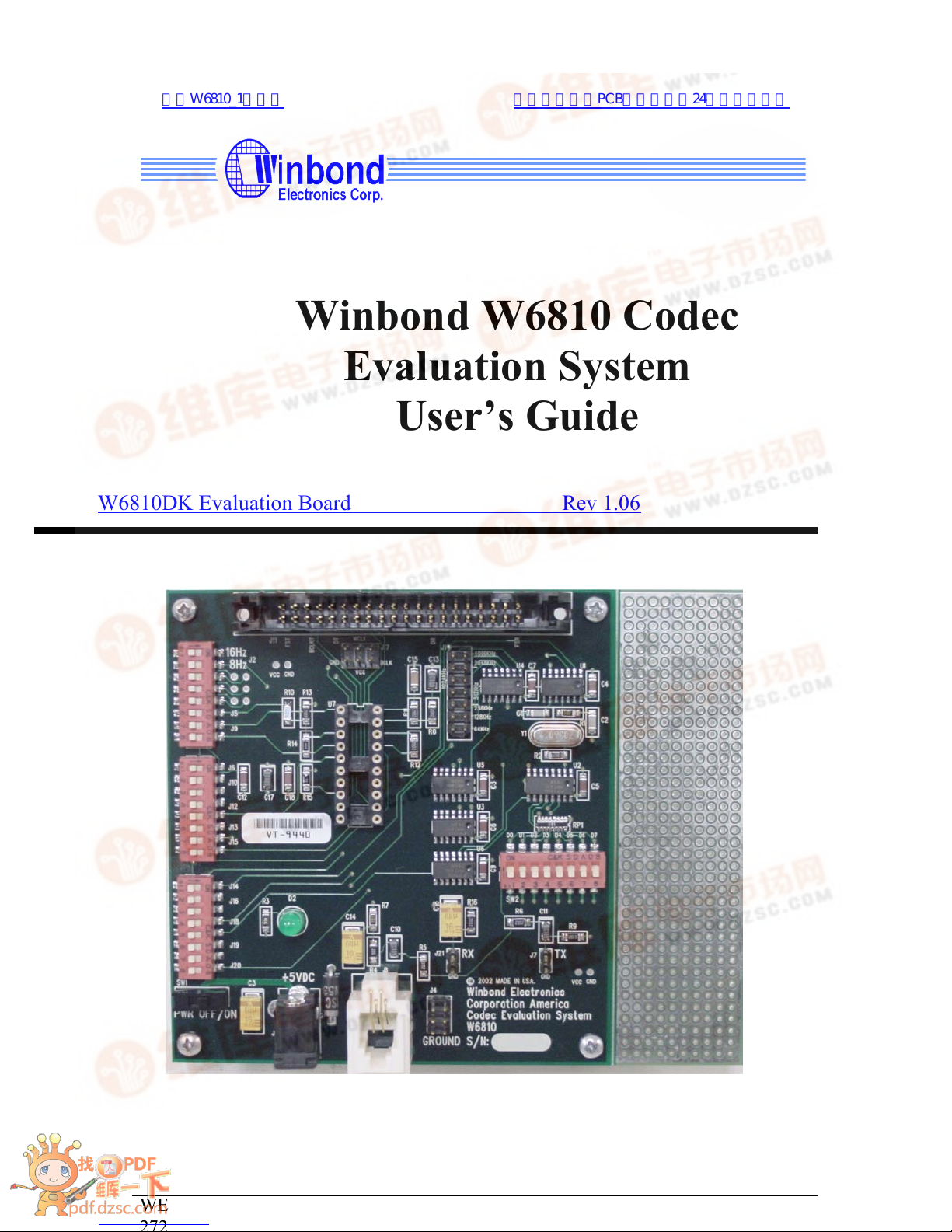
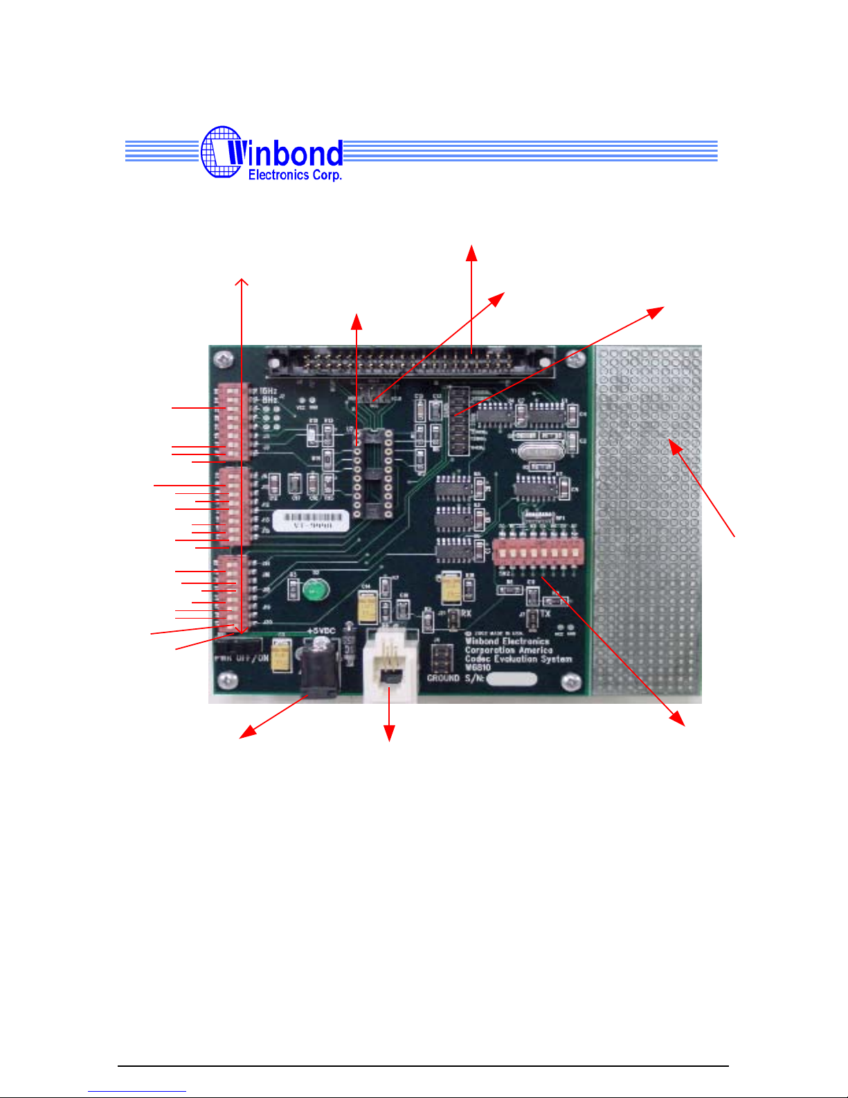
Figure 1: W6810DK Evaluation System Component Placement ............................................................................. 4
Chapter - 2...................................................................................................................................................... 5
Hardware Description..................................................................................................................................... 5
Clock Generator: ............................................................................................................................................ 5
Frame Sync:.................................................................................................................................................... 5
BIT CLOCK:.................................................................................................................................................. 6
256 KHZ:........................................................................................................................................................ 6
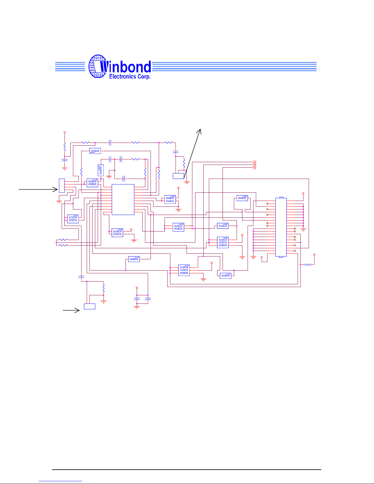
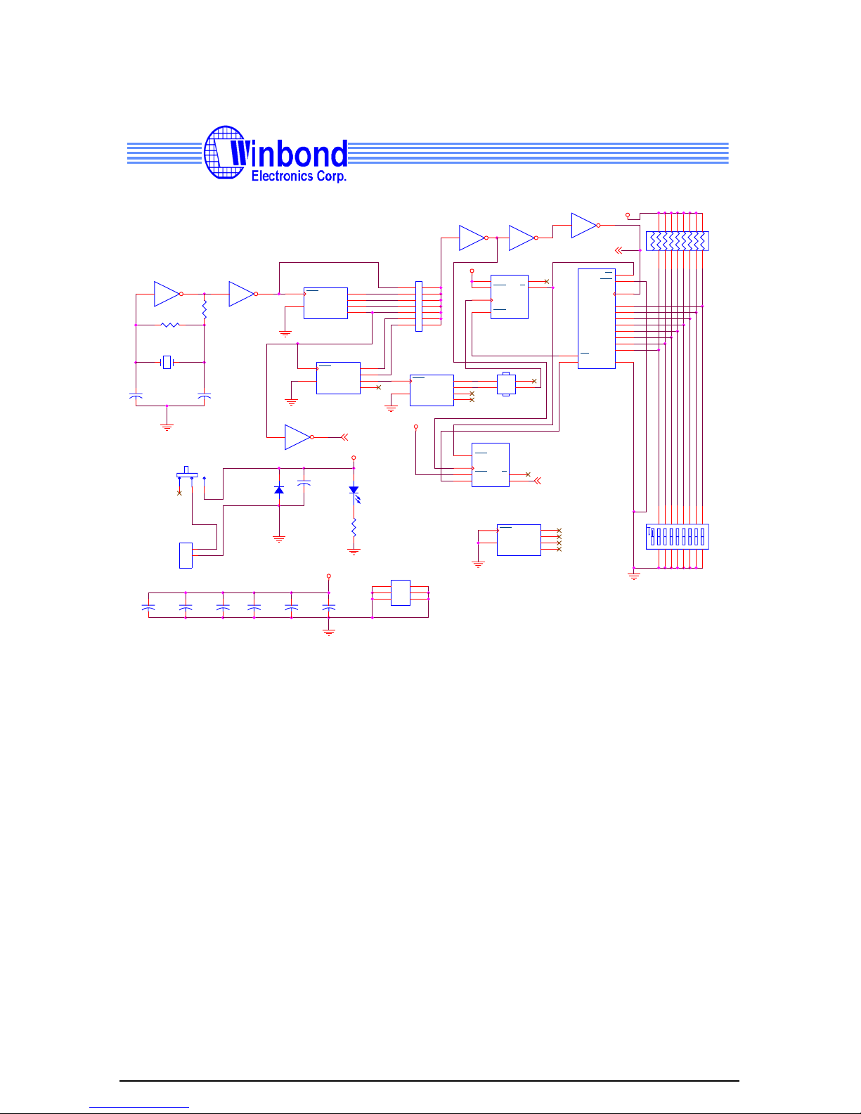
Figure 2: W6810DK Evaluation System Schematics diagram....................................................................... 7
Chapter - 3...................................................................................................................................................... 9
Jumper Descriptions ....................................................................................................................................... 9
J2A: Frame Sync: .................................................................................................................................. 10
J3: Power Supply 5VDC.......................................................................................................................... 10
J4: GND TST points ................................................................................................................................ 10
J5: Side Tone ........................................................................................................................................... 10
J6: VAG CAP ENABLE: ........................................................................................................................ 10
J7: Transmitter......................................................................................................................................... 10
J8: RJ11 Handset connector.................................................................................................................... 10
J9A: 2.5V Reference Voltage ................................................................................................................. 10
J9B: SPKR+ = PAO ................................................................................................................................ 10
J10: A-Law and µ-Law Selection: ........................................................................................................... 10
J11: 2x20 pin Header:.............................................................................................................................. 11
J12A: SPKR- = R0- ................................................................................................................................. 11
J12B: SPKR-=PA0+ ................................................................................................................................ 11
J13: PCMT:.............................................................................................................................................. 11
J14: BCLKT=BCLK................................................................................................................................ 11
J15A: MCLK = 256KHz ......................................................................................................................... 11
J15B: MCLK=BCLK............................................................................................................................... 11
J16A: POWER-UP .................................................................................................................................. 11
J16B: POWER-Down.............................................................................................................................. 11
J17A: BCLKR = BCLK........................................................................................................................... 11
J17B: BCLKR = BCLK........................................................................................................................... 12
J17C: BCLKR = BCLK........................................................................................................................... 12
J18: PCMT = PCMR ............................................................................................................................... 12
J19A: FSR = FSYNC .............................................................................................................................. 12
J19B: FSR = VCC ................................................................................................................................... 12
J19C: FSR = GND................................................................................................................................... 12
J20: FSX= FSYNC .................................................................................................................................. 12
J21: Receiver Path ................................................................................................................................... 12
Chapter - 4.................................................................................................................................................... 13
Operation Modes .......................................................................................................................................... 13
Standalone Operation: .................................................................................................................................. 13
Back-To-Back Operation: ............................................................................................................................ 14

Chapter - 1
General Description
Winbond’s W6810DK Evaluation/Development System is a Stand-Alone unit that serves
as a simple, easy-to-use demonstration board as well as a powerful evaluation system. All
the functions of the W6810 PCM Codec may be selected in real time to allow complete
evaluation of this IC for an end application. The hardware includes many useful
connectors that will allow easy connection to external hardware for use as an evaluation
tool.
Introduction:
The W6810 is a member of the W68XX family of PCM Codecs. This CMOS product
includes a single voice band CODEC. The CODEC complies with the specifications of
the ITU-T G.712 recommendation. The W6810 also includes a complete µ-Law and A-
Law compander. The µ-Law and A-Law companders are designed to comply with the
specifications of the ITU-T G.711 recommendation. The system can work at 256 kHz,
512 kHz, 1536 kHz, 1544 kHz, 2048 kHz, 2560 kHz & 4096 kHz clock rates. The system
clock is supplied through the master clock input and can be derived from the bit-clock if
desired.
User I/O to the W6810DK Evaluation board is provided via a number of connectors.
These connectors are:
• A 40-pin header provides access to W6810 analog and digital signals (J11)
• RJ11 handset jack (J8)
• Analog transmit(J8) and receive path headers.(J7,J21)
W6810DK Features:
• Easy to use (a stand-alone evaluation system)
• Single 5 V power supply
• Single 3v Power Supply for W6811 or W68310
• Prototype area for application development
• Useful connectors that can be used to connect to standard test equipment
• RJ11 jack for standard handset
WECA W6810DK
2727 N First Street, San Jose CA 95134
3

Prototype
Area
J11 Connector for Back-To-
Back Operation Mode
RJ11 Handset connector
J8
Power Jack
J3
Frame Sync Width
Selector
J1 BIT CLOCK
Select
W6810 Socket
01
J2
J5
J9A
Dip Switches Select JX
J9B
J6
J10A
J10B
J12A
J12B
J15A
J15B
J16A
J16B
J13
J14
J18
J19A
J20
J19B
J19C
J17
WECA W6810DK
2727 N First Street, San Jose CA 95134
4
SW5
SW4
SW3
SW2
Figure 1: W6810DK Evaluation System Component Placement

Chapter - 2
Hardware Description
Clock Generator:
All the necessary clock rates such as Frame Sync, Bit Clock and the 256KHz for the
W6810DK evaluation system are driven from a single 4.096MHz crystal oscillator.
Frame Sync:
The Frame Sync is generated on the W6810DK evaluation board. J19 and J20(SW5)
control the FSR (Frame Sync Receive) and FSX (Frame Sync Transmit) routing.
Populating these jumpers also routes the signal to the 40-pin header (J11).
Setting Dip Switches:
Switch SW2 selects the width of the Frame Sync. The pulse width is set as a number of
BCLKs. The following number of BCLKs for Frame Sync can be set with SW2.
• 1-2-3-4-5-6-7-8
The Dip-Switch SW2 configurations are:
Frame Sync = 8 BCLK Frame Sync = 7 BCLK
ON
8
Frame S
y
nc = 6 BCL
K
1
ON
OFF
OFF
Frame Sync = 5 BCLK
ON
ON
OFF
OFF
WECA W6810DK
2727 N First Street, San Jose CA 95134
5

WECA W6810DK
2727 N First Street, San Jose CA 95134
6
Frame S
y
nc = 4 BCL
K
Frame S
y
nc = 3 BCL
K
ON
ON
OFF
OFF
Long Frame Sync Short Frame Sync
8
1
ON
OFF
8
1
Frame Sync = 1
Frame Sync = 2
ON
OFF
BIT CLOCK:
Bit clock is routed to the 2x20 (J11) header connector pins 5 (BCLKT) and 36 (BCLKR)
through J17A and J14. J1 is used to select the frequency at which Bit Clock operates. The
selected frequencies are 4.096 MHz, 2.048 MHz, 1.024 MHz, 512KHz, 128KHz and
64KHz.
256 KHZ:
The 256 KHz is a possible frequency setting for the master clock (MCLK) J15A(SW4)
input on the chosen PCM Codec-filter. J15B will configure the MCLK input to have a
frequency equal to Bit Clock.

WECA W6810DK
2727 N First Street, San Jose CA 95134
7
VCC
R5
3.9K
C
R4
1K
BCLKR
C18
.1uF
J21
1
2
J5
BCLKT
R13
20K
J9
SW DIP
R6
20K
MCLK
RJ11
R11
20K
PCMO
A
A
C15
.01uF
B
J10
SW DIP
J15
SW DIP
R12
20K
B
J19
SW DIP
FSX
B
C14
68uF
J20 SW DIP
MIC+
C13
1uF
A
VCC
J14
SW DIP
TX
B
J7
1
2
J13
SW DIP
J17
SW DIP
RX
R7
100
R10
200K
VCC
C11
1uF
MIC-
VCC
J18SW DIP
VCC
R15
47k
J8
1
2
3
4
VCC
A
B
J12
FSR
R14
3K
A
B
C10
1uF
C17
1uF
C
U7
W6810
1
2
3
4
5
6
7
8
9
10
20
19
18
17
16
15
14
13
12
11
Vref
RO
PAI
PAO-
PAO+
VDD
FSR
PCMI
BCLKR
PUI
VAG
AI+
AI-
AO
U/A
VSS
FSX
PCMO
BCLKT
MCLK
J6
R9
619
A
A
J16
SW DIP
PCMO
C12
.1uF
C16
68uF
B
J11
HEADER 20X2
2
4
6
8
10
12
14
16
18
20
22
24
26
28
30
32
34
36
38
40
1
3
5
7
9
11
13
15
17
19
21
23
25
27
29
31
33
35
37
39 VCC
R8
20K
VCC
J5
VCC
R16
20K
Ext
Analog
Input
256KHz
FSYNC
BCLK
Handset
Receive
Audio
Figure 2: W6810DK Evaluation System Schematic Diagram

U4B
74HC393/SO
11
10
9
8
13
12
QA
QB
QC
QD
CLK
CLR
C7
.1uF
C3
68uF
+5VDC
128KHz
BCLK
U5B
74HC393/SO
11
10
9
8
13
12
QA
QB
QC
QD
CLK
CLR
U4A
74HC393/SO
3
4
5
6
1
2
QA
QB
QC
QD
CLK
CLR
U1A
74HCU04/SO
1 2
U3
512KHz
VCC
J1
HEADER
1
3
5
7
9
11
13
2
4
6
8
10
12
14
1024KHz
PWR OFF/ON
U1F
74HCU04/SO
13 12
Off
Y1
4.096MHz
U1B
74HCU04/SO
3 4
R2
10M
2048KHz
VCC
J4
1
3
52
4
6
J2
HEADER 2X2
3
4
1
2
PJ_202A
1
2
C1
22pF
4096KHz
SW1
EG1903-ND
1
2
3
1
2
3
C2
22pF
U2
U1D74HCU04/SO
9 8
RP1
10K
1
2
3
4
5
6
7
8
18
17
16
15
14
13
12
11
On
C4
.1uF
C9
.1uF
U1
C6
.1uF
32KHz
U1E74HCU04/SO
11 10
256KHz
8KHz
C5
.1uF
R3
330
U5A
74HC393/SO
3
4
5
6
1
2
QA
QB
QC
QD
CLK
CLR
R1
100
U1C
74HCU04/SO
5 6
VCC
SW2
C8
.1uF
U5U4
D2
LED
64KHz
VCC
U6A
74HC74
2
3
5
64
1
D
CLK
Q
Q
PRE
CLR
VCC
D1
1N5341
U3A
74HC74
2
3
5
64
1
D
CLK
Q
Q
PRE
CLR
U2
74HC165
7
9 10
2
15
1
11
12
13
14
3
4
5
6
Q7
Q7 SDI
CLK
CKE
PL
D0
D1
D2
D3
D4
D5
D6
D7
WECA W6810DK
2727 N First Street, San Jose CA 95134
8
FSYNC
BCLK
256KHz
Figure 3: W6810DK Evaluation System Schematic Diagram:

WECA W6810DK
2727 N First Street, San Jose CA 95134
9
Chapter - 3
Jumper Descriptions
Dips switches on the left hand corner of the evaluation system are used to select a
particular jumper. When a Jumper is populated (switch is closed), it enables the function;
an unpopulated Jumper(Open Switches) disables the function. A Jumper, when
referenced as a letter for example J7A, J7B. Only one Jumper is populated for a selected
function not both.
Please see page 4.Figure 1: W6810DK Evaluation System Component Placement

WECA W6810DK
2727 N First Street, San Jose CA 95134
10
J1: Bit Clock Select:
J1 selects the Bit Clock frequencies from 4.096MHz to 64KHz.
J2A: Frame Sync:
J2A sets the Frame Sync (FSR) to 8KHz (SW3-2)
J3: Power Supply 5VDC
J4: GND TST points
J5: Side Tone (SW3-6)
J5 enables the side tone path on the PCM Codec filter
J6: VAG CAP ENABLE: (SW4-1)
J6 enables VAG filter cap
J7: Transmitter
Transmit output level at 1000Hz: -46dBV ± 4dB
Output Impedance at 100 Hz: 1000 ± 300 Ω
J8: RJ11 Handset connector.
J9A: 2.5V Reference Voltage (SW3-7)
J9A is not used.
J9B: SPKR+ = PAO (SW3-8)
J9B connects pin 4 W6810 to the RJ11 handset
J10: A-Law and µ-Law Selection: (SW4-2)
J10A Selects µ _Law and J10B Selects A-Law.

WECA W6810DK
2727 N First Street, San Jose CA 95134
11
J11: 2x20 pin Header:
This 40-pin header provides access to W6810 analog and digital signals for a user
defined system, or a second W6810DK evaluation system for back-to-back operation.
J12A: SPKR- = R0- (SW4-4)
J12A connects RO- (Pin2) to the RJ11 and the RX output connector.
J12B: SPKR-=PA0+ (SW4-5)
J12B connects PA0+ (Pin 5) to the RJ11 and the RX output connector.
J13: PCMT: (SW4-6)
J13 Connects the PCMT (PCM output W6810) to J11 (Pin 9).
J14: BCLKT=BCLK (SW5-1)
J14 connects BCLK to BCLKT (Pin 12) of the W6810 Codec-Filter.
J15A: MCLK = 256KHz (SW4-7)
J15A sets the MCLK Pin 11 to 256KHz.
J15B: MCLK=BCLK (SW4-8)
J15B sets the MCLK Pin 11 to be equal to BCLK.
J16A: POWER-UP (SW5-2)
J16A connects the PUI Pin10 of the W6810 Codec to VCC to power up the device.
J16B: POWER-Down (SW5-3)
J16B connects the PUI Pin10 of the W6810 Codec to GND to power down the device.
J17A: BCLKR = BCLK
J17A connects BCLKR (Pin 9) of the PCM W6810 Codec to BCLK.

WECA W6810DK
2727 N First Street, San Jose CA 95134
12
J17B: BCLKR = BCLK
J17B connects BCLKR (Pin 9) of the PCM W6810 Codec to VCC.
J17C: BCLKR = BCLK
J17Cconnects BCLKR (Pin 9) of the PCM W6810 Codec to Ground
J18: PCMT = PCMR (SW5-4)
J18 Connects PCM output data transmit Pin (13) to PCM input data receive Pin (8) of the
W6810 Codec.
J19A: FSR = FSYNC (SW5-5)
J19 A connects FSR (Pin 7) of the W6810 Codec to Frame Sync.
J19B: FSR = VCC (SW5-6)
J19 B connects FSR (Pin 7) of the W6810 Codec to VCC.
J19C: FSR = GND (SW5-7)
J19 C connects FSR (Pin 7) of the W6810 Codec to Ground.
J20: FSX= FSYNC (SW5-8)
J20 connects the on board generated Frame Sync to W6810 FSX (Pin 14) as well as to
Pin 1 of the J11.
J21: Receiver Path
J21 can be connected to test equipment for measurements.
Receive output level at 1000Hz: 79dBSPL ± 4dB
Receive input Impedance at 100 Hz: 150Ω± 20%

WECA W6810DK
2727 N First Street, San Jose CA 95134
13
Chapter - 4
Operation Modes
The W6810DK operates in two modes, Standalone and Back- To- Back mode.
Standalone Operation:
In this mode of operation the W6810DK the signal input at Transmit input (J7), is
presented to the encoder of the W6810, where it is digitized and output on the PCM input
data transmit pin (J6). This provides a local loop back. Of the PCM, data to the PCM data
input receive pin (PCMR) of the W6810, where it is reconstructed and output at J12
(RX). The following Jumpers are populated in this mode J1 (2.048MHz), J17A and J20
the Dipswitches are set as follows.
J17 = A
0
1
0
0
0
1
0
1
1
1
0
0
1
0
0
1
1
1
0
1
1
0
0
1

WECA W6810DK
2727 N First Street, San Jose CA 95134
14
Back-To-Back Operation:
The W6810DK evaluation system can be connected back to back using the 20x2 header
(J11) .The cable should be maximum 2-3 inches in length. It makes all necessary
electrical connections, allowing a full “analog-to-analog, “handset-to-handset” path to be
established.
For Back to Back operation the jumper setting are set to ON position as follows for
(W6810DK #1 Master board) unit. J1 (2.048MHz), J2B, J5 (side tone), J9B, J6, J10, J7A
J12B, J13, J15B, J14, J16, J19Aand J20B W6810DK #1 acts as the system master,
providing BCLK and FSYNC to W6810DK #2. The jumper setting for board #2 is as
follows. J1 (2.048MHz), J2, J5, J9B, J6, J10A J12B, J13, J15B and J16.
The following Dip-switches are set as for back-to-back -mode
Note: Do not connect the power supply to the second board. It will be bussed to the
second board through the 2x20 cable. Make sure the cable is connected as shown
below.
J17 = Open J17 = A
0
0
0
0
1
0
1
1
1
0
0
1
1
0
1
1
1
0
0
1
0
0
1
0
1
0
0
0
1
0
1
1
1
0
0
1
1
0
1
0
1
0
0
0
0
0
0
Board 2
Board 1

WECA W6810DK
2727 N First Street, San Jose CA 95134
15
W6810 Conversion to W6811.
The W6811 is a general-purpose single channel PCM CODEC with pin-selectable µ-Law or A-
Law companding. The device is compliant with the ITU G.712 specification. It operates off a
separated analog (5V) and digital (3V) power supplies. Functions performed include digitization
and reconstruction of voice signals, and band limiting and smoothing filters required for PCM
systems. The filters are compliant with ITU G.712 specification. W6811 performance is specified
over the industrial temperature range of –40°C to+85°C.
The W6811 includes an on-chip precision voltage reference and an additional power amplifier,
Capable of driving 300 ohm loads differentially up to a level of 6.3V peak-to-peak. The analog
section is fully differential, reducing noise and improving the power supply rejection ratio.
For evaluation of the W6811, use W6810DK prototype area to connect the W6811 to
W6810 socket as shown below (only if it is desired to connect a separate 3V power
supply for digital I/O otherwise use the direct connection below)
R1
33K
C1
.1UF
C4
100uF
L1
INDUCTOR
C3
47UF Tant
C2
47UF Tant
VDDD
U3A
MC74HC244ADW
10 20
12
14
16
182
4
6
8
1
GND VCC
Y3
Y2
Y1
Y0A0
A1
A2
A3
OE
+
VCCD
+
U2
W6811
1
2
3
4
5
6
7
8
9
10
24
23
22
21
20
19
18
17
16
15
11
12
14
13
Vref
RO-
PAI
PAO-
PAO+
VDDA
NC
VDDD
FSR
PCMR
VAG
AI+
AI-
AO
U/A
VSS
NC
VSSD
FST
PCMT
BCLKR
PUI
BCLKT
MCLK
VDDD
U1
W6810
1
2
3
4
5
6
7
8
9
10
20
19
18
17
16
15
14
13
12
11
Vref
RO
PAI
PAO-
PAO+
VDD
FSR
PCMI
BCLKR
PUI
VAG
AI+
AI-
AO
U/A
VSS
FSX
PCMO
BCLKT
MCLK
JP1
1
2
U3B
MC74HC244ADW
10 20
3
5
7
911
13
15
17
19
GND VCC
Y3
Y2
Y1
Y0A0
A1
A2
A3
OE
VDDD
U1
LT1521-3
8
5
1
2
3
6
7
IN
SHDN
3.0V
SENSE
GND
GND
GND
+5V

WECA W6810DK
2727 N First Street, San Jose CA 95134
16
For performance evaluation of the W6811 with 5v Digital I/O (the device works
similar to W6810) you can connect the W6810 Socket on the W6810DK to a
prototype board which has the W6811 foot print as below.
U1
W6810
1
2
3
4
5
6
7
8
9
10
20
19
18
17
16
15
14
13
12
11
Vref
RO
PAI
PAO-
PAO+
VDD
FSR
PCMI
BCLKR
PUI
VAG
AI+
AI-
AO
U/A
VSS
FSX
PCMO
BCLKT
MCLK
U2
W6811
1
2
3
4
5
6
7
8
9
10
24
23
22
21
20
19
18
17
16
15
11
12
14
13
Vref
RO-
PAI
PAO-
PAO+
VDDA
NC
VDDD
FSR
PCMR
VAG
AI+
AI-
AO
U/A
VSS
NC
VSSD
FST
PCMT
BCLKR
PUI
BCLKT
MCLK
Table of contents
Other Winbond Motherboard manuals