Winbond W6810ES User manual

Winbond Electronics Corporation America
Single Channel CODEC Mini Evaluation Board
W681xxxES User’s Guide
Rev 2.0
October 23, 2003
1

1 Description
The W681xxxR-ES has the bare minimum for a digital telephone handset application which will allow the
designers to easily connect this small footprint daughter board to their applications. The evaluation system
targets developers of such systems as VoIP, Digital Telephony, mobile devices (wireless headsets), PBX
that would like to test and or develop with Winbond Family of Voice CODECs into a new system with
minimal or no additional analog design at all (“Plug & Play”).
2 Features
Smallest form that contain the bare minimum components to allow a handset/headset application.
It allows system developers to bypass the analog in and analog out components with a simplified
procedure.
• Prototype area for developer to hook up the side-tone resistor on board or RJ9 (hand-set jack) or
headset jack.
• The board has the resistors that will allow the maximum amplification for a 32 Ohm speaker and a
standard microphone
• All CODEC pins lead to holes that enable the developer to solder wires to connect to his system
board.
• The board is designed to minimize any outside noises for the cleanest signals possible.
3 Hardware
3.1 Power supply requirements
3V or 5V depending on the selected CODEC.
Winbond Codec Part Number
Operating Voltage
W6810ES 5 V
W681512ES 5 V
W681310 ES 3 V
Table 3.1: Power Supply ( The User needs to connect VCC and GND Pins )
GND
VCC
2

3.2 Schematics
C8 1200pf
J21
CON1
1
J22
CON1
1
SPK-
(PCM MODE CONTROL)
VCC
J23
CON4
1
2
3
4
C2
0.1uF
C1
0.1uF
SPK+
J19
CON1
1
C6
R12
2K
MIC-
J11
CON1
1
R7 20K
VCC
J15
CON1
1
C6
0.1uF
(PCM INPUT)R6 27K
R9
27K
C5
0.1uF
J7
CON1
1
J8
CON1
1
Device Number
J5
CON1
1
(2.048 MHz MASTER CLOCK IN)
R10
1K
R1
1.5K
+
C4
4.7uF @10v
(PCM OUTPUT)
U1
W68XXXX
615
10
16
14
12
13
11
8
9
7
17
19
18
20
2
3
4
VDDVSS
PUI
u/A
FST
BCLKT
PCMT
MCLK
PCMR
BCLKR
FSR
AO
AI+
AI-
VAG
VREF
RO-
PAO+
PAI
PAO-
R11
0 Ohm
J2
CON1
1
Not Populated
R5 27K
VCC
J16
CON1
1
Not Populated
(FRAME SYNC RECEIVE)
Populated
J17
CON1
1
R2
1.5K
Not Populated
J12
CON1
1
J13
CON1
1
C7 1200pf
W6810
(BIT CLOCK TRANSMIT)
J9
CON1
1
W6810, W681512 or W681310
are Populated with C6 and R11 as shown
below.
R3 1K
R4 1K
W681310
(BIT CLOCK RECEIVE)
(POWER CONTROL)
Not Populated
J1
CON1
1
R11
J20
CON1
1
J3
CON1
1
(FRAME SYNC TRANSMIT)
J10
CON1
1
J18
CON1
1
J6
CON1
1
J4
CON1
1
VCC
MIC+
J14
CON1
1
C3
0.1uF
W681512
Populated
R8
3K
AO
FST
PAO+
BCLKT
FSR
VREF U/A
MCLK
PCMR
PCMR
PAI
FST AO
BCLKR
1
5
RO-
BCLKR
AI+
PUI
FSR
VAG
PAI
PUI
BCLKT
PCMT
VAG
VREF
U/A
RO-
PAO-
PCMT
MCLK
PAO-
PAO+
AI-
Pin1 Pin2 Pin3 Pin4
Mic+ Speaker- Speaker+ Mic -
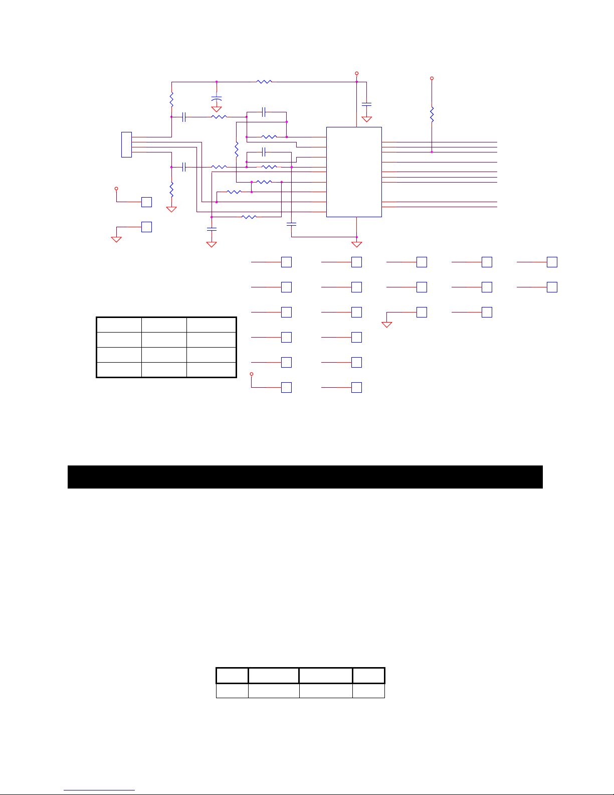
Figure 1: EW681xxxES Board Schematics Telephone Handset Default Diagram
4 Connecting Microphone and Speaker to the W681xxxES
J23 can be used to connect an RJ9 plug from a “standard” telephone handset or headset to the
appropriate pins on the board (Table 4.0). The default resistor and capacitor values on the board are used
for the maximum amplification with no saturation of a 32ohm speaker using a standard microphone.
Unfortunately the only thing “standard” about the RJ9 handset jack is that the microphone and speaker are
always on the same pins. BUT, the microphone polarity can be positive, or negative, depending upon how
the manufacturer designed their telephone set. This means that one has about a 50% chance of wiring it
up wrong the first time UNLESS you know ahead of time which polarity handset you have. Many years
ago, with carbon microphones acting as variable resistors this was not an issue. But with today’s modern
handsets using polarized electret microphones polarity is very important. The circuit in Figure 1 assumes
that the positive side of the microphone is connected to pin 1 of the RJ9 plug and the negative side to pin 4.
Reversing the wires from the RJ9 to the holes in J23 will solve the polarity problem if there is no audio.
Table 4.0 : J23 Pin assignments
3

Note: It is recommended to use short wires to hook up this board to the prototype system for minimal
added noise.
4.1 Adjusting the Amplifier levels for optimal performance
In the handset, application the gain from the handset microphone is set to 27 for the input amplifier. This is
because the acoustical chamber in the telephone type handset lets the electret microphone provide an
output of ~28 mVRMS. The chamber typically has a gain of three over a bare microphone (or one placed
with only a small opening to the outside world.) Because of the high sensitivity of the earphone (150 Ώ
impedance) in a typical handset, the output gain from the Power Amp is set to ~0.16 for a satisfactory
listening level.
SCHEMATIC
COMPONENT #
TELEPHONE
HANDSET
(Values Populated
on the board)
VoIP PHONE SET
(No acoustic
Chamber)
600ΏLINE IN/OUT
(Tip/Ring)
R3,4 1K 1K 10K
R5,6 27K 91K 10K
C7,8 1200 pF 330 pF N/U
R9 SELECT SELECT N/U
R7 20K 20K 27k
R8 3K 3K 27k
Table 4.1: Suggested Components Values By Application
In the VoIP telephone, or small wireless phones, the plastic case is typically too small to provide a
reasonable acoustic chamber. Thus the output from the microphone is less than in the previous example.
This results in having to set the input gain of the CODEC to ~75 to 90. This results in a comparable signal
level to the receive telephone handset but, because of the increased gain, the Signal-to-Noise Ratio (SNR)
has decreased and the signal sounds noisier. On the receive side, the gain is set as in the previous
example. When the Power Amp gain is as low as 0.16 a 32 ohm load can be driven.
If the CODEC is used in a telephone Line Card or a VoIP gateway to the external telephone network then it
will usually be set for 0TLP in and out. This means that the input gain and output gain will be 1:1 and the
values of resistors will be different again. Note that the output of RO- is at 0TLP and going differential will
double this level out of the Power Amp. However, R13 and R14 are 300 ohm resistors to match to the 600
ohm line and the voltage presented to the line will be 0TLP.
Resistor R9 sets the side-tone level (the signal fed back to the ear piece from the microphone so the
telephone sounds “live”) to the level desired by the designer. In most 600 ohm audio line applications, this
feature is not needed. R11 is a just a 0 ohm jumper to allow the board to be used with more than one
model of CODEC. See the chart. R12 is a pull-up resistor for the PCM Transmit line if there is not one
elsewhere in the application.
4

PAI
PAO+
PAO-
R4 1K
C8
330 pF
LS1
32 Ohm SPEAKER
R6 91K
R5 91K
R7 20K
VDD
+
-
VAG
R2
1.5K
C7 330 pF
R1
1.5K
RO-
R9
SELECT
M1
C4 4.7uF
SIDETONE LEVEL CONTROL
C3 0.1uF
AO
R10
1K
AI+
R8 3K
AI-
TO FILTERS AND ENCODER
R3 1K
FROM FILTER AND DECODER
C2 0.1uF
Figure 2: VoIP Phone Set Diagram
C3 0.1uF
to 600 Ohm Line/Load
R14 300 OHM
Note: R13 and R14
are not on board
R6 10K
R8 27K
R13 300 OHM
AI-
VAG
R7 27K
RO-
C2 0.1uF
TO FILTERS AND ENCODER
LINE IN
R3 10K
R5 10K
FROM FILTER AND DECODER
+
-
AI+
LINE OUT
R4 10K
PAI
PAO+
PAO-
AO
Figure 3: 600 Ohm Line IN/OUT Diagram
5

5 Ordering information
Table 5.0 describes the various CODEC Evaluation Systems.
Evaluation Board part Number
Winbond Codec Part number
W6810ES W6810IR
W681512ES W681512R
W681310 ES W681310R
Table 5.0: W681xxxES Part Number
Headquarters Winbond Electronics Corporation America Winbond Electronics (Shanghai) Ltd.
No. 4, Creation Rd. III 2727 North First Street, San Jose, 27F, 299 Yan An W. Rd. Shanghai,
Science-Based Industrial Park, CA 95134, U.S.A. 200336 China
Hsinchu, Taiwan TEL: 1-408-9436666 TEL: 86-21-62365999
TEL: 886-3-5770066 FAX: 1-408-5441798 FAX: 86-21-62356998
FAX: 886-3-5665577 http://www.winbond-usa.com/
http://www.winbond.com.tw/
Taipei Office Winbond Electronics Corporation Japan Winbond Electronics (H.K.) Ltd.
9F, No. 480, Pueiguang Rd. 7F Daini-ueno BLDG, 3-7-18 Unit 9-15, 22F, Millennium City,
Neihu District, Shinyokohama Kohoku-ku, No. 378 Kwun Tong Rd.,
Taipei, 114, Taiwan Yokohama, 222-0033 Kowloon, Hong Kong
TEL: 886-2-81777168 TEL: 81-45-4781881 TEL: 852-27513100
FAX: 886-2-87153579 FAX: 81-45-4781800 FAX: 852-27552064
Please note that all data and specifications are subject to change without notice.
All the trademarks of products and companies mentioned in this datasheet belong to their respective owners.
The information contained in this datasheet may be subject to change
without notice. It is the responsibility of the customer to check the
Winbond USA website (www.winbond-usa.com) periodically for the latest
version of this document, and an
y
Errata Sheets that ma
y
be
g
enerated
6
This manual suits for next models
2
Table of contents
Other Winbond Motherboard manuals