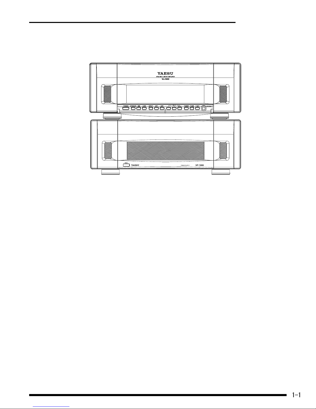
VL-1000 Technical Supplement
Chip Component Information
Replacing Chip Components
Chip components are installed at the factory
by a series of robots. The first one places a small
spot of adhesive resin at the location where each
part is to be installed, and later robots handle
and place parts using vacuum suction.
For single sided boards, solder paste is applied
and the board is then baked to harden the resin
and flow the solder. For double sided boards, no
solder paste is applied, but the board is baked
(or exposed to ultra-violet light) to cure the resin
before dip soldering.
In our laboratories and service shops, small
quantities of chip components are mounted man-
ually by applying a spot of resin, placing the com-
ponents with tweezers, and then soldering by
very small dual streams of hot air (without phys-
ical contact during soldering). We remove parts
by first removing solder using a vacuum suction
iron, which applies a light steady vacuum at the
iron tip, and then breaking the adhesive with
tweezers.
Special vacuum/desoldering equipment is
recommended if you expect to do a lot of chip
replacements. Otherwise, it is usually possible
to remove and replace chip components with
only a tapered, temperature-controlled solder-
ing iron, a set of tweezers and braided copper
solder wick. Soldering iron temperature should
be below 280°C (536°F).
Precautions for Chip Replacement
Do not disconnect a chip forcefully, or the
foil pattern may peel off the board.
Never re-use a chip component. Dispose of
all removed chip components immediate-
ly to avoid mixing with new parts.
Limit soldering time to 3 seconds or less to
avoid damaging the component and board.
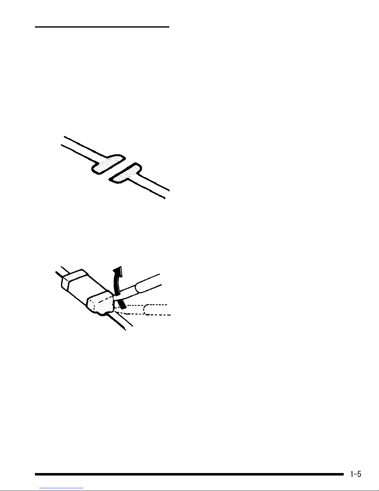
Removing Chip Components
Remove the solder at each joint, one joint at a
time, using solder wick whetted with nona-
cidic fluxes as shown below. Avoid applying
pressure, and do not attempt to remove tin-
ning from the chip’s electrode.
Grasp the chip on both sides with tweezers,
and gently twist the tweezers back and forth
(to break the adhesive bond) while alternate-
ly heating each electrode. Be careful to avoid
peeling the foil traces from the board.
Dispose of the chip when removed.
After removing the chip, use the copper braid
and soldering iron to wick away any excess
solder and smooth the land for installation of
the replacement part.