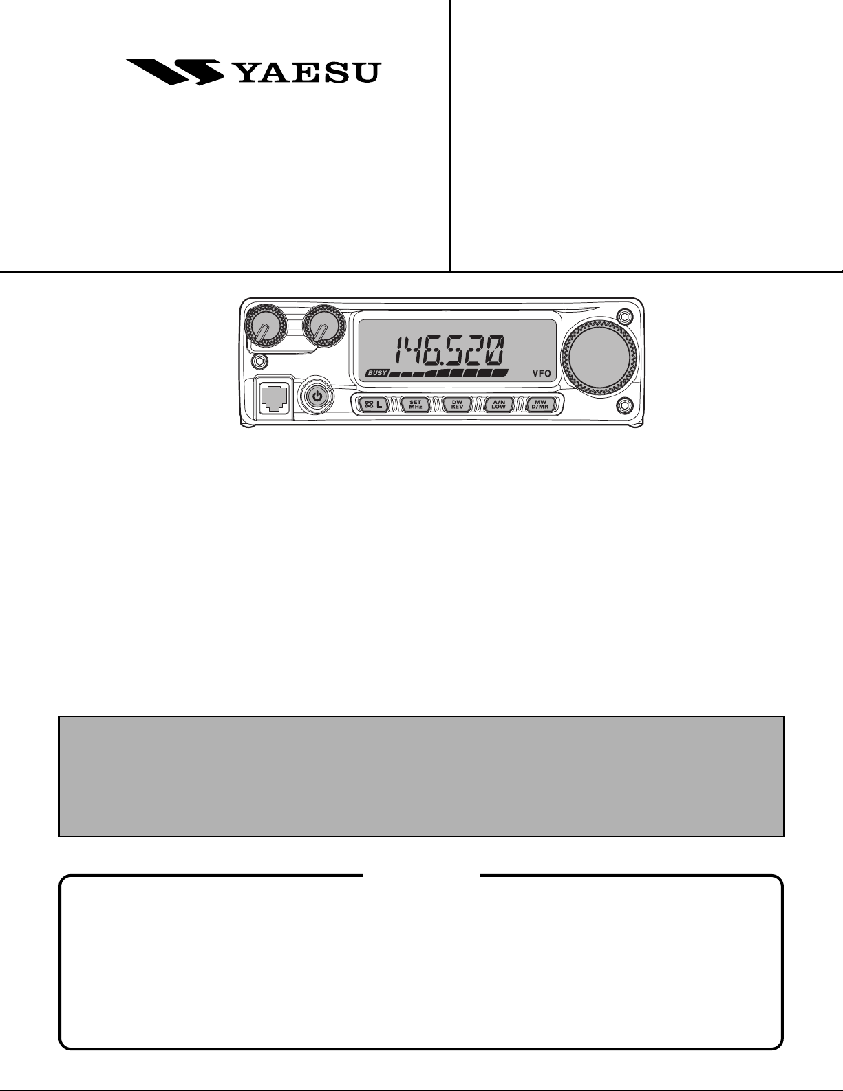
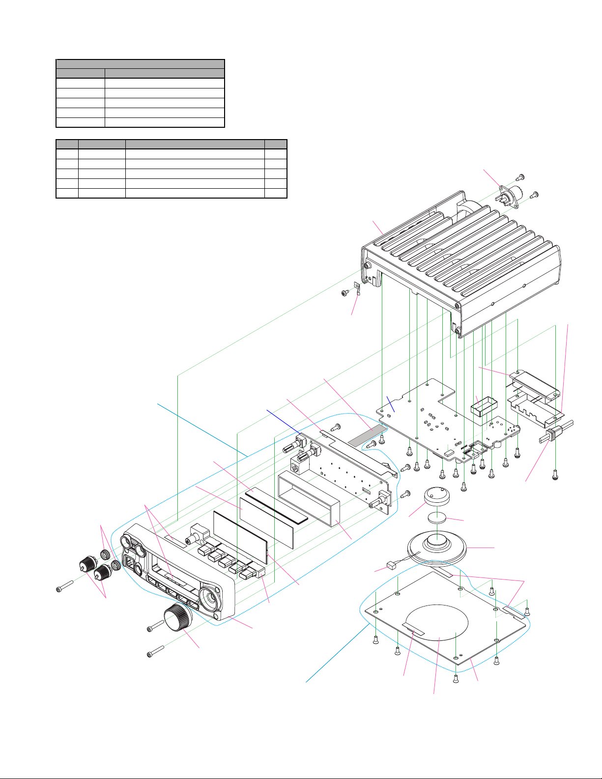
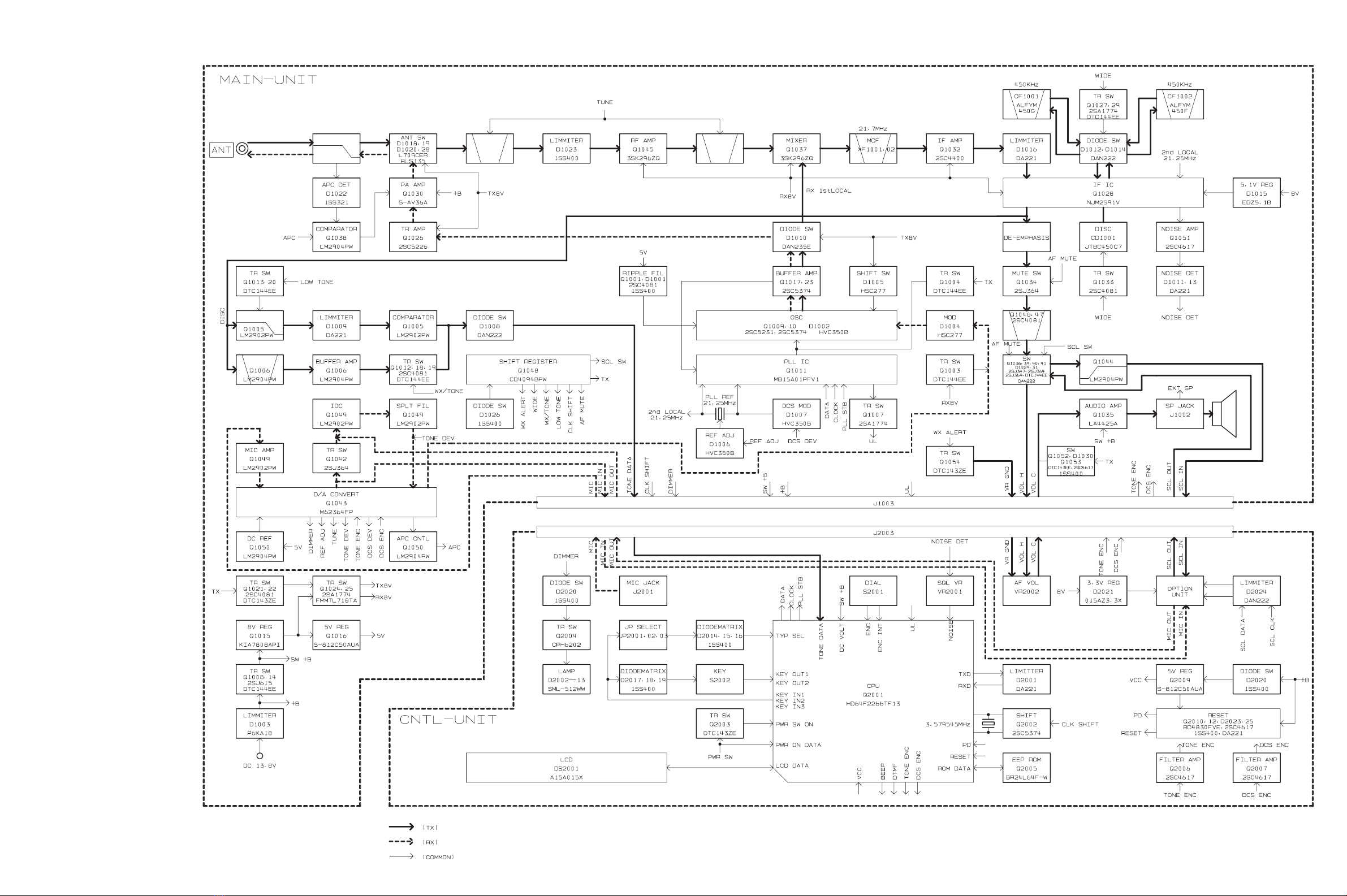
Yaesu FT-2900R Manual

1
Introduction
This manual provides technical information necessary for servicing the FT-2900R FM Transceiver.
Servicing this equipment requires expertise in handling surface-mount chip components. Attempts by non-
qualified persons to service this equipment may result in permanent damage not covered by the warranty,
and may be illegal in some countries.
Two PCB layout diagrams are provided for each double-sided circuit board in the Transceiver. Each side of is
referred to by the type of the majority of components installed on that side (“leaded” or “chip-only”). In most
cases one side has only chip components, and the other has either a mixture of both chip and leaded compo-
nents (trimmers, coils, electrolytic capacitors, ICs, etc.), or leaded components only.
While we believe the technical information in this manual to be correct, VERTEX STANDARD assumes no
liability for damage that may occur as a result of typographical or other errors that may be present. Your
cooperation in pointing out any inconsistencies in the technical information would be appreciated.
©2009 VERTEX STANDARD CO., LTD. EH039N90A
Technical Supplement
Specifications ...................................................... 2
Exploded View & Miscellaneous Parts ............ 3
Block Diagram .................................................... 5
Connection Diagram .......................................... 6
Circuit Description............................................. 7
Alignment ............................................................ 9
Contents
Board Unit (
Schematics, Layouts & Parts
)
MAIN Unit Circuit Diagram ................................. 13
MAIN Unit Parts Layout ....................................... 15
MAIN Unit Parts List ............................................ 17
CNTL Unit Circuit Diagram ................................. 27
CNTL Parts Layout ............................................... 28
CNTL Parts List .................................................... 29
FM TRANSCEIVER
FT-2900R
VERTEX STANDARD CO., LTD.
4-8-8 Nakameguro, Meguro-Ku, Tokyo 153-8644, Japan
VERTEX STANDARD
US Headquarters
10900 Walker Street, Cypress, CA 90630, U.S.A.
YAESU UK LTD.
Unit 12, Sun Valley Business Park, Winnall Close
Winchester, Hampshire, SO23 0LB, U.K.
VERTEX STANDARD HK LTD.
Unit 5, 20/F., Seaview Centre, 139-141 Hoi Bun Road,
Kwun Tong, Kowloon, Hong Kong
VERTEX STANDARD (AUSTRALIA)PTY., LTD.
Normanby Business Park, Unit 14/45 Normanby Road
Notting Hill 3168, Victoria, Australia
Important Note
The transceiver was assembled using Pb (lead) free solder, based on the RoHS specification.
Only lead-free solder (Alloy Composition: Sn-3.0Ag-0.5Cu) should be used for repairs performed on this appara-
tus. The solder stated above utilizes the alloy composition required for compliance with the lead-free specification,
and any solder with the above alloy composition may be used.

2
Specifications
General
Frequency Range: Tx 144 - 146 MHz or 144 - 148 MHz
Rx 144 - 146 MHz or 136 - 174 MHz
Channel Step: 5/10/12.5/15/20/25/50/100 kHz
Standard Repeater Shift: ±600 kHz
Frequency Stability: Better than ±10 ppm [–4 °F to +140 °F (–20 °C to +60 °C)]
Modes of Emission: F2D/F3E
Antenna Impedance: 50 Ohms, unbalanced
Supply voltage: 13.8 V DC ±15%, negative ground
Current Consumption (typical): Rx: less than 0.7 A, less than 0.3 A (squelched)
Tx: 15 A (75 W) /9 A (30 W) /5 A (10 W) /4 A (5 W)
Operating Temperature Range: –4° F to +140° F (–20° C to +60° C)
Case Size (WxHxD): 6.3” x 2” x 7.3” (160 x 50 x 185 mm) (w/o knobs)
Weight (Approx.): 4.2 lb (1.9 kg)
Transmitter
Output Power: 75 W/30 W/10 W/5 W
Modulation Type: Variable Reactance
Maximum Deviation: ±5 kHz (Wide)/±2.5 kHz (Narrow)
Spurious Radiation: Better than –60 dB
Microphone Impedance: 2 k-Ohms
Receiver
Circuit Type: Double Conversion Superheterodyne
Ifs: 21.7 MHz & 450 kHz
Sensitivity (for 12dB SINAD): Better than 0.2 µV
Selectivity (–6/–60dB): 12 kHz/28 kHz (Wide)
9 kHz/22 kHz (Narrow)
IF Rejection: Better than 70 dB
Image Rejection: Better than 70 dB
Maximum AF Output: 3 W into 4 Ohms @10 % THD
Specifications subject to change without notice or obligation. Specifications guaranteed only within Amateur band.
Frequency ranges and functions will vary according to transceiver version; check with your dealer.

3
Exploded View & Miscellaneous Parts
g
d
g
d
d
d
e
e
M4090178
SPEAKER
Non-designated parts are available only as part of a
designated assembly.
S8002063
CAP-SP
RA1104900
FRONT PANEL
RA1105000
RUBBER KNOB
G6090192
LCD
RA1131200
INTER CONNECTOR
S8002060
FILTER LCD
CNTL UNIT
MAIN UNIT
RA1120000
GROUND PLATE
RA1113700
CHASSIS
RA1120800
ENCODER KNOB
RA1120700 (x2 pcs)
KNOB (VOL/SQL)
S8002056
REFLECTOR
P1091172
CONNECTOR
G1094704
S-AV36A
T9207482
WIRE ASSY
REF.
c
d
e
f
g
QTY.
4
5
11
6
3
DESCRIPTION
SEMS SCREW ASM3X10NI
BIND HEAD TAPTITE-B M3X10
TAPTITE SCREW M3X8NI
FLAT HEAD SCREW M3X8B
HEXA SOCKET BOLT M3X20B
VXSTD P/N
U03310002
U24310001
U24308002
U30308007
U51320007
T9207248
WIRE ASSY
T9206438A
WIRE ASSY
g
RA0210600
RUBBER PACKING
d
c
e
c
e
c
c
e
e
e
e
e
e
e
f
f
f
f
f
f
RA1142100
GROUND PLATE
RA0124501
SHIELD CASE
S8002088
FELT
DESCRIPTION
MICROPHONE (MH-48A6J)
DC CABLE
SPARE FUSE (25 A)
FOOT
BRACKET (MMB-83)
VXSTD P/N
AAA43X001
T9025825
Q0000074
S8002050
RA1119800
ACCESSORIES
RA1150500
PORON SHEET (D20x2)
RA0515300
SHIELD CASE
RA1113800
BOTTOM COVER (H039)
S8002087
NET-SP
RA1148000
SHEET 45x5
RA1148000
SHEET 45x5
CS2042401 TYP:A2
CS2042402 TYP:A1
CS2042403 TYP:A3
CS2042404 TYP:B1
CS2042405 TYP:B2
CS2042406 TYP:B3
FRONT PANEL ASSY
CP9508001
BOTTOM COVER ASSY

4
Note

5
Block Diagram

6
Connection Diagram

7
Circuit Description
Receive Signal Path
Incoming RF signal is from the antenna jack is deliv-
ered to the Main Unit and passed through the low-
pass filter network consisting capacitors C1213,
C1236, C1238, C1239, & C1241 and coils L1017, L1018,
& L1019, antenna switching diode D1020 and D1028
(both RLS135), and varactor-tuned band-pass filter
consisting of capacitors C1248, C1249, C1250, C1251,
C1252, & C1268, coils L1020, L1021, & L1024, and
diodes D1024 and D1025 (both HVC350B), before
delivery to the RF amplifier Q1045 (3SK296ZQ). The
amplified RF signal is passed through the another
varactor-tuned band-pass filter consisting of capac-
itors C1198, 1199, 1200, & 1218, coils L1012 and L1015,
and diodes D1017 and D1021 (both HVC350B), then
applied to the 1st mixer Q1037 (3SK296ZQ) along
with the first local signal from the PLL circuit.
The first local signal is generated between 114.3 MHz
and 152.3 MHz by the VCO, which consists of Q1009
(2SC5231) and varactor diode D1002 (HVC350B) ac-
cording to the receiving frequency.
IF and Audio Circuits
The 21.7 MHz first IF signal is applied to the mono-
lithic crystal filters XF1001 and XF1002 which strip
away unwanted mixer products, and the IF signal is
applied to the first IF amplifier Q1032 (2SC4400).
The amplified first IF signal is then delivered to the
FM IF subsystem IC Q1028 (NJM2591V), which con-
tains the second mixer, limiter amplifier, noise am-
plifier, and FM detector.
The second local signal is generated by 21.25 MHz
crystal X1001, produces the 450 kHz second IF sig-
nal when mixed with first IF signal within Q1028
(NJM2591V).
The 450 kHz second IF signal is applied to the ce-
ramic filter CF1001 (for Narrow FM) or CF1002 (for
Wide FM) which strip away unwanted mixer prod-
ucts to the ceramic discriminator CD1001 which re-
moves any amplitude variations in the 450 kHz IF
signal before detection of speech.
The detected audio from the Q1028 (NJM2591V)
passes through the de-emphasis circuit consisting of
resistors R1082 & R1113, and capacitors C1120 &
C1122, to the audio mute gate Q1034 (2SJ364).
The audio signal passes through a band-pass filter
consisting of Q1046 and Q1047 (both 2SC4081), and
the audio mute gate Q1039 (2SJ347), to the audio
VR which adjusts the audio sensitivity to compen-
sate for audio level variations. The adjusted audio
signal is delivered to the audio amplifier Q1035
(LA4425A) which provides up to 3 Watts, to the ex-
ternal speaker jack or a 4-Ohm loudspeaker.
Squelch Control
When no carrier received, the noise signal from
Q1028 (NJM2591V) is amplified by Q1051
(2SC4617), and is detected by D1011 and D1013
(both DA221). The resulting DC voltage passes
through the SQL knob to main CPU Q2001
(HD64F2266TF13). While no carrier is received,
main CPU Q2001 (HD64F2266TF13) control Q1048
(CD4094BPWR), thus, audio mute gate Q1034
(2SJ364) and Q1039 (2SJ347) turns “OFF” to dis-
able the audio output from the speaker.
Transmit Signal Path
The speech signal from the microphone is amplified
by Q1049 (LM2902PWR). The amplified speech sig-
nal is subjected to the low-pass filter network Q1049
(LM2902PWR) to deviation controlled by Q1043
(M62364FP).
The adjusted speech signal from Q1043 (M62364FP)
is delivered to VCO Q1009 (2SC5231) which fre-
quency modulates the transmitting VCO made up
of D1004 (HSC277).
The modulated transmit signal passes through buff-
er amplifier Q1010 and Q1023 (both 2SC5374).
The transmit signal applied to the drive amplifier
Q1026 (2SC5226), then finally amplified by power
amplifier module Q1030 (S-AV36A) up to 75 Watts.
The APC circuit controls the Q1030 (S-AV36A) pow-
er amplifier’s gain.
The 75 Watts RF signal passes through low-pass fil-
ter network consisting of Capacitors C1210 and
C1211 and coil L1013, antenna switch D1018 and
D1019 (both L709CER), and another low-pass filter
network consisting capacitors C1213, C1236, C1238,
C1239, & C1241 and coils L1017, L1018, & L1019, and
then deliver to the ANT jack.

8
Circuit Description
TX APC Circuit
A portion of the power amplifier module output is
rectified by D1022 (1SS321), then delivered to APC
Q1038 (LM2904PWR), as a DC voltage which is pro-
portional to the output level of the power amplifier
module.
The APC Q1038 (LM2904PWR) is compared the rec-
tified DC voltage from the power amplifier module
and the reference voltage from the main CPU Q2001
(HD64F2266TF13), to produce a control voltage,
which regulates supply voltage to the power ampli-
fier module Q1030 (S-AV36A), so as to maintain sta-
ble output power under varying antenna loading
condition.
PLL
A portion of the output from the VCO Q1009
(2SC5231) passes through the buffer amplifier
Q1010 and Q1017 (both 2SC5374), then delivered
to the programmable divider section of the PLL IC
Q1011 (MB15A01PFV1), which divided according
to the frequency dividing data that is associated with
the setting frequency input from the main CPU
Q2001 (HD64F2266TF13). It is then sent to the phase
comparator section of the PLL IC Q1011
(MB15A01PFV1).
The 21.25 MHz frequency of the reference oscillator
circuit made up of X1001 is divided by the reference
frequency divider section of Q1011 (MB15A01PFV1)
into 4250 or 3400 parts to become 5 kHz or 6.25 kHz
comparative reference frequencies, which are uti-
lized by the phase comparator section of Q1011
(MB15A01PFV1).
The phase comparator section of Q1011
(MB15A01PFV1) compares the phase between the
frequency-divided oscillation frequency of the VCO
circuit and comparative frequency and its output is
a pulse corresponding to the phase difference. This
pulse is integrated by the charge pump and loop fil-
ter into a control voltage (VCV) to control the oscil-
lation frequency of the VCO Q1009 (2SC5231).

9
Alignment
Introduction
The FT-2900R is carefully aligned at the factory for
the specified performance across the amateur band.
Realignment should therefore not be necessary ex-
cept in the event of a component failure. Only an
authorized Vertex Standard representative should
perform all component replacement and service, or
the warranty policy may be void.
The following procedures cover the adjustments that
are not normally required once the transceiver has
left the factory. However, if damage occurs and some
parts subsequently are replaced, realignment may
be required. If a sudden problem occurs during nor-
mal operation, it is likely due to component failure;
realignment should not be done until after the faulty
component has been replaced.
We recommend that servicing be performed only by
authorized Vertex Standard service technicians who
are experienced with the circuitry and fully equipped
for repair and alignment. If a fault is suspected, con-
tact the dealer from whom the transceiver was pur-
chased for instructions regarding repair. Authorized
Vertex Standard service technicians realign all cir-
cuits and make complete performance checks to en-
sure compliance with factory specifications after re-
placing any faulty components.
Those who do undertake any of the following align-
ments are cautioned to proceed at their own risk.
Problems caused by unauthorized attempts at re-
alignment are not covered by the warranty policy.
Also, Vertex Standard reserves the right to change
circuits and alignment procedures in the interest of
improved performance, without notifying owners.
Under no circumstances should any alignment be
attempted unless the normal function and operation
of the transceiver are clearly understood, the cause
of the malfunction has been clearly pinpointed and
any faulty components replaced, and realignment
determined to be absolutely necessary.
Required Test Equipment
The following test equipment (and familiarity with
its use) is necessary for complete realignment. Cor-
rection of problems caused by misalignment result-
ing from use of improper test equipment is not cov-
ered under the warranty policy. While most steps
do not require all of the equipment listed, the inter-
actions of some adjustments may require that more
complex adjustments be performed afterwards.
Do not attempt to perform only a single step unless
it is clearly isolated electrically from all other steps.
Have all test equipment ready before beginning and,
follow all of the steps in a section in the order pre-
sented.
RF Signal Generator with calibrated output level
at 200 MHz
Deviation Meter (linear detector)
In-line Wattmeter with 5% accuracy at 200 MHz
50-Ohm 100-W RF Dummy Load
8-Ohm AF Dummy Load
Regulated DC Power Supply adjustable from 9 to
16.5 VDC, 20A
Frequency Counter: 0.2-ppm accuracy at 200 MHz
AF Signal Generator
AC Voltmeter
DC Voltmeter: high impedance
VHF Sampling Coupler
SINAD Meter

10
Alignment Preparation & Precautions
A 50-Ohm RF load and in-line wattmeter must be
connected to the antenna jack in all procedures that
call for transmission; alignment is not possible with
an antenna. After completing one step, read the next
step to see if the same test equipment is required. If
not, remove the test equipment (except dummy load
and wattmeter, if connected) before proceeding.
Correct alignment requires that the ambient tem-
perature be the same as that of the transceiver and
test equipment, and that this temperature be held
constant between 68 °F ~ 86 °F (20 °C ~ 30 °C). When
the transceiver is brought into the shop from hot or
cold air, it should be allowed some time to come to
room temperature before alignment. Whenever pos-
sible, alignments should be made with oscillator
shields and circuit boards firmly affixed in place.
Also, the test equipment must be thoroughly
warmed up before beginning.
Note: Signal levels in dB referred to in the alignment
procedure are based on 0dBµ = 0.5µV.
Test Setup
Set up the test equipment as shown below for trans-
ceiver alignment.
Entering the Alignment Mode
Alignment of the FT-2900R is performed using a front
panel software-based procedure. To perform align-
ment of the transceiver, it must first be placed in the
“Alignment Mode,” in which the adjustments will
be made and then stored into memory.
To enter the Alignment mode:
1. Press and hold in the [MHz(SET)] key while turning
the radio on.
2. Press and hold in the [PWR()] switch for 1/2 sec-
ond to turn the radio off.
3. To enter the Alignment mode, press and hold in the
[REV(DW)] and [D/MR(MW)] keys while turning the
radio on. Once the radio is on, release these two key.
The transceiver is now in the “Alignment Mode.”
PLL Reference Frequency
Rotate the DIAL knob to set the alignment param-
eter to “B0201 rFB0201 rF
B0201 rFB0201 rF
B0201 rF.”
Press the [D/MR(MW)] key to enable adjustment
of the “PLL Reference Frequency.”
Press the PTT switch to activate the transmitter,
adjust the DIAL knob so that the counter fre-
quency reading is 146.000 MHz (±80 Hz).
Press the [D/MR(MW)] key.
RF Front-end Tuning
Inject a 145.100 MHz signal at a level of –10 dBµ
(with 1 kHz modulation @±3.5 kHz deviation)
from the RF signal generator.
Rotate the DIAL knob to set the alignment param-
eter to “B0111 tnB0111 tn
B0111 tnB0111 tn
B0111 tn.”
Press the [D/MR(MW)] key to enable adjustment
of the “RF Front-end Tuning.”
Adjust the DIAL knob so that the maximum
SINAD.
Press the [D/MR(MW)] key.
Squelch Threshold Level
Inject a 145.100 MHz signal at a level of –14 dBµ
(with 1 kHz modulation @±3.5 kHz deviation)
from the RF signal generator.
Rotate the SQL knob to the 10-o’clocl position.
Rotate the DIAL knob to set the alignment param-
eter to “B0111 tLB0111 tL
B0111 tLB0111 tL
B0111 tL.”
Press the [D/MR(MW)] key to enable adjustment
of the “Squelch Threshold Level.”
Press the [D/MR(MW)] key three times.
Press the [D/MR(MW)] key.
Alignment
TEST EQUIPMENT SETUP
MIC SW2
MIC SW1
GND +8V
MIC INPUT
PTT/CLONE
FT-2900R
Inline
Wattmeter
SINAD MeterDeviation Meter
Frequency
Counter
RF
Signal Generator
AF
Signal Generator
RF
Signal Generator
50-Ohm
Dummy Load
MIC
ANT
EXT SP
RF Sampling
Coupler
DC INPUT

11
S-meter Level (S-1)
Inject a 145.100 MHz signal at a level of –5 dBµ
(with 1 kHz modulation @±3.5 kHz deviation)
from the RF signal generator.
Rotate the DIAL knob to set the alignment param-
eter to “B0111 S1B0111 S1
B0111 S1B0111 S1
B0111 S1.”
Press the [D/MR(MW)] key to enable adjustment
of the “S-meter Level (S-1).”
Press the [D/MR(MW)] key three times.
Press the [D/MR(MW)] key.
S-meter Level (S-9)
Inject a 145.100 MHz signal at a level of +23 dBµ
(with 1 kHz modulation @±3.5 kHz deviation)
from the RF signal generator.
Rotate the DIAL knob to set the alignment param-
eter to “B0111 S9B0111 S9
B0111 S9B0111 S9
B0111 S9.”
Press the [D/MR(MW)] key to enable adjustment
of the “S-meter Level (S-9).”
Press the [D/MR(MW)] key three times.
Press the [D/MR(MW)] key.
TX Power (High)
Rotate the DIAL knob to set the alignment param-
eter to “B0101 HPB0101 HP
B0101 HPB0101 HP
B0101 HP.”
Press the [D/MR(MW)] key to enable adjustment
of the “TX Power (High).”
Press the PTT switch to activate the transmitter,
adjust the DIAL knob so that the RF Power Meter
reading is 75 W (±3.0W).
Press the [D/MR(MW)] key.
TX Power (Low 3)
Rotate the DIAL knob to set the alignment param-
eter to “B0101 L3B0101 L3
B0101 L3B0101 L3
B0101 L3.”
Press the [D/MR(MW)] key to enable adjustment
of the “TX Power (Low 3).”
Press the PTT switch to activate the transmitter,
adjust the DIAL knob so that the RF Power Meter
reading is 30 W (±1.5 W).
Press the [D/MR(MW)] key.
TX Power (Low 2)
Rotate the DIAL knob to set the alignment param-
eter to “B0101 L2B0101 L2
B0101 L2B0101 L2
B0101 L2.”
Press the [D/MR(MW)] key to enable adjustment
of the “TX Power (Low 2).”
Press the PTT switch to activate the transmitter,
adjust the DIAL knob so that the RF Power Meter
reading is 10 W (±1.0 W).
Press the [D/MR(MW)] key.
TX Power (Low 1)
Rotate the DIAL knob to set the alignment param-
eter to “B0101 L1B0101 L1
B0101 L1B0101 L1
B0101 L1.”
Press the [D/MR(MW)] key to enable adjustment
of the “TX Power (Low 1).”
Press the PTT switch to activate the transmitter,
adjust the DIAL knob so that the RF Power Meter
reading is 5 W (±0.5 W).
Press the [D/MR(MW)] key.
TX Deviation
Inject a 1 kHz, 50 mV signal from the Audio Gen-
erator.
Rotate the DIAL knob to set the alignment param-
eter to “B0101 dUB0101 dU
B0101 dUB0101 dU
B0101 dU.”
Press the [D/MR(MW)] key to enable adjustment
of the “TX Deviation.”
Press the PTT switch to activate the transmitter,
adjust the DIAL knob so that the Deviation Meter
reading is 4.2 kHz (±0.1 kHz).
Press the [D/MR(MW)] key.
CTCSS TX Deviation
Rotate the DIAL knob to set the alignment param-
eter to “B0101 100B0101 100
B0101 100B0101 100
B0101 100.”
Press the [D/MR(MW)] key to enable adjustment
of the “CTCSS TX Deviation.”
Press the PTT switch to activate the transmitter,
adjust the DIAL knob so that the Deviation Meter
reading is 0.6 kHz (±0.05 kHz).
Press the [D/MR(MW)] key.
Alignment

12
DCS TX Deviation
Rotate the DIAL knob to set the alignment param-
eter to “B0101 dCB0101 dC
B0101 dCB0101 dC
B0101 dC.”
Press the [D/MR(MW)] key to enable adjustment
of the “DCS TX Deviation.”
Press the PTT switch to activate the transmitter,
adjust the DIAL knob so that the Deviation Meter
reading is 0.8 kHz (±0.05 kHz).
Press the [D/MR(MW)] key.
Alignment
Closing the Alignment mode
1. Press the [DW(REV)] key to save the new setting and
exit to normal operation.
2. Press and hold in the [PWR()] switch for 1/2 sec-
ond to turn the radio off.
3. Press and hold in the [MHz(SET)] key while turning
the radio on.

13
MAIN Unit
Circuit Diagram
4.3 V (4.3 V)
4.9 V (4.9 V)
4.0 V (4.0 V)
2.0 V (2.0 V)
1.3 V (1.3 V)
0.7 V (0.7 V)
3.4 V
(3.4 V)
3.3 V
(3.3 V)
0.6 V (0.6 V)
0.7 V
(0.6 V)
6.2 V (4.5 V)
0.0 V (5.3 V)
7.0 V (0.0 V)
0.0 V (1.6 V)
0.0 V (1.2 V)
0.0 V (7.0 V)
5.1 V (0.0 V)
4.9 V
(0.0 V)
2.3 V
(0.0 V)
0.0 V (0.0 V)
0.0 V (0.0 V)
2.8 V (0.0 V)
5.1 V (0.0 V)
4.5 V
(0.0 V)
5.0 V (0.0 V)
0.6 V (0.0 V)
1.3 V (0.0 V)
0.9 V (0.0 V)
2.3 V (2.3 V)
1.4 V
(0.0 V)
2.3 V
(0.0 V)
0.6 V (0.0 V)
1.8 V (0.0 V)
5.0 V
(5.0 V)
4.8 V
(4.8 V)
1.2 V
(1.5 V)
4.6 V
(4.6 V)
4.8 V
(4.8 V)
0.0 V (0.0 V)
Low 1 : 0.0 V (2.8 V)
Low 2 : 0.0 V (3.0 V)
Low 3 : 0.0 V (3.3 V)
HIGH : 0.0 V (4.0 V)
2.9 V (2.9 V)
0.7 V (0.0 V)
6.5 V (0.0 V)
0.3 V (0.0 V)
1.0 V (0.0 V)
7.6 V
(0.0 V) 1.4 V (0.0 V)
Low 1 : 0.0 V (0.7 V)
Low 2 : 0.0 V (1.0 V)
Low 3 : 0.0 V (1.8 V)
HIGH : 0.0 V (2.9 V)
Low 1 : 0.0 V (0.6 V)
Low 2 : 0.0 V (0.9 V)
Low 3 : 0.0 V (1.7 V)
HIGH : 0.0 V (2.9 V)
0.0 V (1.7 V)
6.7 V
(0.0 V)
4.8 V
(0.0 V) 1.5 V (0.0 V)
1.1 V
(0.0 V)
2.2 V (0.7 V)
1.5 V (0.0 V)
0.9 V (0.0 V)
3.1 V
(0.0 V)
2.5 V (0.3 V)
5.4 V
(0.0 V)
2.6 V
(0.0 V)
2.5 V (0.3 V)
2.5 V (0.8 V)
0.0 V (0.9 V)
0.0 V (0.0 V)
7.4 V
(4.6 V)
0.0 V
(0.0 V)
0.0 V (0.0 V)
0.0 V
(0.0 V)
0.0 V (0.0 V)
0.0 V (0.0 V)
0.0 V (4.9 V)
0.35 Vp-p
(0.0 V)
0.0 V (0.8 Vp-p)
0.6 V (0.0 V)
0.0 V (0.0 V)
7.0 Vp-p (0.0 V) WX Alert 1050 Hz
DEV 3 kHz
2.2 V (0.0 V)
5.0 Vp-p (0.0 V) TONE 100 Hz
DEV 0.7 kHz
6.0 Vp-p (0.0 V) TONE 100 Hz
DEV 0.7 kHz
7.0 Vp-p (0.0 V) TONE 100 Hz
DEV 0.7 kHz
7.9 V (0.0 V)
7.2 V (8.0 V)
8.0 V (8.0 V)
0.0 V (7.9 V)
7.8 V (7.2 V)
0.1 V (8.0 V)
7.8 V (7.2 V)
7.8 V (0.0 V)
8.0 V (8.0 V)
8.0 V (8.0 V)
5.0 V (5.0 V)
13.8 V (13.5 V)
0.0 V
(0.0 V)
4.1 V
(4.1 V)
0.0 V (4.0 V)
0.0 V (4.5 V)
0.2 Vp-p (0.0 V)
VOL Max
0.0 V (0.15 Vp-p)
0.0 V (2.5 Vp-p)
DCS On MOD Off
0.0 V
(3.9 V) 0.0 V (3.4 V)
11.0 Vp-p (0.0 V)
VOL Max
0.2 Vp-p (0.0 V)
VOL Max
13.5 V (13.5 V)
0.0 V (0.0 V)
0.0 V (0.0 V)
3.0 Vp-p (3.0 Vp-p)
7.8 V (0.0 V)
0.0 V (4.0 Vp-p)
5.0 V (5.0 V)
0.25 Vp-p
(0.0 V)
0.0 V (0.45 Vp-p)
0.0 V (1.4 Vp-p)
TONE 100 Hz ON
MOD Off
0.0 V (1.5 Vp-p)
DCS ON
MOD Off
0.7 V (0.7 V)
0.0 V (0.2 Vp-p)
TONE 100 Hz ON
MOD Off
2.4 V (2.4 V)
DIMMER 5
0.0 V
(1.0 Vp-p)
0.0 V
(0.51 Vp-p)
3.2 V (0.0 V)
Low 1 : 0.7 V (1.8 V)
Low 2 : 0.7 V (2.1 V)
Low 3 : 0.7 V (2.9 V)
HIGH : 0.7 V (4.0 V)
1.9 V (1.9 V)
5.0 V (5.0 V) 0.0 V (1.4 Vp-p)
0.0 V (3.0 Vp-p)
0.0 V (2.0 Vp-p)
4.9 V (0.0 V)
4.7 V (4.7 V)
0.0 V (5.0 V)
0.0 V (0.0 V)
0.0 V
(0.0 V)
4.6 V (4.6 V)
4.9 V
(4.9 V)
5.0 V (5.0 V)
RX (TX)

14
MAIN Unit
Note

15
MAIN Unit
Parts Layout (Side A)
BADCEFG
1
2
3
4
5
2SA1774 (FR)
(Q1007)
2SC4081 (B)
(Q1033)
2SC4400 (RT4)
(Q1032)
2SC4617 (BR)
(Q1051, 1053)
2SC5226 (R22)
(Q1026)
2SC5231 (C9)
(Q1009)
2SC5374 (NA)
(Q1010, 1017, 1023)
DAN235E (M)
(D1010)
CD4094BPWR
(Q1048)
MB15A01PFV1
(Q1011)
NJM2591V
(Q1028)
2SJ615
(Q1008)
KIA7808API
(Q1015)
LA4425A
(Q1035)
S-AV36A
(Q1030)
DTC144EE (26)
(Q1003, 1004, 1014)
DA221 (26)
(D1011, 1013, 1016)
2SK296ZQ (ZQ)
(Q1037, 1045)
DTC143ZE (E23)
(Q1054)
DTC143EE (23)
(Q1052)

16
MAIN Unit
Parts Layout (Side B)
badcefg
1
2
3
4
5
2SA1774 (FR)
(Q1024, 2027, 1029)
2SC4081 (B)
(Q1001, 1012, 1021,
1046, 1047)
FMMTL718TA
(Q1025)
2SJ364 (4M)
(Q1034, 1036,
1041, 1042)
LM2904PWR
(Q1006, 1038,
1044, 1050)
LM2902PWR
(Q1005, 1049)
DTC144EE (26)
(Q1013, 1018, 1019,
1020, 1031, 1040)
M62364FP
(Q1043)
S-812C50AUA
(Q1016)
1SS321 (F9)
(D1022)
DAN222 (N)
(D1008, 1012, 1014,
1029, 1031)
DA221 (26)
(D1009)
2SJ347 (KS)
(Q1039)
DTC143ZE (E23)
(Q1022)

17
PCB with Components CS2040501 1-
Printed Circuit Board FR020070C 1-
C 1001 CHIP TA.CAP. 10uF 10V TAJA106M010Y K78100072 1- B f4
C 1002 CHIP TA.CAP. 10uF 10V TAJA106M010Y K78100072 1- B f4
C 1003 CHIP CAP. 0.01uF 50V B GRM188B11H103KA01D K22174823 1- B f3
C 1004 CHIP CAP. 0.0047uF 50V B GRM188B11H472KA01D K22174817 1- B d4
C 1005 CHIP CAP. 100pF 50V CH GRM1882C1H101JA01D K22174235 1- A A1
C 1006 CHIP CAP. 0.001uF 50V B GRM188B11H102KA01D K22174821 1- A A1
C 1007 AL.ELECTRO.CAP. 3300uF 16V UVR1C332MHD K40129106 1- A B2
C 1008 CHIP CAP. 0.5pF 50V CK GRM1884C1HR50CZ01D K22174201 1- A B5
C 1009 CHIP CAP. 15pF 50V CH GRM1882C1H150JA01D K22174215 1- A B5
C 1011 CHIP CAP. 0.001uF 50V B GRM188B11H102KA01D K22174821 1- A C5
C 1012 CHIP CAP. 0.001uF 50V B GRM188B11H102KA01D K22174821 1- A B5
C 1013 CHIP CAP. 0.001uF 50V B GRM188B11H102KA01D K22174821 1- A B5
C 1014 CHIP CAP. 0.001uF 50V B GRM188B11H102KA01D K22174821 1- A C5
C 1015 CHIP TA.CAP. 0.1uF 20V TMCP1D104MTRF K78130067 1- A C5
C 1016 CHIP TA.CAP. 0.22uF 20V TMCP1D224MTRF K78130069 1- A C5
C 1017 CHIP TA.CAP. 4.7uF 6.3V TEESVP0J475M8R K78080053 1- A C5
C 1018 CHIP CAP. 0.001uF 50V B GRM155B11H102KA01D K22178809 1- A C5
C 1019 CHIP CAP. 0.047uF 25V B GRM188B11E473KA01D K22144811 1- A C4
C 1020 CHIP CAP. 0.001uF 50V B GRM155B11H102KA01D K22178809 1- A C5
C 1021 CHIP CAP. 0.0082uF 50V B GRM188B11H822KA01D K22174837 1- B d4
C 1022 CHIP CAP. 0.0082uF 50V B GRM188B11H822KA01D K22174837 1- B d4
C 1024 CHIP TA.CAP. 4.7uF 16V TAJA475M016Y K78120079 1- B e3
C 1025 CHIP CAP. 0.01uF 50V B GRM188B11H103KA01D K22174823 1- B d4
C 1026 CHIP CAP. 0.0027uF 50V B GRM188B11H272KA01D K22174814 1- B d4
C 1027 CHIP TA.CAP. 1uF 25V TEESVA1E105M8R K78140013 1- B d4
C 1029 CHIP CAP. 0.01uF 50V B GRM188B11H103KA01D K22174823 1- B f1
C 1030 CHIP CAP. 0.001uF 50V B GRM188B11H102KA01D K22174821 1- A C2
C 1031 CHIP CAP. 0.001uF 50V B GRM188B11H102KA01D K22174821 1- A B3
C 1032 CHIP CAP. 0.001uF 50V B GRM188B11H102KA01D K22174821 1- A C3
C 1033 CHIP CAP. 0.001uF 50V B GRM188B11H102KA01D K22174821 1- A B4
C 1034 CHIP CAP. 0.001uF 50V B GRM188B11H102KA01D K22174821 1- A B4
C 1035 CHIP CAP. 0.001uF 50V B GRM188B11H102KA01D K22174821 1- A B5
C 1036 CHIP CAP. 18pF 50V CH GRM1882C1H180JA01D K22174217 1- A B4
C 1037 CHIP CAP. 20pF 50V CH GRM1882C1H200JZ01D K22174218 1- A B4
C 1038 CHIP CAP. 0.001uF 50V B GRM188B11H102KA01D K22174821 1- A C4
C 1039 CHIP CAP. 1uF 10V F GRM188F11A105ZA01D K22105001 1- A C4
C 1040 CHIP CAP. 1.5pF 50V CK GRM1884C1H1R5CZ01D K22174258 1- A B4
C 1041 CHIP CAP. 0.001uF 50V B GRM188B11H102KA01D K22174821 1- A C4
C 1042 CHIP TA.CAP. 10uF 10V TAJA106M010Y K78100072 1- A C4
C 1043 CHIP CAP. 0.1uF 16V B GRM188B11C104KA01D K22124805 1- A C5
C 1044 CHIP CAP. 0.001uF 50V B GRM188B11H102KA01D K22174821 1- A C4
C 1045 CHIP CAP. 0.001uF 50V B GRM188B11H102KA01D K22174821 1- A C4
C 1046 CHIP TA.CAP. 10uF 10V TAJA106M010Y K78100072 1- A C4
C 1047 CHIP CAP. 47pF 50V CH GRM1882C1H470JA01D K22174227 1- A C5
C 1048 CHIP CAP. 47pF 50V CH GRM1882C1H470JA01D K22174227 1- A C5
C 1049 CHIP CAP. 47pF 50V CH GRM1882C1H470JA01D K22174227 1- A C5
C 1050 CHIP CAP. 15pF 50V CH GRM1882C1H150JA01D K22174215 1- A C5
C 1051 CHIP CAP. 0.001uF 50V B GRM188B11H102KA01D K22174821 1- B d4
C 1052 CHIP CAP. 0.022uF 50V B GRM188B11H223KA01D K22174839 1- B e4
C 1053 CHIP CAP. 0.015uF 50V B GRM188B11H153KA01D K22174838 1- B e4
C 1054 CHIP CAP. 150pF 50V CH GRM1882C1H151JA01D K22174239 1- B d4
C 1055 CHIP CAP. 560pF 50V B GRM188B11H561KA01D K22174806 1- B d4
C 1056 AL.ELECTRO.CAP. 100uF 16V UVR1C101MDD K40129104 1- A B4
C 1057 CHIP CAP. 0.1uF 16V B GRM188B11C104KA01D K22124805 1- A C3
C 1059 CHIP CAP. 0.001uF 50V B GRM188B11H102KA01D K22174821 1- B f4
C 1060 CHIP CAP. 0.001uF 50V B GRM188B11H102KA01D K22174821 1- B f3
C 1061 AL.ELECTRO.CAP. 10uF 16V UVR1C100MDD K40129103 1- A B3
C 1062 CHIP CAP. 0.001uF 50V B GRM188B11H102KA01D K22174821 1- B f4
C 1063 CHIP CAP. 47pF 50V CH GRM1882C1H470JA01D K22174227 1- A C4
C 1064 CHIP CAP. 0.001uF 50V B GRM188B11H102KA01D K22174821 1- A C3
C 1065 CHIP CAP. 5pF 50V CH GRM1882C1H5R0CZ01D K22174206 1- A C3
C 1066 CHIP CAP. 5pF 50V CH GRM1882C1H5R0CZ01D K22174206 1- A B3
C 1067 CHIP CAP. 5pF 50V CH GRM1882C1H5R0CZ01D K22174206 1- A C3
C 1068 CHIP CAP. 7pF 50V CH GRM1882C1H7R0DZ01D K22174208 1- A D5
C 1069 CHIP CAP. 47pF 50V CH GRM1882C1H470JA01D K22174227 1- A D5
C 1070 CHIP CAP. 100pF 50V CH GRM1882C1H101JA01D K22174235 1- A D5
C 1071 CHIP CAP. 0.001uF 50V B GRM188B11H102KA01D K22174821 1- A D5
C 1072 CHIP CAP. 10pF 50V CH GRM1882C1H100JA01D K22174211 1- A D5
C 1073 CHIP CAP. 4.7uF 6.3V B JMK107BJ475MA-T K22084803 1- A D5
C 1074 CHIP CAP. 0.001uF 50V B GRM188B11H102KA01D K22174821 1- A D5
C 1076 CHIP CAP. 0.001uF 50V B GRM188B11H102KA01D K22174821 1- A D5
C 1077 CHIP CAP. 0.022uF 50V B GRM188B11H223KA01D K22174839 1- B d5
C 1078 CHIP CAP. 0.015uF 50V B GRM188B11H153KA01D K22174838 1- B e5
Parts List
MAIN Unit
REF DESCRIPTION VALUE V/W TOL. MFR'S DESIG VXSTD P/N VERS.
LOT
SIDE
LAY ADR

18
Parts List
MAIN Unit
REF DESCRIPTION VALUE V/W TOL. MFR'S DESIG VXSTD P/N VERS.
LOT
SIDE
LAY ADR
C 1079 CHIP CAP. 150pF 50V CH GRM1882C1H151JA01D K22174239 1- B e5
C 1080 CHIP CAP. 560pF 50V CH GRM1882C1H561JA01D K22174273 1- B e5
C 1081 CHIP CAP. 0.001uF 50V B GRM188B11H102KA01D K22174821 1- B f3
C 1082 AL.ELECTRO.CAP. 100uF 16V USR1C101MDD K40129110 1- A B3
C 1083 CHIP CAP. 0.001uF 50V B GRM188B11H102KA01D K22174821 1- B e4
C 1084 CHIP CAP. 0.001uF 50V B GRM188B11H102KA01D K22174821 1- B e3
C 1086 CHIP CAP. 0.01uF 50V B GRM188B11H103KA01D K22174823 1- B a5
C 1089 CHIP CAP. 0.1uF 16V B GRM188B11C104KA01D K22124805 1- A F4
C 1090 CHIP CAP. 0.01uF 50V B GRM188B11H103KA01D K22174823 1- B b4
C 1091 CHIP CAP. 120pF 50V CH GRM1882C1H121JA01D K22174237 1- A F4
C 1092 CHIP CAP. 0.01uF 50V B GRM188B11H103KA01D K22174823 1- B b4
C 1093 CHIP CAP. 120pF 50V CH GRM1882C1H121JA01D K22174237 1- A F4
C 1094 CHIP CAP. 0.047uF 25V B GRM188B11E473KA01D K22144811 1- A F4
C 1096 CHIP CAP. 0.047uF 25V B GRM188B11E473KA01D K22144811 1- A F4
C 1098 CHIP CAP. 0.0047uF 50V B GRM188B11H472KA01D K22174817 1- A F4
C 1099 CHIP CAP. 0.047uF 25V B GRM188B11E473KA01D K22144811 1- B e4
C 1101 CHIP CAP. 0.001uF 50V B GRM188B11H102KA01D K22174821 1- B f3
C 1102 CHIP CAP. 0.001uF 50V B GRM188B11H102KA01D K22174821 1- B f4
C 1103 CHIP CAP. 0.001uF 50V B GRM188B11H102KA01D K22174821 1- B e4
C 1104 CHIP CAP. 0.001uF 50V B GRM188B11H102KA01D K22174821 1- B f3
C 1105 CHIP CAP. 15pF 50V CH GRM1882C1H150JA01D K22174215 1- A C3
C 1106 CHIP CAP. 0.001uF 50V B GRM188B11H102KA01D K22174821 1- A C3
C 1107 CHIP CAP. 0.001uF 50V B GRM188B11H102KA01D K22174821 1- A C3
C 1108 CHIP CAP. 15pF 50V CH GRM1882C1H150JA01D K22174215 1- A C3
C 1109 CHIP CAP. 0.001uF 50V B GRM188B11H102KA01D K22174821 1- A C3
C 1110 CHIP CAP. 0.001uF 50V B GRM188B11H102KA01D K22174821 1- B e3
C 1111 CHIP CAP. 0.1uF 16V B GRM188B11C104KA01D K22124805 1- A F5
C 1112 CHIP CAP. 0.01uF 50V B GRM188B11H103KA01D K22174823 1- B b4
C 1113 CHIP CAP. 0.001uF 50V B GRM188B11H102KA01D K22174821 1- A F5
C 1114 CHIP CAP. 47pF 50V CH GRM1882C1H470JA01D K22174227 1- A F5
C 1115 CHIP TA.CAP. 10uF 10V TAJA106M010Y K78100072 1- A F5
C 1116 CHIP CAP. 47pF 50V CH GRM1882C1H470JA01D K22174227 1- A F5
C 1117 CHIP CAP. 0.1uF 16V B GRM188B11C104KA01D K22124805 1- A F4
C 1118 CHIP CAP. 0.1uF 16V B GRM188B11C104KA01D K22124805 1- A F5
C 1119 CHIP CAP. 0.01uF 50V B GRM188B11H103KA01D K22174823 1- B b4
C 1120 CHIP CAP. 0.033uF 16V R GRM188R11C333KA01D K22124801 1- B b3
C 1121 CHIP CAP. 0.047uF 25V B GRM188B11E473KA01D K22144811 1- B c4
C 1122 CHIP CAP. 0.022uF 50V B GRM188B11H223KA01D K22174839 1- B b3
C 1123 CHIP CAP. 0.1uF 16V B GRM188B11C104KA01D K22124805 1- B b3
C 1124 AL.ELECTRO.CAP. 10uF 16V UVR1C100MDD K40129103 1- A A2
C 1125 CHIP CAP. 0.001uF 50V B GRM188B11H102KA01D K22174821 1- A E5
C 1126 CHIP CAP. 0.001uF 50V B GRM188B11H102KA01D K22174821 1- A E5
C 1127 CHIP CAP. 470pF 50V B GRM188B11H471KA01D K22174805 1- A E5
C 1128 CHIP CAP. 0.001uF 50V B GRM188B11H102KA01D K22174821 1- A E5
C 1129 CHIP CAP. 0.001uF 50V B GRM188B11H102KA01D K22174821 1- A E5
C 1130 CHIP CAP. 47pF 50V CH GRM1882C1H470JA01D K22174227 1- A B5
C 1131 CHIP CAP. 33pF 50V CH GRM1882C1H330JA01D K22174223 1- A C3
C 1132 CHIP CAP. 33pF 50V CH GRM1882C1H330JA01D K22174223 1- A C3
C 1133 CHIP CAP. 0.001uF 50V B GRM188B11H102KA01D K22174821 1- A C2
C 1134 CHIP CAP. 0.001uF 50V B GRM188B11H102KA01D K22174821 1- A D2
C 1135 CHIP CAP. 0.001uF 50V B GRM188B11H102KA01D K22174821 1- A C2
C 1136 CHIP CAP. 0.001uF 50V B GRM188B11H102KA01D K22174821 1- A F4
C 1137 CHIP CAP. 39pF 50V CH GRM1882C1H390JA01D K22174225 1- A F5
C 1138 CHIP CAP. 43pF 50V CH GRM1882C1H430JZ01D K22174226 1- A E4
C 1139 CHIP CAP. 0.047uF 25V B GRM188B11E473KA01D K22144811 1- B b4
C 1140 CHIP CAP. 0.001uF 50V B GRM188B11H102KA01D K22174821 1- B g1
C 1141 CHIP CAP. 0.001uF 50V B GRM188B11H102KA01D K22174821 1- B g1
C 1142 CHIP CAP. 0.1uF 16V B GRM188B11C104KA01D K22124805 1- B g3
C 1143 CHIP CAP. 0.001uF 50V B GRM188B11H102KA01D K22174821 1- B f4
C 1144 AL.ELECTRO.CAP. 470uF 16V UVR1C471MPD K40129108 1- A A2
C 1145 CHIP CAP. 0.1uF 16V B GRM188B11C104KA01D K22124805 1- B f5
C 1146 CHIP CAP. 0.001uF 50V B GRM188B11H102KA01D K22174821 1- B g5
C 1147 AL.ELECTRO.CAP. 220uF 16V UVR1C221MED K40129105 1- A A4
C 1148 CHIP CAP. 47pF 50V CH GRM1552C1H470JZ01D K22178228 1- A E5
C 1149 CHIP CAP. 0.001uF 50V B GRM188B11H102KA01D K22174821 1- A E5
C 1150 CHIP CAP. 0.001uF 50V B GRM188B11H102KA01D K22174821 1- A E5
C 1151 CHIP CAP. 0.001uF 50V B GRM155B11H102KA01D K22178809 1- A E5
C 1152 CHIP CAP. 0.001uF 50V B GRM188B11H102KA01D K22174821 1- B c5
C 1153 CHIP CAP. 0.001uF 50V B GRM155B11H102KA01D K22178809 1- A E5
C 1154 CHIP CAP. 0.001uF 50V B GRM188B11H102KA01D K22174821 1- B c5
C 1155 CHIP CAP. 0.001uF 50V B GRM155B11H102KA01D K22178809 1- A E5
C 1156 CHIP CAP. 0.001uF 50V B GRM188B11H102KA01D K22174821 1- A E5
C 1157 CHIP CAP. 0.01uF 50V B GRM188B11H103KA01D K22174823 1- A D2
C 1158 CHIP CAP. 0.001uF 50V B GRM188B11H102KA01D K22174821 1- A E2
C 1161 CHIP CAP. 0.047uF 25V B GRM188B11E473KA01D K22144811 1- B d3

19
Parts List
MAIN Unit
REF DESCRIPTION VALUE V/W TOL. VXSTD P/N VERS.
LOT
SIDE
LAY ADR
C 1162 CHIP CAP. 0.001uF 50V B GRM188B11H102KA01D K22174821 1- B d3
C 1163 AL.ELECTRO.CAP. 10uF 16V UWX1C100MCL1GB K48120026 1- A D2
C 1164 CHIP TA.CAP. 4.7uF 16V TAJA475M016Y K78120079 1- B c3
C 1165 CHIP CAP. 0.001uF 50V B GRM188B11H102KA01D K22174821 1- B c3
C 1166 CHIP CAP. 0.01uF 50V B GRM188B11H103KA01D K22174823 1- A F4
C 1167 CHIP CAP. 0.001uF 50V B GRM188B11H102KA01D K22174821 1- A E3
C 1168 CHIP CAP. 0.01uF 50V B GRM188B11H103KA01D K22174823 1- A E3
C 1170 CHIP CAP. 8pF 50V CH GRM1882C1H8R0DZ01D K22174209 1- A E4
C 1171 CHIP CAP. 1pF 50V CK GRM1884C1H1R0CZ01D K22174202 1- A E4
C 1173 CHIP CAP. 0.1uF 16V B GRM188B11C104KA01D K22124805 1- B c4
C 1174 CHIP CAP. 56pF 50V CH GRM1882C1H560JA01D K22174229 1- A E4
C 1175 CHIP CAP. 0.01uF 50V B GRM188B11H103KA01D K22174823 1- A E4
C 1176 CHIP CAP. 0.1uF 16V B GRM188B11C104KA01D K22124805 1- B f5
C 1177 CHIP CAP. 0.001uF 50V B GRM188B11H102KA01D K22174821 1- B b5
C 1178 CHIP CAP. 0.022uF 50V B GRM188B11H223KA01D K22174839 1- B b5
C 1179 CHIP CAP. 0.001uF 50V B GRM155B11H102KA01D K22178809 1- A E5
C 1180 CHIP CAP. 0.001uF 50V B GRM188B11H102KA01D K22174821 1- A E5
C 1181 CHIP CAP. 0.001uF 50V B GRM155B11H102KA01D K22178809 1- B c5
C 1182 CHIP CAP. 0.001uF 50V B GRM188B11H102KA01D K22174821 1- B c5
C 1183 CHIP CAP. 0.001uF 50V B GRM155B11H102KA01D K22178809 1- A E5
C 1184 CHIP CAP. 0.001uF 50V B GRM188B11H102KA01D K22174821 1- B b5
C 1185 CHIP CAP. 0.001uF 50V B GRM155B11H102KA01D K22178809 1- A E5
C 1186 CHIP CAP. 0.001uF 50V B GRM188B11H102KA01D K22174821 1- A F5
C 1187 CHIP CAP. 0.001uF 50V B GRM188B11H102KA01D K22174821 1- A E5
C 1188 CHIP CAP. 0.01uF 50V B GRM188B11H103KA01D K22174823 1- A F3
C 1189 CHIP CAP. 0.001uF 100V CH GRM31M2C2A102JZ01L K22201202 1- A E3
C 1190 CHIP TA.CAP. 10uF 10V TAJA106M010Y K78100072 1- A F3
C 1191 CHIP CAP. 0.001uF 50V B GRM188B11H102KA01D K22174821 1- A F3
C 1192 CHIP CAP. 0.001uF 50V B GRM188B11H102KA01D K22174821 1- A E3
C 1193 CHIP CAP. 1uF 10V F GRM188F11A105ZA01D K22105001 1- B c3
C 1194 CHIP CAP. 0.001uF 50V B GRM188B11H102KA01D K22174821 1- B c3
C 1196 CHIP CAP. 22pF 50V CH GRM1882C1H220JA01D K22174219 1- A E3
C 1198 CHIP CAP. 43pF 50V CH GRM1882C1H430JZ01D K22174226 1- A E4
C 1199 CHIP CAP. 0.5pF 50V CK GRM1884C1HR50BZ01D K22174265 1- A E3
C 1200 CHIP CAP. 5pF 50V CH GRM1882C1H5R0CZ01D K22174206 1- A E4
C 1201 CHIP CAP. 0.1uF 16V B GRM188B11C104KA01D K22124805 1- B c4
C 1202 CHIP CAP. 0.1uF 16V B GRM188B11C104KA01D K22124805 1- B c3
C 1203 CHIP CAP. 1uF 6.3V B GRM188B10J105KA01D K22084801 1- B c4
C 1204 CHIP TA.CAP. 22uF 6.3V TAJA226M006Y K78080086 1- B c4
C 1205 CHIP CAP. 470pF 50V CH GRM1882C1H471JA01D K22174249 1- B b5
C 1206 CHIP CAP. 0.022uF 50V B GRM188B11H223KA01D K22174839 1- B b5
C 1207 CHIP CAP. 0.0047uF 50V B GRM188B11H472KA01D K22174817 1- B b5
C 1208 CHIP CAP. 1uF 6.3V B GRM188B10J105KA01D K22084801 1- B b5
C 1209 CHIP CAP. 1uF 6.3V B GRM188B10J105KA01D K22084801 1- B f5
C 1210 CHIP CAP. 15pF 500V CH 1206N150J501LT K22278211 1- A F2
C 1211 CHIP CAP. 8.2pF 500V CH 1206N8R2D501LT K22278208 1- A F2
C 1212 CHIP CAP. 27pF 50V CH GRM1882C1H270JA01D K22174221 1- A G3
C 1213 FILM CAP. 27pF 500V UC232H0270J-T K33279023 1- A F2
C 1214 CHIP CAP. 0.01uF 50V B GRM188B11H103KA01D K22174823 1- B b3
C 1215 CHIP CAP. 0.001uF 50V B GRM188B11H102KA01D K22174821 1- B c3
C 1216 CHIP CAP. 0.01uF 50V B GRM188B11H103KA01D K22174823 1- B b3
C 1217 CHIP CAP. 0.001uF 50V B GRM188B11H102KA01D K22174821 1- B a3
C 1218 CHIP CAP. 33pF 50V CH GRM1882C1H330JA01D K22174223 1- A F4
C 1220 CHIP CAP. 8pF 50V CH GRM1882C1H8R0DZ01D K22174209 1- A F3
C 1221 CHIP CAP. 0.001uF 50V B GRM188B11H102KA01D K22174821 1- A F4
C 1223 CHIP CAP. 0.001uF 50V B GRM188B11H102KA01D K22174821 1- A F4
C 1224 CHIP CAP. 0.01uF 50V B GRM188B11H103KA01D K22174823 1- A F3
C 1225 CHIP CAP. 0.1uF 16V B GRM188B11C104KA01D K22124805 1- B c4
C 1226 CHIP CAP. 0.0056uF 50V B GRM188B11H562KA01D K22174818 1- B c3
C 1227 CHIP CAP. 0.001uF 50V B GRM188B11H102KA01D K22174821 1- B c4
C 1228 CHIP CAP. 0.1uF 16V B GRM188B11C104KA01D K22124805 1- B c4
C 1230 CHIP CAP. 5pF 50V CH GRM1882C1H5R0CZ01D K22174206 1- B b5
C 1231 CHIP TA.CAP. 10uF 10V TAJA106M010Y K78100072 1- B a5
C 1232 CHIP CAP. 0.1uF 16V B GRM188B11C104KA01D K22124805 1- B a5
C 1233 CHIP CAP. 0.001uF 50V B GRM188B11H102KA01D K22174821 1- B b5
C 1236 FILM CAP. 33pF 500V UC232H0330J-T K33279024 1- A F2
C 1237 CHIP CAP. 1pF 200V CK GRM2194C2D1R0CY21D K22230208 1- A G2
C 1238 CHIP CAP. 1pF 500V CK GRM42-6CK010C500PT K22271203 1- A G2
C 1239 CHIP CAP. 33pF 500V CH CF316CH330J500AT K22271261 1- A G2
C 1240 CHIP CAP. 1pF 200V CK GRM2194C2D1R0CY21D K22230208 1- A G2
C 1241 CHIP CAP. 7pF 500V CH CF316CH070D500AT K22271252 1- A G1
C 1243 CHIP CAP. 3pF 50V CJ GRM1883C1H3R0CZ01D K22174204 1- B a2
C 1244 CHIP CAP. 0.001uF 50V B GRM188B11H102KA01D K22174821 1- A F3
C 1245 CHIP CAP. 10pF 50V CH GRM1882C1H100JA01D K22174211 1- A F4
C 1248 CHIP CAP. 39pF 50V CH GRM1882C1H390JA01D K22174225 1- A F4
MFR'S DESIG

20
Parts List
MAIN Unit
REF DESCRIPTION VALUE V/W TOL. MFR'S DESIG VXSTD P/N VERS.
LOT
SIDE
LAY ADR
C 1249 CHIP CAP. 1pF 50V CK GRM1884C1H1R0BZ01D K22174267 1- A F4
C 1250 CHIP CAP. 22pF 50V CH GRM1882C1H220JA01D K22174219 1- A F4
C 1251 CHIP CAP. 1pF 50V CK GRM1884C1H1R0BZ01D K22174267 1- A F3
C 1252 CHIP CAP. 39pF 50V CH GRM1882C1H390JA01D K22174225 1- A G4
C 1253 CHIP CAP. 0.001uF 50V B GRM188B11H102KA01D K22174821 1- B c3
C 1254 CHIP CAP. 0.001uF 50V B GRM188B11H102KA01D K22174821 1- B c3
C 1255 CHIP CAP. 0.01uF 50V B GRM188B11H103KA01D K22174823 1- B d4
C 1256 CHIP CAP. 0.001uF 50V B GRM188B11H102KA01D K22174821 1- B c3
C 1257 CHIP CAP. 0.01uF 50V B GRM188B11H103KA01D K22174823 1- B c4
C 1258 CHIP CAP. 0.0022uF 50V B GRM188B11H222KA01D K22174813 1- B d4
C 1259 CHIP CAP. 0.01uF 50V B GRM188B11H103KA01D K22174823 1- B d4
C 1260 CHIP CAP. 1uF 6.3V B GRM188B10J105KA01D K22084801 1- B b5
C 1261 CHIP CAP. 0.001uF 50V B GRM188B11H102KA01D K22174821 1- B b5
C 1262 CHIP CAP. 27pF 50V CH GRM1882C1H270JA01D K22174221 1- B b5
C 1263 CHIP CAP. 0.001uF 50V B GRM188B11H102KA01D K22174821 1- B b5
C 1264 CHIP CAP. 12pF 500V CH 1206N120J501LT K22278210 1- A G1
C 1265 CHIP CAP. 0.001uF 100V CH GRM31M2C2A102JZ01L K22201202 1- A G1
C 1266 CHIP CAP. 100pF 50V CH GRM1882C1H101JA01D K22174235 1- A G4
C 1267 CHIP CAP. 4pF 50V CH GRM1882C1H4R0CZ01D K22174205 1- B a2
C 1268 CHIP CAP. 0.5pF 50V CK GRM1884C1HR50BZ01D K22174265 1- A G4
C 1270 CHIP TA.CAP. 10uF 10V TAJA106M010Y K78100072 1- B c3
C 1273 CHIP CAP. 1uF 6.3V B GRM188B10J105KA01D K22084801 1- B a5
C 1274 CHIP CAP. 1uF 6.3V B GRM188B10J105KA01D K22084801 1- B a5
C 1275 CHIP CAP. 1uF 6.3V B GRM188B10J105KA01D K22084801 1- A D5
C 1276 CHIP CAP. 1uF 6.3V B GRM188B10J105KA01D K22084801 1- B f5
C 1277 CHIP CAP. 0.0022uF 50V B GRM188B11H222KA01D K22174813 1- A F4
C 1278 CHIP CAP. 0.0056uF 50V B GRM188B11H562KA01D K22174818 1- A F4
C 1279 CHIP CAP. 0.1uF 16V B GRM188B11C104KA01D K22124805 1- A F4
C 1280 CHIP CAP. 0.1uF 16V B GRM188B11C104KA01D K22124805 1- A F4
C 1281 CHIP CAP. 0.001uF 50V B GRM155B11H102KA01D K22178809 1- A F5
C 1282 CHIP CAP. 0.001uF 50V B GRM188B11H102KA01D K22174821 1- A C4
C 1283 CHIP CAP. 4.7uF 6.3V B JMK107BJ475MA-T K22084803 1- A E5
C 1285 CHIP CAP. 0.001uF 50V B GRM188B11H102KA01D K22174821 1- A C3
C 1286 CHIP CAP. 0.047uF 25V B GRM188B11E473KA01D K22144811 1- A C2
C 1287 CHIP CAP. 33pF 50V CH GRM1882C1H330JA01D K22174223 1- B e3
C 1288 CHIP CAP. 22pF 50V CH GRM1882C1H220JA01D K22174219 1- B e3
C 1289 CHIP CAP. 22pF 50V CH GRM1882C1H220JA01D K22174219 1- B e3
C 1290 CHIP CAP. 33pF 50V CH GRM1882C1H330JA01D K22174223 1- B e3
C 1291 CHIP CAP. 470pF 50V B GRM188B11H471KA01D K22174805 1- B f5
C 1292 CHIP CAP. 0.01uF 50V B GRM188B11H103KA01D K22174823 1- B f5
CD1001 CERAMIC DISC JTBM450CX7 H7901520 1- A F5
CF1001 CERAMIC FILTER LTM450GW H3900573 1- A F5
CF1002 CERAMIC FILTER LTM450FW H3900572 1- A F4
D 1001 DIODE 1SS400 TE61 G2070634 1- B f4
D 1002 DIODE HVC350B-TRF-E G2070596 1- A B5
D 1003 SURGE ABSORBER P6KA18A-E3 Q9000721 1- A A1
D 1004 DIODE HSC277TRF-E G2070584 1- A B5
D 1005 DIODE HSC277TRF-E G2070584 1- A C5
D 1006 DIODE HVC350B-TRF-E G2070596 1- A D5
D 1007 DIODE HVC350B-TRF-E G2070596 1- A D5
D 1008 DIODE DAN222 TL G2070174 1- B c4
D 1009 DIODE DA221 TL G2070178 1- B e4
D 1010 DIODE DAN235E TL G2070612 1- A C3
D 1011 DIODE DA221 TL G2070178 1- A F4
D 1012 DIODE DAN222 TL G2070174 1- B b4
D 1013 DIODE DA221 TL G2070178 1- A F4
D 1014 DIODE DAN222 TL G2070174 1- B b4
D 1015 DIODE EDZ TE-61 5.1B G2070998 1- B b4
D 1016 DIODE DA221 TL G2070178 1- A F4
D 1017 DIODE HVC350B-TRF-E G2070596 1- A E4
D 1018 DIODE L709CER G2071124 1- A F3
D 1019 DIODE L709CER G2071124 1- A F3
D 1020 DIODE RLS135 TE-11 G2070128 1- A F3
D 1021 DIODE HVC350B-TRF-E G2070596 1- A F4
D 1022 DIODE 1SS321(TE85R.F) G2070076 1- B a2
D 1024 DIODE HVC350B-TRF-E G2070596 1- A F4
D 1025 DIODE HVC350B-TRF-E G2070596 1- A G4
D 1026 DIODE 1SS400 TE61 G2070634 1- A D5
D 1028 DIODE RLS135 TE-11 G2070128 1- A G3
D 1029 DIODE DAN222 TL G2070174 1- B c4
D 1030 DIODE 1SS400 TE61 G2070634 1- A E5
D 1031 DIODE DAN222 TL G2070174 1- B c4
D 1033 SURGE ABSORBER 1608SGX Q9000891 1- A G1
D 1034 DIODE 1SS400 TE61 G2070634 1- A G3
FB1001 FERRITE BEADS SMB304729 L9190094 1- A A1
Other manuals for FT-2900R
2
Table of contents
Other Yaesu Transceiver manuals

Yaesu
Yaesu FTM-7250DR User manual

Yaesu
Yaesu FTM-350 - APRS User manual

Yaesu
Yaesu FTM-400XDR User manual

Yaesu
Yaesu FT-817 - Manual

Yaesu
Yaesu FT-817ND User manual

Yaesu
Yaesu FTM-200DE User manual

Yaesu
Yaesu FTM-100DR/DE User manual

Yaesu
Yaesu FT3DR Manual

Yaesu
Yaesu FT-203R User manual

Yaesu
Yaesu FT-208R Manual