STEREO
GRAPHIC
EQUALIZER
-
•
F~ONT
PANEL
" 1
2
151HA~
I
&~T
'
7iVOC
AJ..
I
BiTHEATEA
i-;:
JO
60
'?C24U
.lac
.
?~
J.
8.
i~
_EOLEvElIc13
1~~.IIIIIIIIII~ft~;~,.
YAMAHA
NATURAL
SOUNO
GRAPHIC
EOUALIZER.
EO·630
10
1·0clave
BandS
Der
Channel
PEE
DOD
DUu
7EJS/EiC
~e5vE61
BI~uEDI
SERVICE MANUAL
YAMAHA
Remote
Control
Transmitter
IMPORT TonCE
This manual has been provided for the
use
of authorized Yamaha Retailers and
ei
se
ice
personnel. It has been assumed that basic
se
ice
procedures inherant to the
industr
,and
more specifically Yamaha Products, are already known and understood bthe users, and ha etherefore
not
been restated.
WARNING: Failure to follow appropriate service and safety procedures when servicing this product may result
in
personal injury, destruction of expensive components
and failure
of
the product to perform
as
specified. For these reasons,
we
advise
all
Yamaha product owners that
all
service required should
be
performed
by
an
authorized Yamaha Retailer or the appointed service representative.
IMPORTANT: The presentation or sale
of
this manual to any individual or firm does
not
constitute authorization, certification, recognition
of
any applicable technical.
capabilities, or establish aprinciple-agent relationship
of
any form.
The data provided
is
believed to
be
accurate and applicable to the unit(s) indicated on the cover. The research, engineering, and service departments
of
Yamaha are continually
striving to improve Yamaha products. Modifications are, therefore, inevitable and specifications are subject to change without notice or obligation to retrofit. Should any
discrepancy appear to exist, please contact the distributor's Service Division.
WARN
ING:
Static discharges can destroy expensive components. Discharge any static electrici
ty
your body may have accumulated
by
grounding yourself to the ground
buss
in
the unit (heavy gauge black wires connect to this buss).
IMPORTANT: Turn the unit OFF during disassembly and parts replacement. Recheck
all
work before you apply power to the unit.
•
CONTENTS
TO
SERVICE
PERSONNEL
..••••..•••...••.•
I
SPECiFiCATIONS
.•••••..•••.........••..
I
DIMENSiONS
.•••.••••.•.••••..•.•..••.•.
I
I
NTERNAL
V
lEW
•.••••..••••••..•....••..
2
REAR
PANELS
••••.••••...••...••....•••.
2
L~THIUM
BATTERy
•..•••••••••..••...••..
3
DISASSEMBLY
PROCEDURES
••••..•••...••..
3
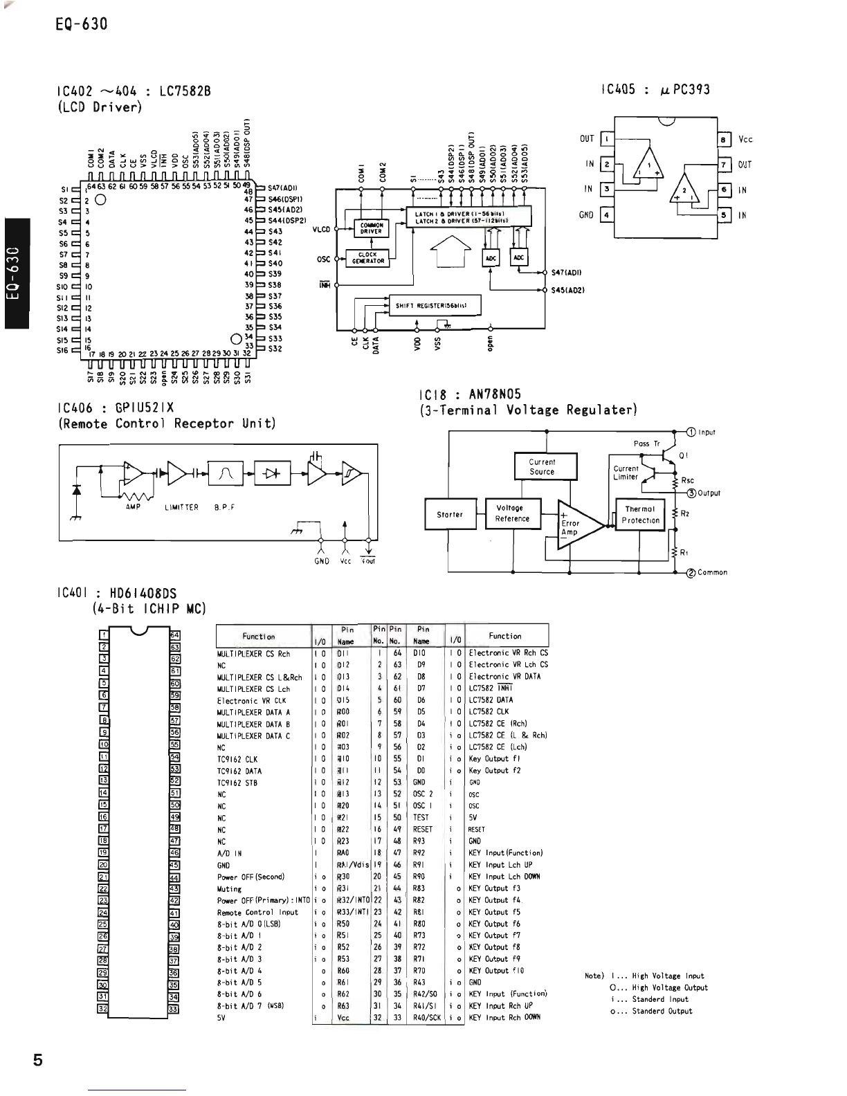
IC
BLOCK
..........................•.
4--5
DISPLAY
PIN
CONNECTIONS
6
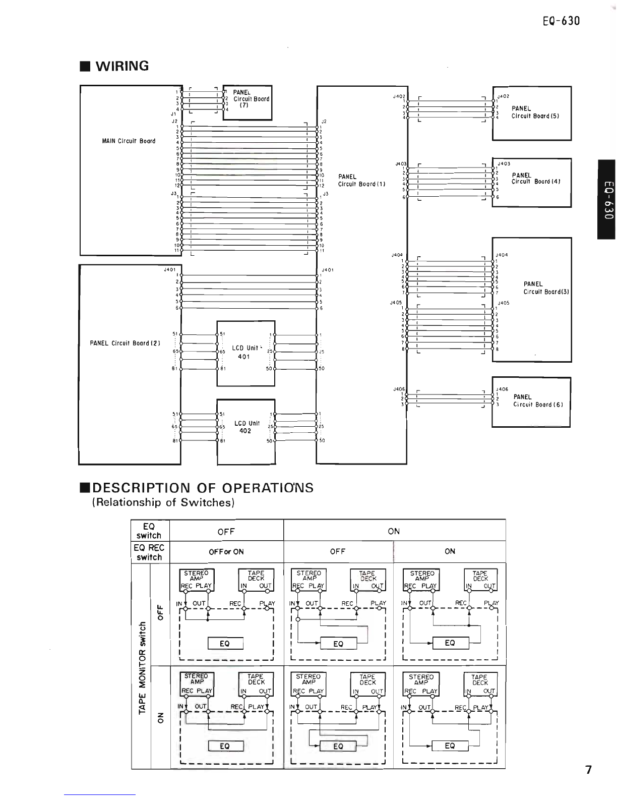
WI
RING
•....•..........................
7
DISCRIPTIPN
OF
OPERATIONS
7
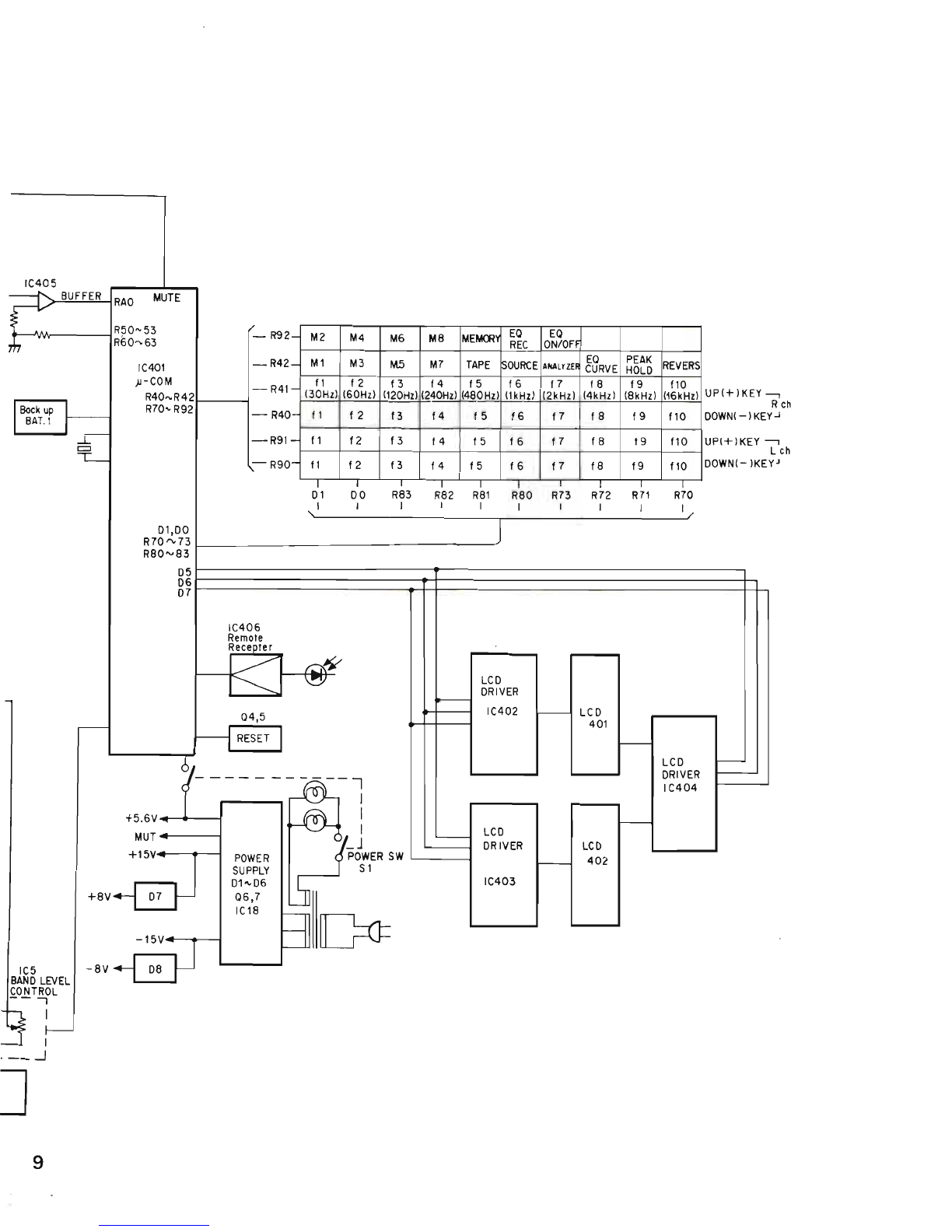
BLOCK
0I
AGRAM
......................•.
8,
q
PR
I
NTED
CI
RCU
IT
BOARD
10
--13
SCHEMATIC
DIAGRAM
......•...........
14.15
PARTS
LIST
16--20
}1002631
YAMAHA
YAMAHA
CORPORATION
HAMAMATSU,
JAPAN
3.7k-142
~~Printed
in
Japan
'89.5