Zarlink Le51HE0060V2 User manual

Le51HE0060V2
Le58QL063 QLSLAC™ /
Le5711/12 DSLIC™
Evaluation Board User’s Guide
Rev. A, Ver. 2
October 2, 2007
Document Number: 081167

www.zarlink.com
Information re lating to p roducts a nd services f urnished herein by Z arlink Se miconductor I nc. or i ts su bsidiaries (c ollectively “Zarlink”) is b elieved t o be rel iable.
However, Zarlink a ssumes n o liability f or errors t hat may a ppear in t his pu blication, or f or lia bility o therwise a rising from t he ap plication or use of a ny such
information, product or service or for any infringement of patents or other intellectual property rights owned by third parties which may result from such application or
use. Neither the supply of s uch information or pu rchase of product or se rvice con veys any li cense, ei ther express o r imp lied, u nder patents or o ther intellectual
property rights owned by Z arlink o r licensed from third parties by Z arlink, whatsoever. Purchasers of products are a lso hereby notified that the use of product in
certain ways or in combination with Zarlink, or non-Zarlink furnished goods or services may infringe patents or other intellectual property rights owned by Zarlink.
This publication is issued to provide information only and (unless agreed by Zarlink in writing) may not be used, applied or reproduced for any purpose nor form part
of any order or contract nor to be regarded as a representation relating to the products or services concerned. The products, their specifications, services and other
information ap pearing in this publication are sub ject t o cha nge by Za rlink without no tice. No wa rranty or gu arantee express or implied i s ma de re garding the
capability, performance or suitability of any product or service. Information concerning possible methods of use is provided as a guide only and does not constitute
any guarantee that such methods of use will be satisfactory in a specific piece of equipment. It is the user’s responsibility to fully determine the performance and
suitability of any equipment using such information and to ensure that any publication or data used is up to date and has not been superseded. Manufacturing does
not necessarily include testing of all functions or parameters. These products are not suitable for use in any medical products whose failure to perform may result in
significant injury or death to the user. All products and materials are sold and services provided subject to Zarlink’s conditions of sale which are available on request.
Purchase of Zarlink’s I2C components conveys a lic ense under the Philips I2C Patent rights to use these components in an I2C System, provided that the system
conforms to the I2C Standard Specification as defined by Philips.
Zarlink, ZL , th e Za rlink Se miconductor lo go an d th e L egerity l ogo an d co mbinations the reof, V oiceEdge, VoicePort, SLAC , ISLI C, ISLAC an d V oicePath are
trademarks of Zarlink Semiconductor Inc.
TECHNICAL DOCUMENTATION - NOT FOR RESALE
For more information about all Zarlink products
visit our Web Site at

i
Zarlink Semiconductor Inc.
Document ID# 081167 Date: Oct 2, 2007
Rev: AVersion: 2
Distribution: Public Document
TABLE OF CONTENTS
CHAPTER 1 INTRODUCTION . . . . . . . . . . . . . . . . . . . . . . . . . . . . . . . . . . . . . . . . . . . . . . . . . . . . . . . . . . . . . . 1
1.1 Overview . . . . . . . . . . . . . . . . . . . . . . . . . . . . . . . . . . . . . . . . . . . . . . . . . . . . . . . . . . . . . . . 1
1.2 DSLIC™ eTQFP (Exposed Pad) . . . . . . . . . . . . . . . . . . . . . . . . . . . . . . . . . . . . . . . . . . . . . 1
CHAPTER 2 BOARD SETUP AND CONNECTION . . . . . . . . . . . . . . . . . . . . . . . . . . . . . . . . . . . . . . . . . . . . . . 3
2.1 Board Features. . . . . . . . . . . . . . . . . . . . . . . . . . . . . . . . . . . . . . . . . . . . . . . . . . . . . . . . . . . 3
2.2 Board Connections. . . . . . . . . . . . . . . . . . . . . . . . . . . . . . . . . . . . . . . . . . . . . . . . . . . . . . . . 4
2.2.1 Power . . . . . . . . . . . . . . . . . . . . . . . . . . . . . . . . . . . . . . . . . . . . . . . . . . . . . . . . . . . 4
2.2.2 Telephone Line Interface. . . . . . . . . . . . . . . . . . . . . . . . . . . . . . . . . . . . . . . . . . . . . 4
2.3 Interconnection of the Le51HE0060V2 Evaluation Board . . . . . . . . . . . . . . . . . . . . . . . . . . 5
2.4 PCM/MPI Connections . . . . . . . . . . . . . . . . . . . . . . . . . . . . . . . . . . . . . . . . . . . . . . . . . . . . . 6
CHAPTER 3 BOARD OPERATION . . . . . . . . . . . . . . . . . . . . . . . . . . . . . . . . . . . . . . . . . . . . . . . . . . . . . . . . . . 7
3.1 Jumper Locations . . . . . . . . . . . . . . . . . . . . . . . . . . . . . . . . . . . . . . . . . . . . . . . . . . . . . . . . . 7
3.2 Jumper And Switch Settings For The Le51HE0060V2 Evaluation Board . . . . . . . . . . . . . . 8
CHAPTER 4 SOFTWARE OPERATION . . . . . . . . . . . . . . . . . . . . . . . . . . . . . . . . . . . . . . . . . . . . . . . . . . . . . 13
4.1 Overview . . . . . . . . . . . . . . . . . . . . . . . . . . . . . . . . . . . . . . . . . . . . . . . . . . . . . . . . . . . . . . 13
CHAPTER 5 SCHEMATICS . . . . . . . . . . . . . . . . . . . . . . . . . . . . . . . . . . . . . . . . . . . . . . . . . . . . . . . . . . . . . . . 15
5.1 Evaluation Board Schematics . . . . . . . . . . . . . . . . . . . . . . . . . . . . . . . . . . . . . . . . . . . . . . 15
4.2 Le51HE00602V Bill of Materials . . . . . . . . . . . . . . . . . . . . . . . . . . . . . . . . . . . . . . . . . . . . 23
CHAPTER 6 GLOSSARY . . . . . . . . . . . . . . . . . . . . . . . . . . . . . . . . . . . . . . . . . . . . . . . . . . . . . . . . . . . . . . . . . 27

Le51HE0060V2 Eval Board User Guide
ii
Zarlink Semiconductor Inc.

CHAPTER
1
Zarlink Semiconductor Inc.
1INTRODUCTION
1.1 OVERVIEW
The Zarlink Le51HE0060V2 evaluation board provides a platform to evaluate the capabilities of
the Le58QL063 QLSLAC™ and Le5711/12 DSLIC™ devices. All digital control signals, voice band
and MPI signals have test points for easy probing. Power is brought to the board via a set of banana
jack connectors. The QLSLAC device and the two DSLIC devices are mounted in ZIF sockets.
Detailed device explanations, operational circuit descriptions and required formulas can be found
within the individual QLSLAC and DSLIC device data sheets. Figure 1–1 shows the physical layout
of the Le51HE0060V evaluation board. Figure 1–2 shows a block diagram.
Figure 1–1 Le51HE0060V2 Evaluation Board
1.2 DSLIC™ eTQFP (Exposed Pad)
The Le5711/12 DSLIC device has an exposed thermal pad (heat slug) on the underside of the
device. This pad should be connected to VBAT for thermal relief (see the Thermal Design for
Le5711 and Le5712 application note for details of the connection). However, due to the type of
sockets used the connection to VBAT could not be made. Because of the socket, thermal
performance may be compromised. Do not connect to any other voltage.

Le51HE0060V2 Eval Board User Guide
2
Zarlink Semiconductor Inc.
Figure 1–2 Le51HE0060V2 Evaluation Board Block Diagram
QSLAC
DSLIC
DSLIC
Channel
1
Interface
(EMR)
Channel
2
Interface
(EMR)
Channel
3
Interface
(LCAS)
Channel
4
Interface
(LCAS)
Ringing Voltage
Distribution
Circuits
Power Distribution and Filtering
PCM/MPI Interface
Tip/Ring 1
Tip/Ring 2
Tip/Ring 3
Tip/Ring 4
To all circuits
VBAT1,
VBAT2,
BGND, +5 V, AGND
+3.3 V, DGND
Ringing Voltage
Ringing Rtn
Manual DSLIC
Controls

CHAPTER
3
Zarlink Semiconductor Inc.
2BOARD SETUP AND CON-
NECTION
2.1 BOARD FEATURES
The Le51HE0060V2 evaluation board design features the following:
• MPI/PCM Connector
• TIP/RING banana jacks and RJ-11 connectors
• Test Points for all major signals
• Banana jacks for all power connections
• QSLAC or manual control of DSLIC devices
• Two channels of solid state ringing switches and two channels of EMR ringing switches
• Battery or earth backed ringing
• Socketed components for easier evaluation
• On-board protection for tip/ring
• Meter rejection filtering
• DC parameters programmable via easy to change socketed components
• AC parameters programmable through the QLSLAC device

Le51HE0060V2 Eval Board User Guide
4
Zarlink Semiconductor Inc.
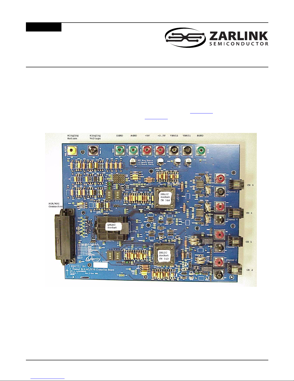
2.2 BOARD CONNECTIONS
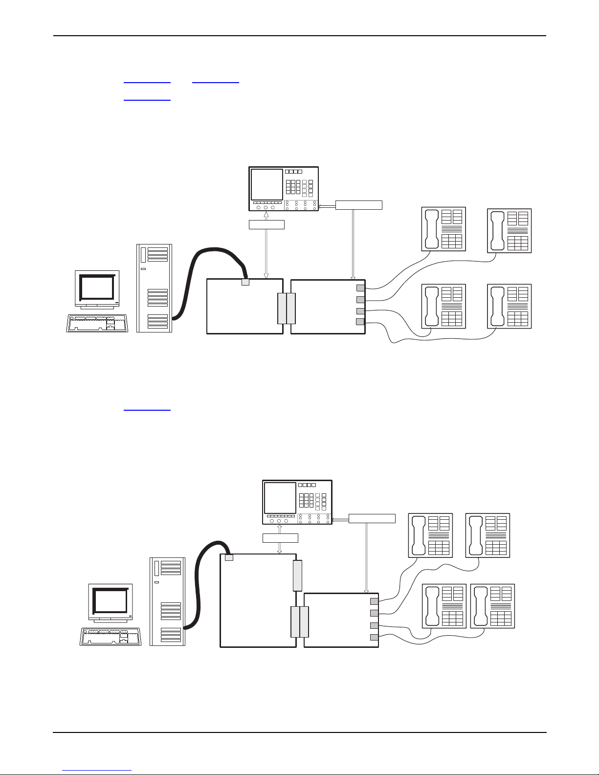
The Le51HE0060V2 can be plugged directly into either a Voice Path Demo (VP Demo) Board or an
Advanced Computer Interface Board (ACIF2-A) via the 50-pin IFB01 connector of the
Le51HE0060V2 evaluation board. All power is supplied via the nine banana jacks across the top of
the board. est points are included for all major signals. Eight banana jacks, labeled TIPXand
RINGX, are located on the right-hand edge of the evaluation board for connection to test equipment
or for connecting to a standard telephone station set. These jacks are also connected in parallel
with an industry standard RJ-11 connector.
2.2.1 Power
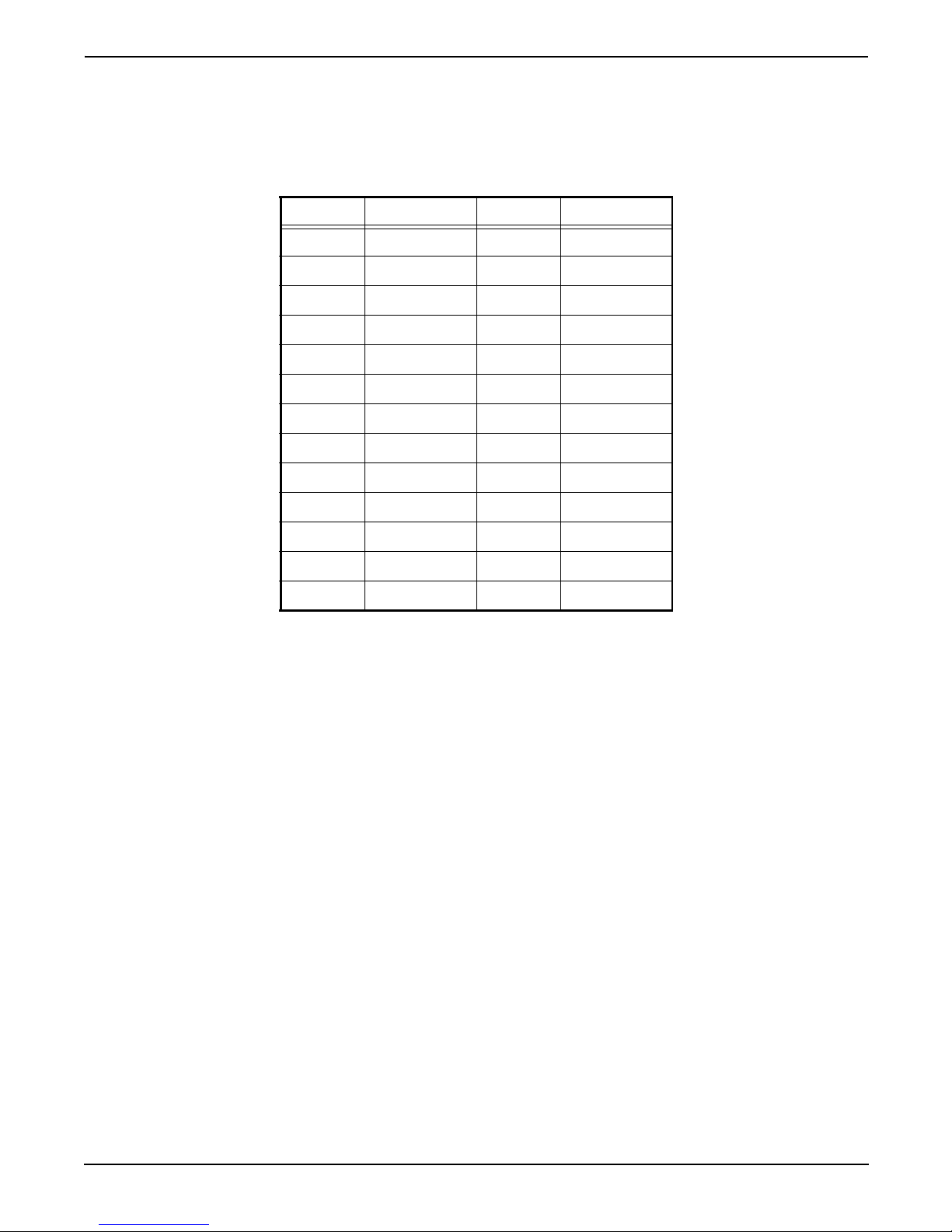
The required power for the board is supplied through nine banana jacks, as detailed in Table 2–1.
Table 2-1 Power Connections
Before connecting a ringing supply, the user should assure that the jumpers used for earth/battery
backed ringing selection are appropriately set. Details are contained in Chapter 3
Power sequencing is recommended, though not required. The suggested power sequencing
scheme is: VBAT1 powered-up first, followed by VBAT2, +3.3 V, and finally the +5-V supply. DGND
and AGND are tied together on the board with zero ohm resistors R9 and R10. BGND is not tied to
either AGND or DGND and care is required to assure that the maximum potential difference
between these points, as defined in the DSLIC data sheet, is not exceeded
2.2.2 Telephone Line Interface
To interface the Le51HE0060V2 evaluation board to a telephone station set, plug the telephone
station set into the TIP and RING banana jack pair (BJ1 and BJ2, BJ3 and BJ4, BJ12 and BJ13 or
BJ14 and BJ15). Alternately, the RJ-11 jacks (J11, J12, J13, J14) can be used.
A tip/ring surge protection circuit is included on the board. The LCAS protection circuits use a fixed
voltage protection scheme while the EMR protection circuits use a battery referenced protection
scheme.
Jack # Signal Description Board Name (PW1)
BJ5 VBAT1 Battery Supply, higher absolute voltage VBAT1
BJ6 VBAT2 Battery Supply, lower absolute voltage VBAT2
BJ7 +5 V Five volt analog supply Vcc
BJ8 +3.3 V 3.3-V digital supply 3.3 V
BJ9 DGND Digital ground, return for the +3.3-V supply DGND
BJ10 AGND Analog ground, return for the +5-V supply. AGND
BJ11 BGND Battery ground BGND
BJ16 Ring In Ringing voltage source Ring in
BJ17 Ring Return Ringing voltage return Ring return

Le51HE0060V2 Eval Board User Guide
5
Zarlink Semiconductor Inc.
2.3 INTERCONNECTION OF THE Le51HE0060V2 EVALUATION BOARD
A representative connection of a complete Zarlink evaluation platform setup is shown in
Figure 2–1 and Figure 2–2 below.
Figure 2–1 shows the evaluation board connected to the 50-pin connector (SPA) of the VP Demo
board. The host PC runs the VP-Script Software. Commands are passed through the VP Demo
board, via a serial COM port, to the evaluation board.
Figure 2–1 Le51HE0060V2 Evaluation Board to VP Demo Board Connection Diagram
Analog access to test equipment is connected to the TIP/RING connectors of the Le51HE0060V2
evaluation board. Digital PCM access to test equipment is provided through the VP Demo Board.
Figure 2–2 shows the evaluation board connected to the 50-pin connector LNB#0 of the ACIF2-A
Board. The host PC runs the WinACIF Software. Commands are passed through the ACIF2-A
board, via a serial COM port, to the evaluation board.
Figure 2–2 Le51HE0060V2 Evaluation Board to ACIF2-A Connection Diagram
Analog access to test equipment is connected to the TIP/RING connectors of the L371HE0060V2
evaluation board. Digital PCM access to test equipment is provided through the ACIF2-A Board.
VP Demo
Board QLSLAC
Le5711/12
PCM-4
Analog
Telephone Telephone
T1/E1
Telephone Telephone
ACIF2-A
Board QLSLAC
Le5711/12
PCM-4
Digital
Analog
Telephone Telephone
Telephone Telephone

Le51HE0060V2 Eval Board User Guide
6
Zarlink Semiconductor Inc.
2.4 PCM/MPI CONNECTIONS
All PCM/MPI interface signals are passed through the ACIF connector. Pinout for the VP Demo
Board SPA connector is shown below.
The QLSLAC device multiplexes Data In and Data Out on the same pin, DIO. To assure the VP-
Script Software will look for Data In and Data Out on the same pin, after starting the VP-Script
program, the user will need to open the PCM sub-menu and set chip select to CS11 and DIO to
combined.
Table 2–1 PCM/MPI Connections
Pin # Signal Pin # Signal
1 RST 26 Digital Ground
2 MCLK 27 Digital Ground
3 DCLK 28 Digital Ground
4 DRB 29 Digital Ground
5 DIO 30 Digital Ground
6 INT 31 Digital Ground
7 DXA 32 Digital Ground
8 CS 33 Digital Ground
9 DRA 34 Digital Ground
10 DXB 35 Digital Ground
11 FS 36 Digital Ground
12 PCLK 37 Digital Ground
13-25 N/C 38-50 Digital Ground

CHAPTER
7
Zarlink Semiconductor Inc.
3BOARD OPERATION
3.1 JUMPER LOCATIONS
Figure 3–1 Jumper Locations
DSLIC JumpersRinging JumpersDSLIC Manual
Controls

Le51HE0060V2 Eval Board User Guide
8
Zarlink Semiconductor Inc.
3.2 JUMPER AND SWITCH SETTINGS FOR THE Le51HE0060V2 EVALUATION
BOARD
This evaluation board contains a plethora of jumper and switch settings to allow testing of all the
operational modes of the QLSLAC/DSLIC combination. Figure 3–1 shows the mechanical position
of the jumpers and switches. All these settings may be categorized into several groups by logical
function, as follows:
1. QLSLAC controls
2. DSLIC controls (these are in the form of DIP switches instead of jumpers)
3. Line side options for DSLIC
4. Ringing options.
Table 3–1 QLSLAC Control Jumpers
Jumper Designation
1 to 2
jumpered
2 to 3
jumpered No jumper
JMCKE1
Select MCLK1 on IFB0
connector for QLSLAC
MCLK(E1) input
Tie QLSLAC MCLK(E1) to
DSLIC pin 18 with a pullup
resistor. Use this setting only
if the QSLAC is a mode that
uses this pin as an output.
QLSLAC MCLK input floats,
not recommended.
J3, LCAS control TSD input to LCAS for
channel 3 is open.
TSD input for channel 3 is
connected to DSLAC control
lead C73, DSLAC controls
LCAS for channel 3.
TSD input to LCAS for
channel 3 is open.
J4, LCAS control TSD input to LCAS for
channel 4 is open.
TSD input for channel 3 is
connected to DSLIC control
lead C74, DSLIC controls
LCAS for channel 4.
TSD input to LCAS for
channel 4 is open.
Table 3–2 DSLIC Switch Controls for Channel 1
Switch Designation
+ (logic one) setting
(position 2)
O (open) setting (position
1)
- (logic zero) setting
Position 0
S1-1
DSLIC channel 1 lead C11
tied to VCC (manual control
of DSLIC)
DSLIC channel 1 lead C11
tied to QSLAC lead C31
(QSLAC controls DSLIC)
DSLIC channel 1 lead C11
tied to AGND (manual
control of DSLIC)
S1-2
DSLIC channel 1 lead C21
tied to VCC (manual control
of DSLIC)
DSLIC channel 1 lead C21
tied to QSLAC lead C41
(QSLAC controls DSLIC)
DSLIC channel 1 lead C21
tied to AGND (manual
control of DSLIC)
S1-3
DSLIC channel 1 lead C31
tied to VCC (manual control
of DSLIC)
DSLIC channel 1 lead C31
tied to QSLAC lead C51
(QSLAC controls DSLIC)
DSLIC channel 1 lead C31
tied to AGND (manual
control of DSLIC)
S1-4 Not Used Not Used Not Used

Le51HE0060V2 Eval Board User Guide
9
Zarlink Semiconductor Inc.
Note:
The "open" position of the switch allows the QLSLAC device to control the three DSLIC channel controls. The
other two positions provide manual control. When using manual controls, refer to the DSLIC data sheet for
state information.
Table 3–3 DSLIC Switch Controls for Channel 2
Switch Designation
+ (logic one) setting
(position 2)
O (open) setting (position
1)
- (logic zero) setting
Position 0
S2-1
DSLIC channel 2 lead C12
tied to VCC (manual control
of DSLIC)
DSLIC channel 2 lead C11
tied to QSLAC lead C32
(QSLAC controls DSLIC)
DSLIC channel 2 lead C12
tied to AGND (manual
control of DSLIC)
s2-2
DSLIC channel 2 lead C22
tied to VCC (manual control
of DSLIC)
DSLIC channel 2 lead C21
tied to QSLAC lead C42
(QSLAC controls DSLIC)
DSLIC channel 2 lead C22
tied to AGND (manual
control of DSLIC)
S2-3
DSLIC channel 2 lead C32
tied to VCC (manual control
of DSLIC)
DSLIC channel 2 lead C31
tied to QSLAC lead C52
(QSLAC controls DSLIC)
DSLIC channel 2 lead C32
tied to AGND (manual
control of DSLIC)
S2-4 Not Used Not Used Not Used
Table 3–4 DSLIC Switch Controls for Channel 3
Switch Designation
+ (logic one) setting
(position 2)
O (open) setting (position
1)
- (logic zero) setting
Position 0
S3-1
DSLIC channel 3 lead C11
tied to VCC (manual control
of DSLIC)
DSLIC channel 3 lead C11
tied to QSLAC lead C33
(QSLAC controls DSLIC)
DSLIC channel 3 lead C11
tied to AGND (manual
control of DSLIC)
S3-2
DSLIC channel 3 lead C21
tied to VCC (manual control
of DSLIC)
DSLIC channel 3 lead C21
tied to QSLAC lead C43
(QSLAC controls DSLIC)
DSLIC channel 3 lead C21
tied to AGND (manual
control of DSLIC)
S3-3
DSLIC channel 3 lead C31
tied to VCC (manual control
of DSLIC)
DSLIC channel 3 lead C31
tied to QSLAC lead C53
(QSLAC controls DSLIC)
DSLIC channel 3 lead C31
tied to AGND (manual
control of DSLIC)
S3-4 Not Used Not Used Not Used
Table 3–5 DSLIC Switch Controls for Channel 4
Switch Designation
+ (logic one) setting
(position 2)
O (open) setting (position
1)
- (logic zero) setting
Position 0
S4-1
DSLIC channel 4 lead C12
tied to VCC (manual control
of DSLIC)
DSLIC channel 2 lead C11
tied to QSLAC lead C34
(QSLAC controls DSLIC)
DSLIC channel 4 lead C12
tied to AGND (manual
control of DSLIC)
S4-2
DSLIC channel 4 lead C22
tied to VCC (manual control
of DSLIC)
DSLIC channel 2 lead C21
tied to QSLAC lead C44
(QSLAC controls DSLIC)
DSLIC channel 4 lead C22
tied to AGND (manual
control of DSLIC)
S4-3
DSLIC channel 4 lead C32
tied to VCC (manual control
of DSLIC)
DSLIC channel 2 lead C31
tied to QSLAC lead C54
(QSLAC controls DSLIC)
DSLIC channel 4 lead C32
tied to AGND (manual
control of DSLIC)
S4-4 Not Used Not Used Not Used

Le51HE0060V2 Eval Board User Guide
10
Zarlink Semiconductor Inc.
Table 3–6 Line Side DSLIC Controls
Jumper Designation
1 to 2
jumpered
2 to 3
jumpered No jumper
J5, intended for
troubleshooting and
insertion of ammeter in line.
RING3 - LCAS and output
jacks connected to DSLIC N/A
RING3 LCAS and output
jacks not connected to
DSLIC
J6, intended for
troubleshooting and
insertion of ammeter in line.
TIP3 - LCAS and output
jacks connected to DSLIC N/A TIP3 LCAS and output jacks
not connected to DSLIC
J7, intended for
troubleshooting and
insertion of ammeter in line.
TIP4 - LCAS and output
jacks connected to DSLIC N/A TIP4 LCAS and output jacks
not connected to DSLIC
J8, intended for
troubleshooting and
insertion of ammeter in line.
RING4 - LCAS and output
jacks connected to DSLIC N/A
RING4 LCAS and output
jacks not connected to
DSLIC
J10, intended for insertion of
an ammeter
Connect VBAT (and
VBATREF) input of DSLIC
for channels 1 and 2 to
VBAT1 source.
N/A
Do not connect DSLIC VBAT
input to VBAT1 source. No
source is selected.
J15, intended for
troubleshooting and
insertion of ammeter in line.
TIP1 - ringing relay and
output jacks connected to
DSLIC
N/A
TIP1 ringing relay and output
jacks not connected to
DSLIC
J16, intended for
troubleshooting and
insertion of ammeter in line.
RING1 - ringing relay and
output jacks connected to
DSLIC
N/A
RING1 ringing relay and
output jacks not connected
to DSLIC
J17, intended for
troubleshooting and
insertion of ammeter in line.
TIP2 - ringing relay and
output jacks connected to
DSLIC
N/A
TIP2 ringing relay and output
jacks not connected to
DSLIC
J18, intended for
troubleshooting and
insertion of ammeter in line.
RING2 - ringing relay and
output jacks connected to
DSLIC
N/A
RING2 ringing relay and
output jacks not connected
to DSLIC
J19, intended for insertion of
an ammeter
Connect VBAT (and
VBATREF) input of DSLIC
for channels 3 and 4 to
VBAT1 source.
N/A
Do not connect DSLIC VBAT
input to VBAT1 source. No
source is selected.
J101, VBAT2 connections
Connect VBAT2 source to
pin TMG1(VBAT2) of DSLIC
for channel 1.
Connect VBAT1 source to
pin TMG1(VBAT2) of DSLIC
for channel 1.
TMG1(VBAT2) input to
DSLIC is open.
J102,VBAT2 connections
Connect VBAT2 source to
pin TMG12(VBAT2) of
DSLIC for channel 2.
Connect VBAT1 source to
pin TMG2(VBAT2) of DSLIC
for channel 2.
TMG2(VBAT2) input to
DSLIC is open.
J103, reserved for future
use, do not jumper. Do not jumper. Do not jumper. Do not jumper.
J201, VBAT2 connections
Connect VBAT2 source to
pin TMG1(VBAT2) of DSLIC
for channel 3.
Connect VBAT1 source to
pin TMG1(VBAT2) of DSLIC
for channel 3.
TMG1(VBAT2) input to
DSLIC is open.
J202,VBAT2 connections
Connect VBAT2 source to
pin TMG12(VBAT2) of
DSLIC for channel 4.
Connect VBAT1 source to
pin TMG2(VBAT2) of DSLIC
for channel 4.
TMG2(VBAT2) input to
DSLIC is open.

Le51HE0060V2 Eval Board User Guide
11
Zarlink Semiconductor Inc.
Note:
All of the jumpers in the table below MUST be set consistently for proper operation. All jumpers must connect
positions 1 and 2 for battery-backed ringing OR connect 2 and 3 for earth-backed ringing. The setting of these
jumpers must be checked before applying the ringing voltage source to the board.
Table 3–7 Ringing Controls
Jumper Designation 1 to 2
jumpered
2 to 3
jumpered
No jumper
JSR1, RING IN selector. Select battery backed
ringing for all 4 channels.
Select earth backed ring-
ing for all 4 channels.
Disconnect all 4 circuits
from the RING IN source.
JSR2, RING RETURN
selector.
Select battery backed
ringing for all 4 channels.
Select earth backed ring-
ing for all 4 channels.
Disconnect all 4 circuits
from RING RETURN.
JSR3, DSLIC DAC (posi-
tive input for ring trip
comparator) control for
channels 1 and 2.
Select battery backed
ringing.
Select earth backed ring-
ing.
Disconnect signal.
JSR4, DSLIC DAC (posi-
tive input for ring trip
comparator) control for
channels 1 and 2.
Select battery backed
ringing.
Select earth backed ring-
ing.
Disconnect signal.
JSR5, DSLIC DAC (posi-
tive input for ring trip
comparator) control for
channels 1 and 2.
Select battery backed
ringing.
Select earth backed ring-
ing.
Disconnect signal.
JSR6, DSLIC DB1 (nega-
tive input for ring trip
comparator) control for
channel 1.
Select battery backed
ringing.
Select earth backed ring-
ing.
Disconnect signal.
JSR7, DSLIC DB2 (nega-
tive input for ring trip
comparator) control for
channel 2.
Select battery backed
ringing.
Select earth backed ring-
ing.
Disconnect signal.
JSR8, DSLIC DAC (posi-
tive input for ring trip
comparator) control for
channels 3 and 4.
Select battery backed
ringing.
Select earth backed ring-
ing.
Disconnect signal.
JSR9, DSLIC DAC (posi-
tive input for ring trip
comparator) control for
channels 3 and 4.
Select battery backed
ringing.
Select earth backed ring-
ing.
Disconnect signal.
JSR10, DSLIC DAC (pos-
itive input for ring trip
comparator) control for
channels 3 and 4.
Select battery backed
ringing.
Select earth backed ring-
ing.
Disconnect signal.
JSR11, DSLIC DB1 (neg-
ative input for ring trip
comparator) control for
channel 3.
Select battery backed
ringing.
Select earth backed ring-
ing.
Disconnect signal.

Le51HE0060V2 Eval Board User Guide
12
Zarlink Semiconductor Inc.
JSR12, DSLIC DB2 (neg-
ative input for ring trip
comparator) control for
channel 4.
Select battery backed
ringing.
Select earth backed ring-
ing.
Disconnect signal.
JSR13, Ringing indicator
control.
Illuminate battery backed
ringing indicator.
Illuminate earth backed
ringing indicator.
Both indicators are off.
JRSR1, Select ring side
ringing source for chan-
nel 1.
Select battery backed
ringing.
Select earth backed ring-
ing.
Disconnect signal.
JRSR2, Select ring side
ringing source for chan-
nel 2.
Select battery backed
ringing.
Select earth backed ring-
ing.
Disconnect signal.
JRSR3, Select ring side
ringing source for chan-
nel 3.
Select battery backed
ringing.
Select earth backed ring-
ing.
Disconnect signal.
JRSR4, Select ring side
ringing source for chan-
nel 4.
Select battery backed
ringing.
Select earth backed ring-
ing.
Disconnect signal.
JRST1, Select tip side
ringing source for chan-
nel 1.
Select battery backed
ringing (ringing return via
RRTN1 resistor to
BGND).
Select earth backed ring-
ing.
Disconnect signal.
JRST2, Select tip side
ringing source for chan-
nel 2.
Select battery-backed
ringing (ringing return via
RRTN2 resistor to
BGND).
Select earth backed ring-
ing.
Disconnect signal.
JRST3, Select tip side
ringing source for chan-
nel 3.
Select battery-backed
ringing (ringing return via
RRTN3 resistor to
BGND).
Select earth backed ring-
ing.
Disconnect signal.
JRST4, Select tip side
ringing source for chan-
nel 4.
Select battery-backed
ringing (ringing return via
RRTN4 resistor to
BGND).
Select earth backed ring-
ing.
Disconnect signal.
Table 3–7 Ringing Controls
Jumper Designation 1 to 2
jumpered
2 to 3
jumpered
No jumper

CHAPTER
13
Zarlink Semiconductor Inc.
4SOFTWARE OPERATION
4.1 OVERVIEW
Three software platforms enable the user full control of the Le51HE0060V2 evaluation board. The
first two are control platforms to communicate with the evaluation board. The first platform is the VP
Demo Board and the VP-Script program or the Voice Path Mini-PBX software. The second platform
is the ACIF2-A hardware board along with its accompanying WinACIF2™ software program. The
third software program, WinSLAC2™, is used to calculate the required coefficients for the QLSLAC
and UVoSLIC devices.
The WinSLAC2 software models both the QLSLAC and Le9502 devices. The program is designed
to calculate programmable coefficients for optimizing two-wire impedance, hybrid balance and
transmit and receive responses. WinSLAC2 calculates and predicts transmission performance for:
• Two-Wire Return Loss
• Four-Wire Return Loss
• Transmit and receive attenuation distortion
• Transmit and receive path equalization
• Two-wire stability
For a more detailed description refer to the WinSLAC2 Software User's Guide, document
ID #080779.
The VoicePath Demo Board is one of the control platforms that can be used for communicating with
the evaluation board. The VP-Script program uses a command menu to send information to and
receive information from the evaluation board (supports PCM mode only). Refer to the VP-Script
Software User's Guide, publication #080757, for more detailed information.
Note:
The VP-Script program will need to be set up to send data to or receive data from the QLSLAC
device on a single pin. To do this, once the VP-Script program has been started, open the PCM sub-
menu and set chip select to CS11 and DIO to combined.
The ACIF2-A hardware board and the WinACIF software is an alternate platform that can be used
to communicate with the Le71He0062V board. Once the software has been initialized with the
correct configuration, a command menu is used to send information to and receive information from
the chip set (supports PCM and GCI modes). Refer to the WinACIF User's Guide, document
ID #080269, for more detailed information.
Note:
When the WinACIF program is initialized, the software is automatically set to transmit and receive
data on a single pin.

Le51HE0060V2 Eval Board User Guide
14
Zarlink Semiconductor Inc.

CHAPTER
15
Zarlink Semiconductor Inc.
5SCHEMATICS
5.1 EVALUATION BOARD SCHEMATICS
Schematics and a bill of materials for the Le51HE0060V2 evaluation board are included on the
following pages.

Le51HE0060V2 Eval Board User Guide
16
Zarlink Semiconductor Inc.
5
5
4
4
3
3
2
2
1
1
D D
C C
B B
A A
Page 1 Cover Sheet
Page 2 Block Schematic
Page 3 DSLIC 1 Schematic
Page 4 DSLIC 2 Schematic
Page 5 Power and Decoulping Schematic
Page 6 QSLAC Schematic
Page 7 Ring Signal Schematic
58QL063VC and 5712 Dual SLIC Evaluation Board
Revision 2.0
LE51HE0060V2 2.0ZaR
Zarlink QLSLAC DSLIC 5712 Evaluation Board
B
17Friday, June 20, 2003
WPE
PPC - VNA
2136 North 13th st
Reading, Pa 19604
Title
Size Document Number Rev
Date: Sheet of
Designer
Table of contents
Other Zarlink Motherboard manuals