Aerotech MXH Series User manual
Revision: 1.08.00
MXH Multiplier Board
Hardware Manual

Global Technical Support
Go to www.aerotech.com/global-technical-support for information and support about your Aerotech products. The website
provides downloadable resources (such as up-to-date software, product manuals, and Help files), training schedules, and
PC-to-PC remote technical support. You can also complete Product Return (RMA) forms and get information about repairs
and spare or replacement parts. For immediate help, contact a service office or your sales representative. Have your
customer order number available before you call or include it in your email.
United States (World Headquarters)
Phone: +1-412-967-6440
Fax: +1-412-967-6870
Email: service@aerotech.com
101 Zeta Drive
Pittsburgh, PA 15238-2811
www.aerotech.com
United Kingdom Japan
Phone: +44 (0)1256 855055
Fax: +44 (0)1256 855649
Email: service@aerotech.co.uk
Phone: +81 (0)50 5830 6814
Fax: +81 (0)43 306 3773
Email: service@aerotechkk.co.jp
Germany China
Phone: +49 (0)911 967 9370
Fax: +49 (0)911 967 93720
Email: service@aerotechgmbh.de
Phone: +86 (21) 3319 7715
Email: service@aerotech.com
France Taiwan
Phone: +33 2 37 21 87 65
Email: service@aerotech.co.uk
Phone: +886 (0)2 8751 6690
Email: service@aerotech.tw
This manual contains proprietary information and may not be reproduced, disclosed, or used in whole or in part without the
express written permission of Aerotech, Inc. Product names mentioned herein are used for identification purposes only and
may be trademarks of their respective companies.
Copyright © 1999-2017, Aerotech, Inc., All rights reserved.

Table of Contents MXH Multiplier Option Manual
Table of Contents
MXH Multiplier BoardHardware Manual 1
Table of Contents 3
List of Figures 4
List of Tables 5
EU Declaration of Conformity 7
Chapter 1: MXHMultiplier Board 9
1.1. Introduction 9
1.2. Multiplier Signals 11
1.3. Multiplier Board Setup 11
1.3.1. Oscilloscope 11
1.3.2. Equipment and Tools Required 11
1.3.3. Adjustment Procedure 12
1.4. Hardware Configurations 15
1.4.1. Fault Circuitry (JP1) (Rev A Only) 15
1.4.2. Marker Pulse Jumper (JP4) 15
1.4.3. Reset Circuitry (JP5) 15
1.4.4. Pulse Width Jumpers (JP2 and JP3) 16
1.4.5. Test Points 16
1.4.6. Connectors (J1 and J2) 17
1.4.7. Potentiometers 20
1.4.8. Output Options 20
1.5. Output Pulse Clock Speed 21
1.6. MXHMultiplier Board Specifications 23
1.6.1. Electrical Specifications 23
1.7. Dimensions 28
Chapter 2: MXHMultiplier Board (Rev A/Obsolete) 29
Appendix A: Warranty and Field Service 31
Appendix B: Revision History 33
Index 35
www.aerotech.com 3

4 www.aerotech.com
List of Figures
Figure 1-1: MXH Multiplier Board 9
Figure 1-2: MXH Multiplier Board Configuration 10
Figure 1-3: Plot of Input and Output Signals 11
Figure 1-4: Ideal Oscilloscope Displays (Sweep and Lissajou) 12
Figure 1-5: Not-Optimum Oscilloscope Lissajou Displays 13
Figure 1-6: MXH Multiplier Board Hardware Locations 14
Figure 1-7: MXH Encoder Cable Pinouts 19
Figure 1-8: 32 MHz Count Spacing 21
Figure 1-9: 16 MHz Count Spacing 22
Figure 1-10: 8 MHz Count Spacing 22
Figure 1-11: 4 MHz Count Spacing 22
Figure 1-12: MXH General Configuration (No Output Option Selected) 24
Figure 1-13: MXH Option -1 (Sine Differential Square Wave Output) 25
Figure 1-14: MXH Option -2 (Sine & Cosine Differential Square Wave Output) 26
Figure 1-15: MXH Option -3 (Sine, Cosine, and Marker Differential Square Wave Output) 27
Figure 1-16: MXH Multiplier Dimensions 28
Figure 2-1: MXH Multiplier Board Hardware Locations (REV A/Obsolete) 29
Figure 2-2: MXHMultiplier Dimensions (REVA/Obsolete) 30
MXH Multiplier Option Manual Table of Contents

Table of Contents MXH Multiplier Option Manual
List of Tables
Table 1-1: Order Option Summary 10
Table 1-2: Stage Table Verification Chart 14
Table 1-3: Settings for Pulse Width Jumpers 16
Table 1-4: MXH Multiplier Board Test Points 16
Table 1-5: Pinouts for Connector J1 17
Table 1-6: Pinouts for Connector J2 18
Table 1-7: MXHCable Options 18
Table 1-8: MXH Multiplier Board Potentiometers 20
Table 1-9: Digital Differential Factory Options 20
Table 1-10: MXH Multiplier Board Models and Specifications 23
Table 1-11: MXH Multiplier Board Electrical Specifications 23
www.aerotech.com 5

MXH Multiplier Option Manual Table of Contents
6 www.aerotech.com
This page intentionally left blank.

Declaration of Conformity MXH Multiplier Option Manual
EU Declaration of Conformity
Manufacturer
Aerotech, Inc.
Address
101 Zeta Drive
Pittsburgh, PA 15238-2811
USA
Product
MXH Encoder Multiplier Box
Model/Types
All
This is to certify that the aforementioned product is in accordance with the applicable requirements of the
following Directive(s):
2014/35/EU Low Voltage Directive LVD
2011/65/EU RoHS2 Directive
and has been designed to be in conformity with the applicable requirements of the following documents when
installed and used in accordance with the manufacturer’s supplied installation instructions.
EN 61010-1:2010 Safety requirements for electrical equipment
and furthermore declares that:
It is not allowed to put the equipment into service until the machinery into which it is to be incorporated or
of which it is to be a component has been found and declared to be in conformity with the provisions of
EU Directive 2006/42/EC and with national implementing legislation, i.e. as a whole, including the
equipment referred to in this Declaration.
Authorized Representative:
Simon Smith, European Director
Address:
Aerotech Ltd
The Old Brick Kiln
Ramsdell
Tadley
Hampshire
RG26 5PR
UK
Name
/ Alex Weibel
Position
Engineer Verifying Compliance
Location
Pittsburgh, PA
www.aerotech.com 7

MXH Multiplier Option Manual Declaration of Conformity
8 www.aerotech.com
This page intentionally left blank.
Introduction MXH Multiplier Option Manual
Chapter 1: MXHMultiplier Board
1.1. Introduction
Aerotech's MXH series multipliers are the ideal solution for high-resolution system requirements. The MXH
multiplier board is designed for use with rotary or linear sine wave encoders to increase encoder resolution.
The MXH series uses high-performance interpolation electronics to increase resolution by up to x2000.
The MXH model offers multiplication factors up to x2000. A linear encoder with a 4 µm grating period can
have resolution as fine as 2 nm.
Unlike most multiplication devices, the MXH doesn't sacrifice speed. A 32 MHz clock assures high speed
and high resolution. For example, with a resolution as fine as 8 nm, speeds of over 250 mm/s are achievable.
Aerotech's Dedication to the Science of Motion is reflected in some of the unique features of the MXH
series. Not only does the MXH boast industry-leading data rates, but for atypical resolution requirements,
Aerotech can create custom multiplication factors. This level of flexibility is unmatched by the competition
and is a result of our years of experience in the high-accuracy positioning market.
The MXH interface uses standard 25-pin D-type connectors, eliminating the need for expensive and hard to
find connectors. Limit switch and Hall-effect signals pass through the MXH, resulting in a more efficient
cabling scheme.
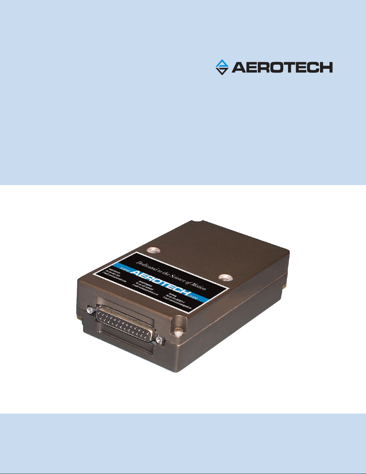
Figure 1-1: MXH Multiplier Board
www.aerotech.com Chapter 1 9
10 Chapter 1 www.aerotech.com
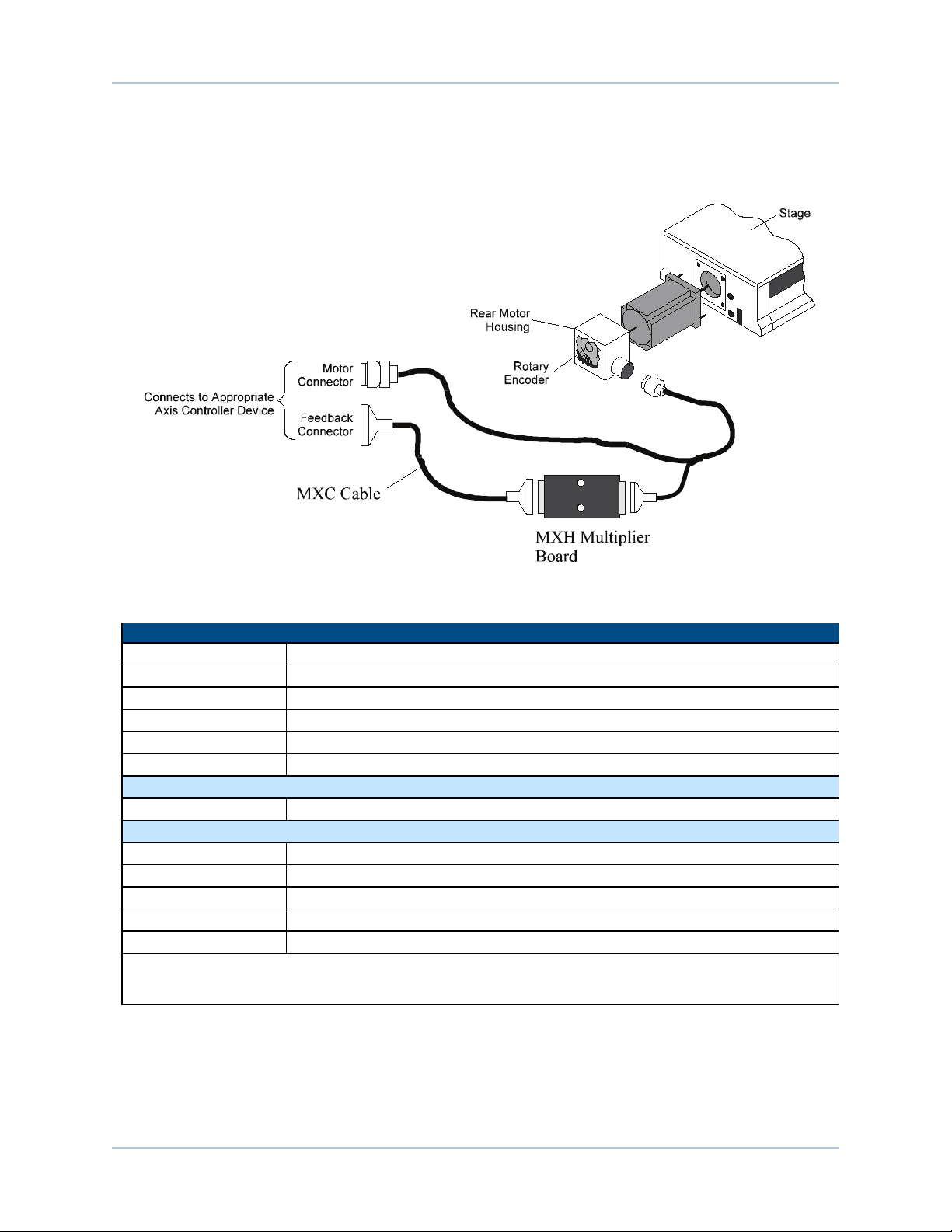
The MXH multiplier board connects between the encoder and the appropriate axis controller. Refer to Figure
1-2 for an example configuration. This connection does not affect Hall effect or limit signals; instead, it is a
simple add-in that uses mostly standard cables.
Figure 1-2: MXH Multiplier Board Configuration
Table 1-1: Order Option Summary
MXHSeries Multiplier
MXH50 External 50-times (net 200-times interpolation with quadrature) multiplier
MXH100 External 100-times (net 400-times interpolation with quadrature) multiplier
MXH200 External 200-times (net 800-times interpolation with quadrature) multiplier
MXH250 External 250-times (net 1000-times interpolation with quadrature) multiplier
MXH500 External 500-times (net 2000-times interpolation with quadrature) multiplier
MXHn-D External "n"-times custom resolution. Consult factory
Input Signal
D 1 Vpp input signal
Output Data Rate
2M 2 MHz output signal
4M 4 MHz output signal
8M 8 MHz output signal
16M 16 MHz output signal
32M 32 MHz output signal
Note: MXH multipliers are available in -A and -B versions as factory supplied configurations. Multiplication selections are possible in
0.25 increments up to MXH256, which multiplies into an integer after x4 (i.e. 0.25 or 0.5, 1.25, 33, etc. Unacceptable values are 1.7,
2.4, etc.). From MXH256 to MXH512, multiplication selections are possible in x1.0 increments.
MXH Multiplier Option Manual Introduction
Introduction MXH Multiplier Option Manual
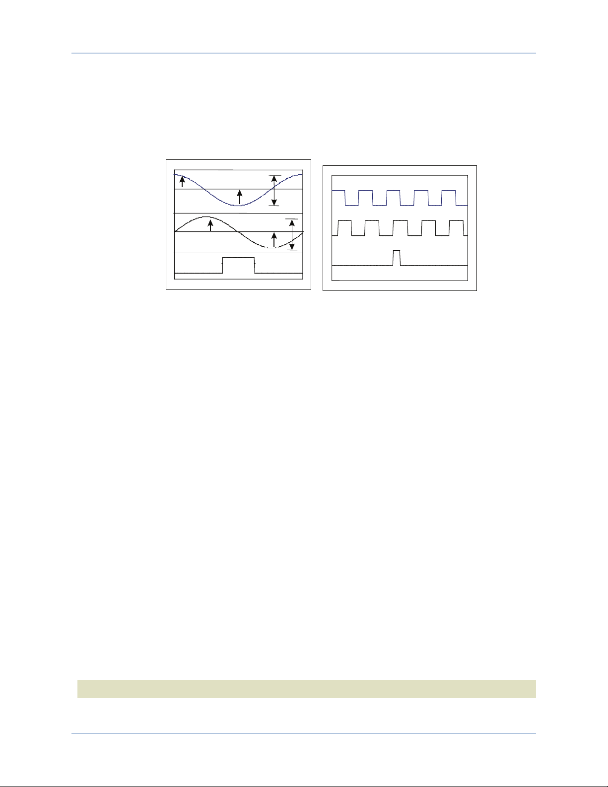
1.2. Multiplier Signals
The multiplier board accepts 1 V peak-to-peak voltage input signals. The outputs are square wave, RS-422
TTL compatible signals. The input marker signal is expected to be active high and located at the 255° point of
the 360° electrical cycle. The plots illustrated in Figure 1-3 show typical input and output signals (cosine,
sine, and marker).
INPUT SIGNALS
(After amplification on the MX board)
OUTPUT SIGNALS
COSINE
SINE
MARKER
TP10 - COSINE
Approx. Ref 2.5 V
0V
TP9 - SINE
Approx.
Ref 2.5 V
0V
TP6 - MARKER
1.9V
3.8Vpk-pk
3.8Vpk-pk
1.9V
1.9V
1.9V
Figure 1-3: Plot of Input and Output Signals
1.3. Multiplier Board Setup
The MXH Multiplier is designed to work with perfectly sinusoidal signals with no DC bias (offset). The actual
magnitude of the sine and cosine signals is not as important as the value of one signal relative to the other.
The MXH multiplier is a “ratio-metric” device, which means that the sine and cosine signals should be
adjusted for equal peak amplitudes. Any gain imbalance between the sine and cosine signals will result in
cyclic interpolation errors in the MXH output.
Any DC bias (offset) in sine or cosine will also cause cyclic interpolation errors in the multiplied output.
The gain and DC bias can be adjusted for each signal on the MXH multiplier circuit board.
1.3.1. Oscilloscope
Generally, systems operating at less than optimum performance due to interpolation errors will exhibit the
following symptoms:
1. A constant whining noise can be heard when running at low speeds.
2. At high speeds, a chirping noise can be heard when the table is accelerating and decelerating.
3. Using Aerotech’s application software as a diagnostic tool, a harmonic or a sub-harmonic of the
fundamental encoder frequency may be seen in the position error or velocity error plots of the axis
scope window.
1.3.2. Equipment and Tools Required
1. A two-channel oscilloscope capable of being isolated from ground and displaying a Lissajou pattern (X,
Y) of the sine and cosine encoder signals
2. Small slotted tip screwdriver or adjustment tool.
N O T E : The amplified signals can not exceed 4V peak-to-peak or a loss of accuracy occurs.
www.aerotech.com Chapter 1 11
12 Chapter 1 www.aerotech.com
1.3.3. Adjustment Procedure
1. Verify that oscilloscope is isolated from ground.
N O T E : An oscilloscope that is not isolated may cause permanent damage to the multiplier.
2. Connect signal common of scope to TP5 (2.5 VDC reference voltage), channel A scope probe to TP10
(COS-N), and channel B scope probe to TP9 (SIN-N). Refer to Figure 1-6 for MXH part locations.
3. Display encoder signals as a Lissajou pattern on the oscilloscope (x y mode).
4. Set channels A & B of the oscilloscope for 0.5 VDC per division, and zero the scope reference to the
center of the display.
5. Move table over the entire range of travel at a low speed, and verify that the peak to peak amplitude of
the circular pattern is between 2 to 3.9 Vp-p.
6. Move the table to the area where the amplitude is the largest, and verify or adjust for the following. (See
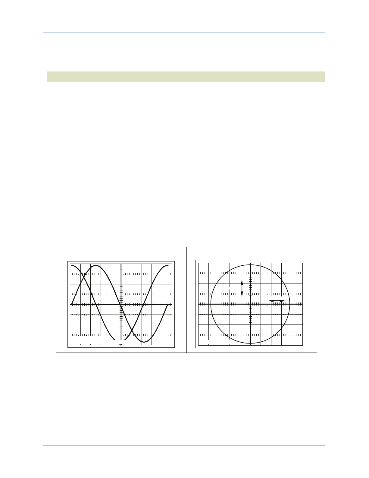
Diagram A – Diagram H in Figure 1-4 and Figure 1-5 for examples.)
i. COS-N gain is 3.8 Vp-p (+/- 0.1 Vp-p). Adjust R16 if necessary.
ii. COS-N DC offset is 0 VDC (+/- 0.1 VDC). Adjust R15 if necessary.
iii. SIN-N gain is equal to COS-N gain (+/- 0.1 Vp-p). Adjust R18 if necessary.
iv. SIN-N DC offset is 0 VDC (+/- 0.1 VDC). Adjust R17 if necessary.
v. Phase error is 0 degrees (+/- 4.5 Degrees). Adjust R14 if necessary.
vi. Repeat steps 6i through 6v.
7. Move table over the entire range of travel at a low speed and verify the following information in Table 1-
2.
Diagram A (Ideal)
SIN-N & COS-N Sweep Display No Phase, Gain or Offset Error
Diagram B (Ideal)
SIN-N & COS-N Lissajou Display No Phase, Gain, or Offset Error
COS-N
SIN-N
0.5 VOLT/DIVISION
0.1 MILLISECOND/DIVISION
0.5 VOLT/DIVISION
COS-N
SIN-N
Figure 1-4: Ideal Oscilloscope Displays (Sweep and Lissajou)
MXH Multiplier Option Manual Introduction
Introduction MXH Multiplier Option Manual
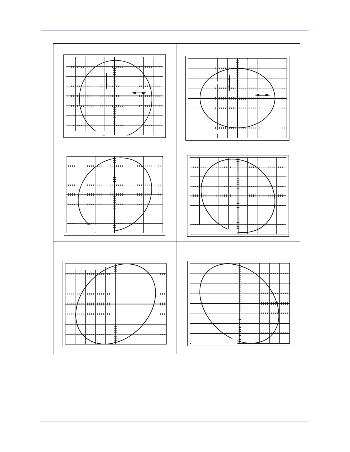
Diagram C (Not Optimum)
SIN-N & COS-N Lissajou Display DC Offset Error: SIN-N –0.1V, COS-N +0.1V
Diagram D (Not Optimum)
SIN-N & COS-N Lissajou Display Gain Error: SIN-N 3Vp-p, COS-N 3.8Vp-p
0.5 VOLT/DIVISION
SIN-N
COS-N
SIN-N
COS-N
0.5 VOLT/DIVISION
Diagram E (Not Optimum)
SIN-N & COS-N Lissajou Display Showing Phase Error of +4.5º
Diagram F (Not Optimum)
SIN-N & COS-N Lissajou Display Showing Phase Error of -4.5º
0.5 VOLT/DIVISION
4.5 DEGREE PHASE ERROR
0.5 VOLT/DIVISION
-4.5 DEGREE PHASE ERROR
Diagram G (Not Optimum)
SIN-N & COS-N Lissajou Display Showing Phase Error of + 9º
Diagram H (Not Optimum)
SIN-N & COS-N Lissajou Display Showing Phase Error of - 9º
+ 9 DEGREE PHASE ERROR
0.5 VOLT/DIVISION
0.5 VOLT/DIVISION
-9 DEGREE PHASE ERROR
Figure 1-5: Not-Optimum Oscilloscope Lissajou Displays
www.aerotech.com Chapter 1 13

14 Chapter 1 www.aerotech.com
Table 1-2: Stage Table Verification Chart
Lissajou Pattern Optimum Acceptable
Signal Amplitude 3 to 3.8 Vp-p 2 to 4.0 Vp-p
Gain Error ≤ 2.5% of Signal Amplitude (Vp-p) ≤ 5.0% of Signal Amplitude (Vp-p)
DC Offset Error ≤ 2.5% of Signal Amplitude (Vp-p) ≤ 5.0% of Signal Amplitude (Vp-p)
Phase Error ≤ 4.5 º ≤ 9.0 º
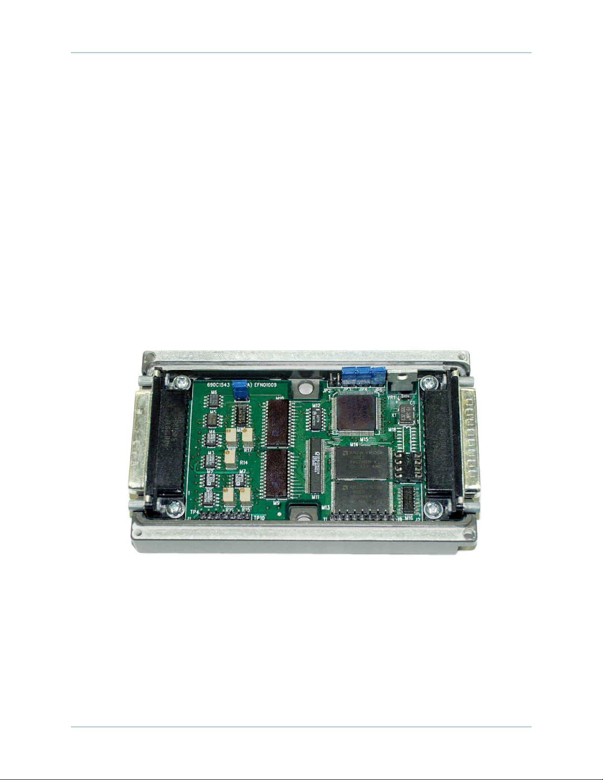
J3 F.S.
1
M11
M10
J1
Female
TP4
TP5
TP6
TP7
TP8
TP9
TP10
TP11
TP12
TP13
TP14
TP15
TP16
TP17
TP18
TP19
JP2
JP3
JP4
JP5
J2
Male
X1
32 MHz
1
VR1
EZ1086CT
C1
+
M17
1
M16
M15
R15
R16
R17
R18
R14
1
M14
26LS32
M13
M12
JP1
0 OHM
M19
XC17S30XL
M18
AM26LS32
M20
AM26LS32
1
690C1543 Rev. C
M7
M6
M5
M4
M3
M2
M1
M9
M8
Figure 1-6: MXH Multiplier Board Hardware Locations
MXH Multiplier Option Manual Introduction

Introduction MXH Multiplier Option Manual
1.4. Hardware Configurations
The amplified input signals at Test Points TP9 and TP10 (refer to Figure 1-6 for locations) should be
configured for normal 3.8 V peak-to-peak signals, see the explanation in Section 1.3. However, the multiplier
board has an acceptable range of amplified input signals from 2V peak-to-peak to 4V peak-to-peak.
The following sections discuss the hardware used to configure the MXH multiplier board. The hardware is
accessible by removing two screws securing the dust cover to the board.
1.4.1. Fault Circuitry (JP1) (Rev A Only)
The fault circuitry detects input signal magnitudes below 0.5 Volt peak-to-peak. If a fault is detected, all
outputs are set to a high impedance state. Fault detection is enabled with jumper JP1 in. Removing JP1
defeats fault detection. For jumper location, refer to Figure 1-6.
1.4.2. Marker Pulse Jumper (JP4)
The marker pulse jumper in the default setting of JP4 sets the pulse width to the minimum pulse width. In
this case, the marker is one output pulse wide and is qualified with the input marker. When JP4 is out, the
marker signal of the encoder is an output and is the same width as the input pulse and no qualification is
performed. For jumper location, refer to Figure 1-6.
1.4.3. Reset Circuitry (JP5)
The default setting (jumper in) of the reset circuitry jumper (JP5) resets the board if a fault is detected. The
faults that can occur are a loss of 5V, loss of clock signal, and low input signal magnitudes.
www.aerotech.com Chapter 1 15
16 Chapter 1 www.aerotech.com
1.4.4. Pulse Width Jumpers (JP2 and JP3)
Table 1-3: Settings for Pulse Width Jumpers
JP2 JP3 Function
1
1
Minimum pulse width = 0.03125 µs
Master clock frequency = 32 MHz
1
1
Minimum pulse width = 0.0625 µs (default)
Master clock frequency = 16 MHz (default)
1
1
Minimum pulse width = 0.125 µs
Master clock frequency = 8 MHz
1
1
Minimum pulse width = .25 µs
Master clock frequency = 4 MHz
1.4.5. Test Points
Table 1-4: MXH Multiplier Board Test Points
Test Points Function
TP4 Ground
TP5 Sin Reference (Approx. 2.5V)
TP6 Squared up marker signal from encoder
TP7 Cos reference (Approx. 2.5V)
TP8 NC
TP9 Amplified input sine wave (0 - 5V)
TP10 Amplified input cosine wave (0 - 5V)
TP11 A/D sample clock
TP12 HDC
TP13 LDC
TP14 M14 Flash reset
TP15 M13 Flash reset
TP16 Flash Ready/Busy signal
TP17 Output marker, square wave
TP18 Output sine, square wave
TP19 Output cosine, square wave
MXH Multiplier Option Manual Introduction
Introduction MXH Multiplier Option Manual
1.4.6. Connectors (J1 and J2)
There are two connectors on the MXH multiplier board; J1, which receives signals from a sinusoidal
encoder, and J2, that outputs the frequency-multiplied RS-422 pulses. The “multiplied” signals are then
taken to the controller through the breakout or interface boards. J1 is a 25-pin female “D” style connector. J2
is a 25-pin male “D” style connector. The pinouts for these connectors are listed in Table 1-5 and Table 1-6.
The MXH box only uses the SIN, COS, and Marker signals. Hall effect, Limit, and the rest of the signals are
passed directly through the MXH box with minor or no modification. As with any high frequency signal
transfer over cables, strict guidelines for interconnecting cables should be followed for noise-less, properly
phased signal delivery. Figure 1-7 is an illustration of the MXH encoder cable with the pinouts.
Table 1-5: Pinouts for Connector J1
Pin Signal Description
1 Shield Tied to motor ground. Grounded when connected to an interface board through
chassis and J2, pin 1.
2 Tied to J2-2
3 Encoder +5V Supplies 5V to encoder
4 Ground Analog ground. Supplies ground to encoder, tied up with J1, pins 20, 21.
5 Hall Effect B From motor, connected to J2, pin 5. 10K pull-up attached.
6 Marker - Analog sinusoidal input from encoder.
7 Marker + Analog sinusoidal input from encoder.
8Output option dependent (refer to Section 1.4.8. and Figure 1-12 through Figure 1-
15).
9Output option dependent (refer to Section 1.4.8. and Figure 1-12 through Figure 1-
15).
10 Hall Effect A From motor, directly connected to J2-10. 10K pull-up attached
11 Hall Effect C From motor, directly connected to J2-11. 10K pull-up attached
12 CW Limit From motor, directly connected to J2-12. 10K pull-up attached
13 Output option dependent (refer to Section 1.4.8. and Figure 1-12 through Figure 1-
15).
14 COS + Analog sinusoidal input from encoder.
15 COS - Analog sinusoidal input from encoder.
16 +5V Supplies 5V to encoder
17 SIN + Analog sinusoidal input from encoder.
18 SIN - Analog sinusoidal input from encoder.
19 Output option dependent (refer to Section 1.4.8. and Figure 1-12 through Figure 1-
15).
20 Ground Analog ground. Supplies ground to encoder, tied up with J1, pins 4, 21.
21 Ground Analog ground. Supplies ground to encoder, tied up with J1, pins 4, 20.
22 Home Limit Directly connected to J2, pin 22. 10K pull-up attached.
23 Output option dependent (refer to Section 1.4.8. and Figure 1-12 through Figure 1-
15).
24 CCW Limit Directly connected to J2, pin 24. 10K pull-up attached.
25 Output option dependent (refer to Section 1.4.8. and Figure 1-12 through Figure 1-
15).
www.aerotech.com Chapter 1 17
18 Chapter 1 www.aerotech.com
Table 1-6: Pinouts for Connector J2
Pin Signal Description
1 Shield Grounded when connected to an interface board.
2 Tied to J1-2
3 Encoder +5V Supplies 5V to motor encoder through J1, pin 3.
4 Ground Supplies ground to encoder, tied up with J2, pins 20, 21.
5 Hall Effect B Brings Hall signal directly from motor to interface board through J1, pin 5.
6 Marker - Multiplied RS-422 out from MXH to interface board.
7 Marker + Multiplied RS-422 out from MXH to interface board.
8Output option dependent (refer to Section 1.4.8. and Figure 1-12 through Figure 1-
15).
9Output option dependent (refer to Section 1.4.8. and Figure 1-12 through Figure 1-
15).
10 Hall Effect A Brings Hall signal directly from motor to interface board through J1, pin 10.
11 Hall Effect C Brings Hall signal directly from motor to interface board through J1, pin 11.
12 CW Limit Brings Hall signal directly from motor to interface board through J1, pin 12.
13 Output option dependent (refer to Section 1.4.8. and Figure 1-12 through Figure 1-
15).
14 COS + Multiplied RS-422 out from MXH to interface board.
15 COS - Multiplied RS-422 out from MXH to interface board.
16 +5V Supplies 5V from the interface board to MXH, tied to J1, pin 16.
17 SIN + Multiplied RS-422 out from MXH to interface board.
18 SIN - Multiplied RS-422 out from MXH to interface board.
19 Output option dependent (refer to Section 1.4.8. and Figure 1-12 through Figure 1-
15).
20 Ground Supplies ground to encoder, tied up with J2, pins 4, 21.
21 Ground Supplies ground to encoder, tied up with J2, pins 4, 20.
22 Home Limit Brings Home Limit directly from motor to interface board through J1, pin 22.
23 Output option dependent (refer to Section 1.4.8. and Figure 1-12 through Figure 1-
15).
24 CCW Limit Brings CCW Limit directly from motor to interface board through J1, pin 24.
25 Output option dependent (refer to Section 1.4.8. and Figure 1-12 through Figure 1-
15).
Table 1-7: MXHCable Options
Cable Description
MXC-xx MXH to controller cable
BFCMX-xx MXH to motor or controller cable
DC-DDMX-xx ADR to MX box feedback cable
DC-MSOMX-xx DC Brush Motor to MXH cable
PFCMX-xx MXH to (controller) flying lead cable
“xx” is the available length in feet
MXH Multiplier Option Manual Introduction

Introduction MXH Multiplier Option Manual
Note: Maximum Cable Length Is 10 Meters
Twisted Pairs Are 1-4 Turns / Inch
ENCODER
SHIELD TO CASE
SINE +
SINE –
COSINE +
COSINE –
MARKER –
MARKER +
+5V
COMMON
MX BOARD J1 (25 PIN MALE D)
SHIELD (CONNECTOR SHELL)
17 SINE +
18 SINE –
14 COSINE +
15 COSINE –
6 MARKER –
7 MARKER +
3 +5V
21 COMMON
20 COMMON
OUTER SHIELD
TWIST
TWIST
TWIST
TWIST
INNER SHIELD
Figure 1-7: MXH Encoder Cable Pinouts
www.aerotech.com Chapter 1 19
20 Chapter 1 www.aerotech.com
1.4.7. Potentiometers
For the location of the pots on the MXH multiplier board, refer to Figure 1-6.
Table 1-8: MXH Multiplier Board Potentiometers
Pot Function
R14 Phase adjust between sine and cosine signals
R15 Balance for encoder cosine signal
R16 Gain adjust for encoder cosine signal
R17 Balance for encoder sine signal
R18 Gain adjust for encoder sine signal
1.4.8. Output Options
The following Digital Differential factory options are available; refer to Figure 1-12,Figure 1-13,Figure 1-14,
and Figure 1-15. All four of these options provide RS-422 differential square wave output signals produced
after multiplication. Options 1-3 add additional outputs providing RS-422 signals from the un-multiplied input
signals
Table 1-9: Digital Differential Factory Options
Option Code Description
NONE Differential square wave sine / cosine multiplied signals (standard)
-1 Differential square wave output of un-multiplied sine signal
-2 Differential square wave output of un-multiplied sine and cosine signals
-3 Differential square wave output of un-multiplied sine, cosine and marker (unqualified)
signals.
MXH Multiplier Option Manual Introduction
Other manuals for MXH Series
1
This manual suits for next models
6
Table of contents
Other Aerotech Media Converter manuals

Popular Media Converter manuals by other brands

Patton electronics
Patton electronics 2072 Installation and operation manual

ADLINK Technology
ADLINK Technology PCI-8124 user manual

Hama
Hama 00083215 operating instructions

Sumake
Sumake ST-2275 Operator instructions

WebGate
WebGate SDI2HD instruction manual

SRS Lighting
SRS Lighting DSR10-3 instruction manual


