akira LCT-32CHSTP User manual

LCT TV
Service Manual

-2-
Model No.: LCT-32CHSTP
Version: 1.0
M
M
Mo
o
od
d
de
e
el
l
l:
:
:
L
L
LC
C
CT
T
T-
-
-3
3
32
2
2C
C
CH
H
HS
S
ST
T
TP
P
P
C
C
Ch
h
ha
a
as
s
ss
s
si
i
is
s
s:
:
:
L
L
LS
S
S-
-
-0
0
08
8
8

-3-
Model No.: LCT-32CHSTP
Version: 1.0
CONTENTS
MAIN FEATURE..................................................................................................................................... 4
MAIN ICS FUNCTION INTRODUCTION ............................................................................................ 8
SYMPTOMS AND CORRECTION ...................................................................................................... 46
LIST OF BREAKABLE AND MAINTENANCE PARTS .................................................................... 47
FACTORY MODE AND NOTICE ........................................................................................................ 49
CIRCUIT DIAGRAM ............................................................................................................................ 53
WIRING DIAGRAM ............................................................................................................................. 66
EXPLODED VIEW................................................................................................................................ 67
PART LIST ............................................................................................................................................. 68

-4-
Model No.: LCT-32CHSTP
Version: 1.0
MAIN FEATURES
Radio Frequency input; support CATV
Capable to receive the full-append cable programs in 470MHZ
SCART input/output
SCART1can input CVBS/RGB Video format, SCART2 can input CVBS Video format, both can
output TV signal
AV input
Capable to receive PAL, NTSC, SECAM color systems; Very convenient to watch VCR (video
cassette recorder), Pickup Camera, other Disc’s programs
Y/C component signal input (same to S-Video input)
Convenient to receive the Y/C high definition component signal from DVD
HDTV input
Capable to receive the high definition YPbPr signal in 480i, 480p, 576i, 720p, 1080i, and 1080p
formats
VGA input
Convenient to connect with the host computer
Capable to use as the display terminal
Connect the 3.5mm(diameter) audio cord to your computer’s audio main board, you can listening
the beautiful music transmitted from your host computer
DVI input
Convenient to receive DVI signal
Teletext decoder
PIP, POP, PBP function
Turn on with intelligence
Zoom mode
LTI, CTI, and black field
BBE sound technology
Trusurround sound technology
Full-light display
Picture amending display function
Super definition display panel
3:2, 2:2 Pull Down
TV program scan function
Timer function
Automatically on/off in certain preset time, and transmit automatically to the fixed channel
Blue background noise reduction
In TV, AV (S-Video), YCbCr, and YPbPr modes, screen displays soft blue background if there is
no signal input

-5-
Model No.: LCT-32CHSTP
Version: 1.0
Auto Off if no signal input
In TV mode, the LCD TV will automatically power off within 15 minutes and enter into the
Power Energy Saving Mode if there is no signal input.
Chinese/English menu
Ordinary and graphical user interface makes the menu operation more convenient and
intuitionistic
Power Energy Saving Mode (power management mode)
In PC mode, the LCD TV will automatically power off within 30 seconds and enter into the
Power Energy Saving Mode if there is no VGA signal input. It will automatically exit from the
Power Energy Saving Mode and work again when it received a valid VGA signal or press any
button on the panel/remote control.
Plug and Play
It is no need to equip any installation software when the product is used as computer terminal
display equipment
Legerity, convenience, low power consumption

-6-
Model No.: LCT-32CHSTP
Version: 1.0
Unit IC Compositions:
LS08 chassis LCD TV is mainly composed of regulator IC, RF IC, video processor IC, Power
Amplify IC, Analog Video IC, System Control IC and Key Control IC, see this IC frame as below:

-7-
Model No.: LCT-32CHSTP
Version: 1.0
PCB Assembly:
It is mainly composed of TV Board、Remote Control Receiver (Signal Receiver), K Board and Main
Board. Hereunder function introduction to every PCB Assembly:
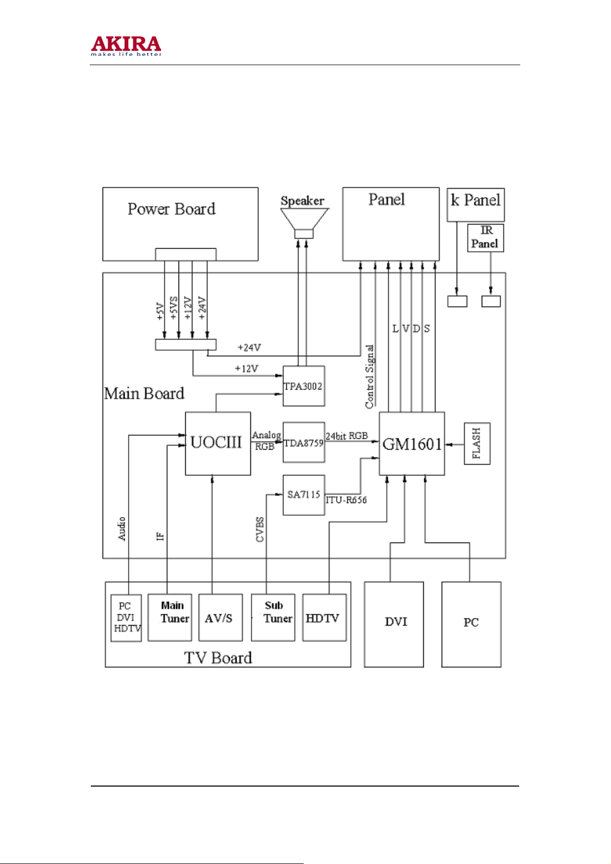
No. Parts Description
1 Main Board
Assembly
It is the core of signal processing for LCD TV, which takes responsibility
of transforming outer signal into the uniform digital signal identified by
LCD display with use of System Control IC TV and AV signals input from
TV Board are decoded by UOCIII to transport RGB signal which is to be
transformed by TDA8759 modulus to transport 24bit RGB digital signal,
then it is to be transformed by GM1601/GM1501 to produce LVDS signal
displayed on the screen, in addition, signals input from VGA, DVI
would directly enter into GM1501 procedure, format transformation and
on screen display.
2 TV Board
Assembly
It is mainly composed of two tuners (main and sub tuners), AV/S, HD
signal terminals and some peripheral processing IC. The main tuner
demodulates RF signal to IF signal, and the sub tuner produces CVBS
signal, all signals are sent to the main board after transfer.
3 Remote Control
Receiver
Assembly
It is composed of one indicator light and one remote control receiver,
which enable Users operate the TV conveniently and know its current
working status simply with a remote control.
4 Built-in Power
Board Assembly
It can transform AC 220V into DC for ICs, including +24V, +12V, +5V
and +5VS power supply in standby mode.
5 K Board
Assembly
It consists of 7 function buttons by which users can operate the TV freely.
6 Screen Assembly Screens for LS08 have built-in adverse transformer, which change DC to
high voltage AC signal lightening the back light; The LCD screen is used
to display the image after the image signal has been processed by the
main board.

-8-
Model No.: LCT-32CHSTP
Version: 1.0
MAIN ICS FUNCTION INTRODUCTION
GENERAL INTRODUCTION
TV Board
Number Location Type Main Function
1 UT1 TAD5-E2I22RW2 Audio and image intermediate frequency
signal output
2 UT2 TMD2-E49IPWA Sub picture CVBS signal output
Main Board
3 U302, U303 24LC21A T/SN EEPROM
4 U701 24LC32A T/SN Buffer
5 U306, U307,
UA3
FSAV330QSCX Switch selection
6 K201 K3953M Audio surface filter
7 K202 K9656M Audio surface filter
8 U6 TPA3002D2PHPR Audio amplifier
9 U801 AM29LV800DT-70EC
Flash,control program inside
10 U700 GM1501-BD Video processor
11 U201 TDA15021H/N1B07 AV decoder
12 U402 SAA7115HL/V1 Sub channel video decoder
13 U305 SM5302AS-G-ET High definition signal filter
14 U400 TDA8759HV/8/C1 Video signal modulus transformer
15 U5 TDA9178T/N1 Video signal picture amendment
16 U600 MT46V2M32LG-4 Frame buffer

-9-
Model No.: LCT-32CHSTP
Version: 1.0
ICs FUNCTION INTRODUCTION IN DETAILS
Main Tuner (TAD5-E2122RW2)
Pin Definition Description
1 AGC Auto gain control
2 UT NC
3 ADD Ground
4 SCL IIC bus (Clock)
5 SDA IIC bus (Data)
6 NC NC
7 +5V Power supply
8 NC NC
9 30V To produce 0~30V tune voltage
10 NC NC
11 IF Intermediate frequency TV signal
Intermediate frequency TV signal
Sub Tuner (TMD2-E49IPIWA):
Pin Definition Description
1 AGC Auto gain control
2 NC NC
3 ADD Ground
4 SCL IIC bus (Clock)
5 SDA IIC bus (Data)
6 NC NC
7 +5V Power supply
8 NC NC
9 33V To produce 0~30V tune voltage to 0~30V
10 NC NC
11 IF Intermediate frequency output (NC)
12 IF Intermediate frequency output (NC)
13 SW0 Band control
14 SW1 Band control
15 NC NC
16 SIF NC
17 AGC Auto gain control
18 VEDIO CVBS signal output
19 +5V Power supply
20 AUDIO NC

-10 -
Model No.: LCT-32CHSTP
Version: 1.0
GM1501
GM1501is a kind of processing chassis for dual channels image and video, which is mainly used for
LCD displays and integrative TV products. With the resolution of WUXGA, it not only supports PIP
technique, but possesses some IC functions applied to image catch, process and clock display. It
integrates high velocity AD converter, PLL, high reliability DVI receiver, X86 series mic control and
LCDS inverter. See the features as below:
Features
High quality image zoom function
Analog RGB signal input interface
Intelligent output signal auto identification
Integrated high-power PLL output
High-reliable self-adaptive DVI input interface
4:4:4/4:2:2/CCR656/601 8/16/24bit digital video interface
Embedded IC for adjustments of gain, contrast, brightness, color saturation, hue and flesh tone.
Efficiency in reducing EMI electromagnetism inference power consumption
Inclined grain processing with small angle
High quality video processing
Programmable output format
Embedded LVDS transport
Advanced OSD
Embedded micro controller

-11 -
Model No.: LCT-32CHSTP
Version: 1.0
Pin Description:
Pin Name Description
Analog signal input port
L3 AVSYNC ADC vertical synchronization signal input
L4 AHSYNC ADC horizontal synchronization signal
input
N2 VGA-SCL VGA lock input
N1 VGA-SDA VGA digital input
D1, D2 RED+, RED- Red analog signal input
C3 SOG Green synchronization signal
C1, C2 GREEN+, - Green analog signal input
B1, B2 BLUE+, BLUE- Blue analog signal input
A2, B3, E3, D3 ADC3.3 ADC3.3Vpower supply
A3, A4 ADC1.8 ADC1.8Vpower supply
A5, B4 ADC-DGND ADC digital ground
C4, D4, E1, E2, E4 ADC-AGND ADC analog ground
DVI input port
N4 DVI-SCL DDC interface , serial clock signal
N3 DVI-SDA
DDC interface ,serial data signal
A6, B6 RXC+,RXC- DVI clock input signal
A8~A10
B8~B10
RX0+~RX2+
RX0-~RX2-
DVI input port
B11 REXT Exterior cut-off resistance
C6~C11 DVI-3.3 DVI 3.3V power supply
D6, D8~D10 DVI-1.8 DVI 1.8V power supply
A7, A11, B5, B7, C7,
D7, D11
DVI-GND DVI ground
Low bandwidth ADC port
C13 LBADC-33 ADC3.3Vpower supply
A12, B12, C12 LBADC_IN1~
LBADC_IN3
ADC analog input channel
D12 LBADC_RETURN Channel analog ground
D13 LBADC-GND Power supply voltage analog ground
OCM bus port
AA1~AA3, Y1~Y3,
W1~W3, V1~V4,
U1~U4, T1~T3
OCMADDR0~
OCMADDR19
Address input output port

-12 -
Model No.: LCT-32CHSTP
Version: 1.0
AB1~AB3, AC1~AC3,
AD1~AD4, AE1~AE3,
AF1~AF3
OCMDATA0~
OCMDATA15
Data input output port
OCM port control signal
R1, T4, P1, P2 ROM_CSn~
ROM_CS2n
Part selection signal
R2 OCM_REn Read enable signal
R3 OCM_WEn Write enable signal
L1
L2
OCM_INT2
OCM_INT1
Interrupt
M1 OCM_UDO OCM data output
M2 OCM_UDI OCM data input
D25 OCM_TIMER1 OCM timer input
Standard definition video control port
D16 SVCLK SV pels clock input
C14 SVHSYNC SV horizontal synchronization signal input
B14 SVVSYNC SV vertical synchronization signal input
A14 SVODD Scan status input
A17 SVDV SV data input
Standard definition video data port
D14, D15, A15, A16,
B15, B16, C15, C16
SVDATA7~
SVDATA0
SV ITU656 data input
Video Control Port
A20 VCLK Video pels clock signal
D19 VHS_CSYNC Video horizontal synchronization signal
input
C20 VVS Video vertical synchronization signal input
B20 VODD Scan status input
D20 VDV (VSOG) Video data input
B17 VCLAMP Video clamp enable output
A21, A22, A23, B21,
B22, C21, C22, D21
VGRN7~ VGRN0 Green signal or Y signal input
C17, C18, C19, A18
A19, B18, B19, D18
VRED7~ VRED0
Red signal or V/Cr/Pr signal input
B23, B24, B25, A24
A25, C23, C24, D24
VBLU7~ VBLU0
Blue signal or U/Cb/Pb signal input
Screen Control Port
A26 PPWR Screen power control
B26 PBIAS Screen bias control

-13 -
Model No.: LCT-32CHSTP
Version: 1.0
D26, C25, C26 PWM2 ~PWM0 Pulse width modulation output
AC7 DCLK Pels clock output
AC16 OEXTR Connect external LVDS bias resistance
LVDS Port
AE14~AE16, AE19~
AE23, AF13~AF16
AF19~AF23, AF11
A0-~A3-, A0+~A3+
B0-~B3-, B0+~B3+
Low voltage difference data input
AD14, AD11, AE13
AE11, AC11, AF10
LVDS_SHIELD [5] ~
LVDS_SHIELD [0]
Low voltage difference protect output
AE12, AF12,
AF20, AE20
AC+,AC-,BC+,BC- Low voltage difference protect input
Screen Port Power Supply
AD12, AD13, AC12 LVDSB_3.3 LVDS B channel power supply
AC13, AC14, AC15 LVDSB_GND B channel ground
AC20, AC21, AC22 LVDSA_3.3 LVDS A channel power supply
AD19, AC19, AC20 LVDSA_GND A channel ground
AE17 VDDD33_LVDS Analog power supply
AD17 VSSD33_LVDS Analog ground
Clock Composite and Power Supply
G4 XTAL Crystal oscillator interface
F2 VDDD33_PLL,
H1 VDDD33_SDDS
J1 VDDD33_DDDS
Digital power supply
G2 VSSD33_PLL
J4 VSSD33_SDDS
K4 VSSD33_DDDS
Digital ground
F4 VDDA33_RPLL
G1 VDDA33_FPLL
H3 VDDA33_SDDS
J3 VDDA33_DDDS
Analog power supply
F3 VSSA33_RPLL
H4 VSSA33_FPLL
H2 VSSA33_DDDS
J2 VSSA33_DDDS
Analog ground
G3 TCLK Reference clock signal input
K2 ACS_RSET_HD External resistance port

-14 -
Model No.: LCT-32CHSTP
Version: 1.0
System Signal
K1 RESETn Reset signal
M3, M4 IR0,IR1
P4 MSTR_SCL Main clock output signal
P3 MSTR_SDA Main data output/input signal
R4 EXTCLK External clock input
Frame Memorizer Interface
U24, U23 FSCLKp, FSCLKn Fine storage clock output
V24, V25 FSRAS, FSCAS Address output
V26 FSWE Write enable port
W26 FSCKE Read enable port
J24 FSVREF Reference voltage input
K26 FSVREFVSS Reference voltage ground
W25 FSVREF Reference voltage input
W24 FSVREFVSS Reference voltage ground
L26 FSDQS Data filter
F24~F26, G23~G26
H24~H26, J25, J26,
R24~R26, P24~P26
N23~N26,
FSDATA31~ FSDATA0 Data input output port
T24, T25, U25, U26 FSDQM3~ FSDQM0 Data output mark
Y26
Y25
FSBKSEL1,FSBKSEL0 Layer address
AA24~AA26
AB24~AB26,
AC24~AC26
AD24~AD26
FSADDR11~
FSADDR0
Range address output
E23, F23, H23, J23,
L23, M23, P23, R23,
T23, V23, W23, Y23,
AA23, AB23, AC23
FS_2.5
2.5V power supply
K23 VDDA18_DLL 1.8V power supply
K25 VSSA18_DLL Power supply ground
Digital power supply
K10, K11, K16, K17,
L11, L16, T11, T16,
T17, U10, U11, U16,
U17
CORE_1.8 1.8V power supply

-15 -
Model No.: LCT-32CHSTP
Version: 1.0
D23, W4, Y4, AA4,
AB4, AC4, AC6, D17,
D22, AC8, AC10
IO_3.3
3.3V power supply
K12, K13, K14, K15,
L10, L12, L13, L14,
L15, L17, M10, M11,
M12, M13
D_GND
Power ground
A1, AC, D5, AC17,
K3, F1
NO_CONNECT
NC

-16 -
Model No.: LCT-32CHSTP
Version: 1.0
GM1501Internal Block Diagram:

-17 -
Model No.: LCT-32CHSTP
Version: 1.0
TDA8759:
TDA8759 is a triple 8-bit video converter interface. The IC converts a RGB analog signal into a 24bit
RGB or YUV or YCbCr digital signal or converts a YUV or YCbCr analog signal into a YUV or RGB
digital signal with a sampling rate up to 81 Msps. The IC supports resolutions from 480i and VGA to
HDTV and XGA.
Features
Triple 8-bit Analog-to-Digital Converter (ADC)
Three independent analog video sources up to 81 Msps selectable by I2C-bus
Auto check on interval scan video signal
1.8Vand 3.3Vsupplies
Low gain variation with temperature
Output format RGB 4:4:4, YUV 4:4:4, YUV 4:2:2, CCIR 656 or YUV 4:2:2 semi-planar standard
on output bus
I²C bus control
Programmable clock phase adjustment cells
Amplifier bandwidth of 100 MHz
Integrated PLL divider
Power-Down mode

-18 -
Model No.: LCT-32CHSTP
Version: 1.0
TDA8759 Block Diagram

-19 -
Model No.: LCT-32CHSTP
Version: 1.0
Pin Description:
Pin Name Description
1 HREF Horizontal reference output
2 VCLK Video clock output
3, 13, 21, 29,
37, 45, 164
VDDO Video port output supply voltage
4, 14, 22, 30
38, 46, 165
OGND Video port output
ground
7, 8, 9, 10, 15, 16,
17, 18
VPA0~VPA7 Video port A
11, 116, 130, 132 VDDC Power supply port
12, 117, 159 CGND Ground
23~28, 31, 32 VPB0~VPB7 Video port B
35, 36, 39~44 VPC0~VPC7 Video port C
47, 53, 57, 58, 55
60, 66, 70, 71, 75
81, 83, 85, 86,
AGND Analog ground
48, 54, 59, 61, 67
69, 76, 82, 85, 87,
88
VDDA Power supply port
49 REFB/Pb Blue/blue-chrominance channel reference input
52, 51, 50 B/Pb1~ B/Pb3 Blue/blue-chrominance channel analog input
56 BIAS Bias input
62 REFG/Y Green/green-chrominance channel reference input
65,64,63 G/Y1~G/Y3 Green/green-chrominance channel analog input
74,73,72 SOG/Y1~SOG/Y3 Sync on green//brightness channel input
77 REFR/Pr Red/red-chrominance channel reference input
80,79,78 R/Pr1~ R/Pr3 Red/red-chrominance channel analog input
89~92,97~101
112,121,122,
124,125,160~163
TST0~TST17 Reserved for test
93 PD Power-down control input
94 OE Output enable input
96 A0 I²C bus address control input
102 COAST PLL control input
103 GAIN Gain input
104 CLAMP Clamp input

-20 -
Model No.: LCT-32CHSTP
Version: 1.0
105~107 VSYNC1~VSYNC3 Vertical synchronization input
108~110 H(C)SYNC1~
H(C)SYNC3
Horizontal (composite) synchronization input
111 CKEXT External clock input
113 TCLK Reserved for test
114 DIS I²C bus disable control input
118 SDA I²C bus data input/output
119 SCL I²C bus clock input
120, 126, 127, 131
133, 142, 148,
IGND Input digital ground
123, 138, 139, 145
151, 157
VDDI Input digital supply voltage
166 PL PLL disable output
167 DE Data enable output
168 HS Horizontal synchronization input
169 VS Vertical synchronization input
170 CS Color synchronization output
171 ORR/V Red / chrominance ADCoutput
172 ORB/U Blue /chrominance ADCoutput
173 ORG/Y Green / chrominance ADCoutput
174 VAI Video dynamic indication output
175 FREF Scan output
17 VREF Vertical channel reference input
TPA3002D2:
The TPA3002D2 is a 9-W (per channel) efficient, Class-D audio amplifier for driving bridged-tied
stereo speakers. The TPA3002D2 can drive stereo speakers as low as 8. The high efficiency of the
TPA3002D2 eliminates the need for external heat sinks when playing music.
Features:
9W /Ch into an 8Ωload from 12Vsupply;
Efficient, class D operation eliminates heat sinks and reduces power supply requirements;
32-step DC volume control from -40db~36db;
Line outputs for external headphone;
Thermal and short-circuit protection
Table of contents
Other akira LCD TV manuals

akira
akira LCT-32EL0SSTP User manual

akira
akira LCT-B53H26F User manual

akira
akira LCT-37PBSTP User manual

akira
akira LCT-26CH01ST User manual

akira
akira LCT-37CHSTP User manual

akira
akira LCT-32PBSTP User manual

akira
akira LCT-15CH12ST User manual

akira
akira LCT-20CH01ST User manual

akira
akira LCT-42SK18STP User manual

akira
akira LCT-40KX1DSTP User manual

akira
akira LCT-15CHST User manual

akira
akira LCT-D10MLST User manual

akira
akira LCT-17CHST User manual

akira
akira LCT-22AD17ST User manual

akira
akira CMO-V270B1 User manual

akira
akira LCT-19HE02ST User manual

akira
akira LCT-27PBSTP User manual

akira
akira LCT-32KX1ESTP User manual

akira
akira LCT-19AD17ST User manual

akira
akira LCT-B55T32H User manual