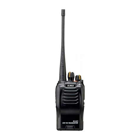
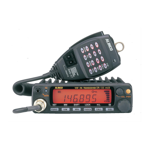
Alinco DJ-G5 User manual

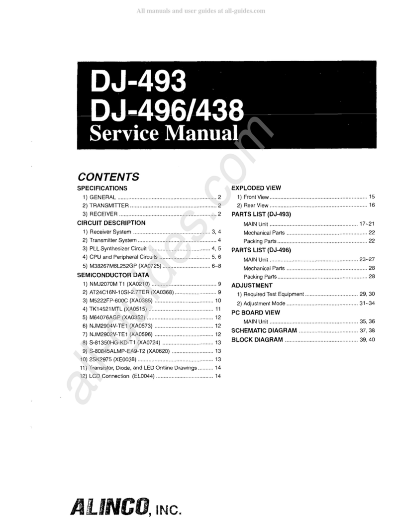
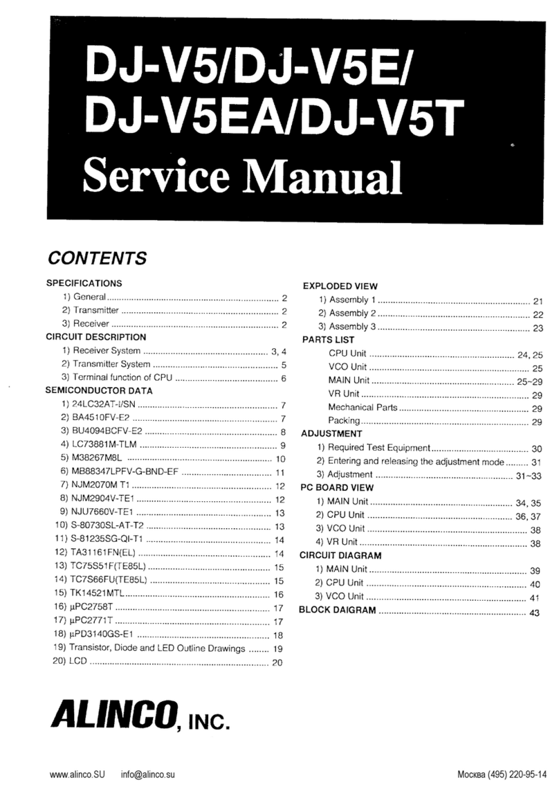
DJ-G5 Service Manual
CONTENTS
+ SPECIFICATI
O
NS 2+ PARTS LIST
RF Unit 37~40
IF Unit 41~44
+ CIRCUIT DESCRIPTI
O
NCPU Unit 44~46
1) Receiver System 3~5 SVV UniL 46
2) Transmitter System 5 UVCO Unit 46
3) PLL Synthesizer Circuit 6 VVCO Unit 47
4) CPU and Peripheral Circuit 6~7 CHARGE Unit 47
5) Terminal function of CPU 10~12 PTT Unit 47
6) Terminal function of 4094 13 Mechanical Parts 48
7) Frequency Table 13
+ SEMIC
O
NDUCT
O
R DATA + ADJUSTMENT
l) AK2341 14 1) Required Test Equipment 49
2) BU4094BF 15 2) Adjustment for DJ-G5T/E 50
3) HD6433877 16 3) Adjustment Points 51
4) LC75366M 17
5) LC73881 M 18
6) M64076GP 19 + PC B
O
ARD VIEW
7) MC3372VM 20 1) RF Unit Side A 52
8) NJM21 00V 20 2) RF Unit Side B 53
9) NJM2070M 21 3) IF Unit Side A 54
10) RH5RH501A 22 4) 1F Unit Side B 55
11) RH5RH651A 22 5) CPU Unit Side A 56
12) S-80730SL-AT 23 6) CPU Unit Side B 57
13) S-AV28 24 7) UVCO Unit 58
14) S-AU57 24 8) VVCO Unit 58
15) S-81237SG-QE 25 9) PTT Unit Side A 58
16) TA75S01F 25 10) PTT Unit Side B 58
17) TA75W01FU 26 11) CHARGE Unit 58
18) TC4W53F 26 12) SW Unit Side A 58
19) TK10930VTL 27
20) uPD1 6430AGF-3B9 28
21) 24LC16B 29 + V
O
LTAGE TABLE
22) Transistor, Diode and LED Outline Dr
a
30 1) Diode 59~60
23) LCD Unit 31~32 2) IC 60~63
3) Transistor 63~64
+ EXPL
O
DED VIEW
1) Charge Unit 33 + BL
O
CK DIAGRAM 66~67
2) RF Unit 34
3) IF Unit/CPU Unit 35
4) Front/Rear View 36 + SCHEMATIC DIAGRAM
1) RF Unit 68~69
2) IF Unit 70~71
3) CPU Unit 72~73
4) UVCO Unit 74
5) VVCO Unit 75
6) CHARGE Unit 76
7) PTT Unit 76
ALINCO INCORPORATED
TWIN 21 M.I.D. TOWER BUILDING 23F, 1-61, 2-CHOME,
SHIROMI CHUO-KU , OSAKA, 540-8580 JAPAN
Tel (81)6-6946-8150 fax (81)6-6946-8175
e-mail: [email protected]

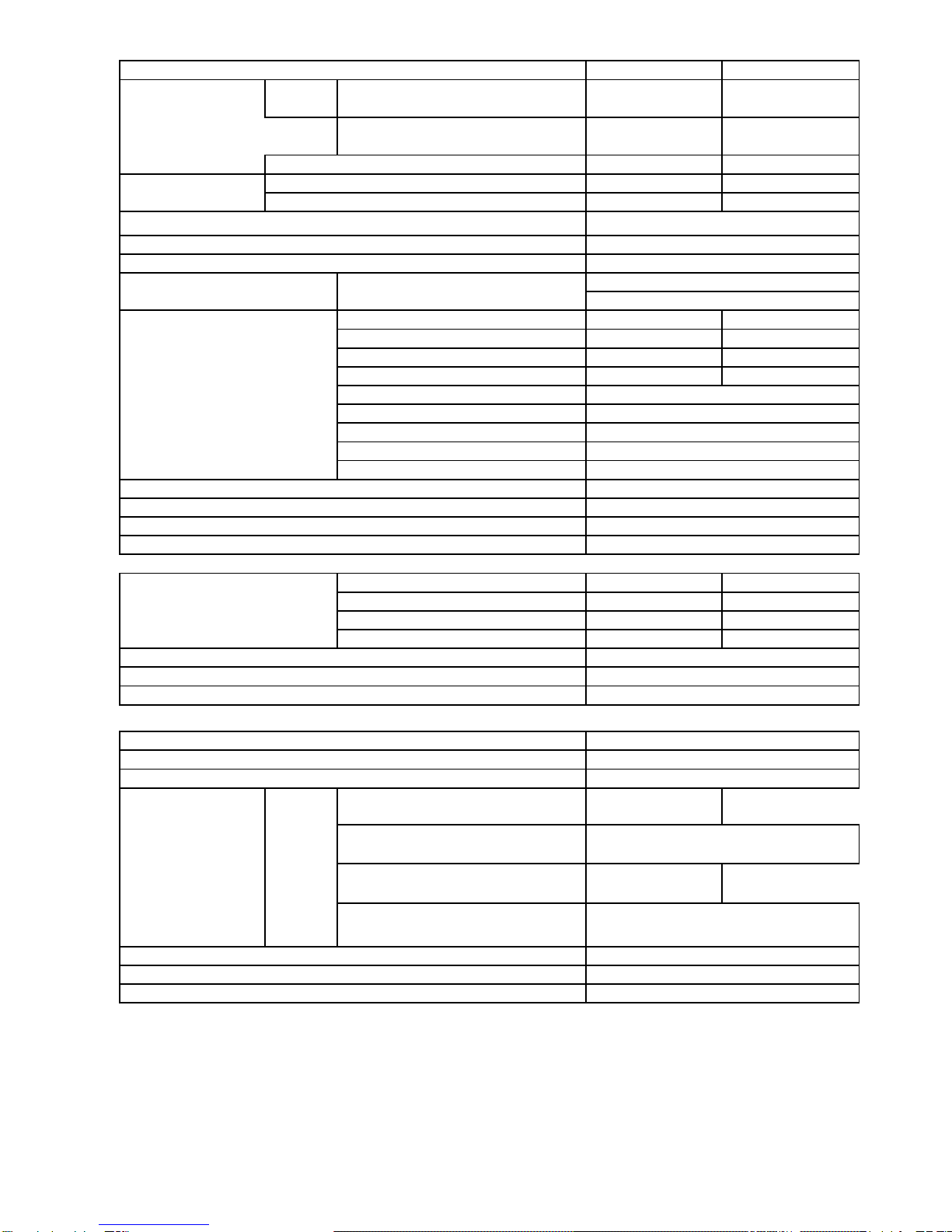
General VHF UHF
DJ-G5T L-band 108.000~173.995
(AM FM) 420.000~479.995
(FM)
Receiver range(MHz) R-band 1 30.000~l 73.995
(FM)
DJ-G5E 144.000~145.995 430.000~439.995
Transmitter range(
M
DJ-G5T 144.000~147.995 438.000~449.995
DJ-G5E 144.000~145.995 430.000~439.995
Modulation
Antenna impedance
Operating temperature range
Supply voltage (rated voltage) External (V)
Ni-Cd(V)
Tx Hi: 13.8VDC(external) approx. 1.4A approx. 1.5A
Tx Hi: 9.6VDC(Ni-Cd) approx. 1.4A approx. 1.5A
Tx Hi: 7.2VDC(Ni-Cd) approx. 1.4A approx. 1.5A
Tx Hi: 4.8VDC(Ni-Cd) approx. 1.0A approx. 1.2A
Current TxMid: 4.8VDC(Ni-Cd)
(regulated supply voltage) TxLo: 4.8VDC(Ni-Cd)
Rxsquelched(twinband)
Rxsquelched(monoband)
Rx Battery-Save On (800/200 twin band)
Ground
Microphone impedance
Dimensions without projection (with projections)
Weight (Ant. belt-clip, strap, and Ni-Cd EBP-33N inclusive)
Transmitter Hi: 13.8VDC(external) approx. 5W
Power output Hi: 9.6VDC(Ni-Cd) approx. 4.5W
(regulated supply voltage) Hi: 7.2VDC(Ni-Cd) approx. 3.5w approx. 3W
Hi: 4.8VDC(Ni-Cd) approx. l.5W approx. 1 W
Modulation
Maximum deviation
Spurious emission
Receiver
System Double-conversion superheterodyne
First l.F. 38.9MHz 45.1 MHz
Second l.F.
Sensitivity L-band:
1
44.
000
~
1
47.
99
5MHz
R-band: 438.000~449.995MHz better than -16dB
u
better than -15dBu
DJ-G5T L-band: 438.000~449.995MHz
R-band: 144.000~147.995MHz
L-band: 144.000~145.995MHz
R-band: 430.000~439.995MHz better than -16dB
u
better than -15dBu
DJ-G5E L-band: 430.000~439.995MHz
R-band: 144.000~145.995MHz
Squelch sensitivity
Selectivity (-6dB/-60dB)
A.F.output(@10% distortion)
455kHz
Variable reactance
+/-5kHz
notmorethan-60dB
approx. 0.8A
approx. 0.5A
approx. 85mA
approx. 50mA
approx. 350g
F2E.,F3E(FM)
50 ohm
-10 ~ +60*C
4.5~16.0(13.8)
4.5~16.0(4.8)
approx. 25mA
Negative ground
2k ohm
W57(63) x H138(155) x D27.5(31.5)
100mW(8ohm load)
better than-12dBu
better than -12dBu
better than-20dBu (0.1uV)
more than 12kHz / less than 30kHz

CIRCUIT DESCRIPTTON
1) Receiver System
The receiver system is the double-conversion superheterodyne. ln L band the first
IF is 38.9MHz and second IF is 455kHz, and in R band the first IF is 45.1MHz and
second IF is 455kHz.
1 Front End
1-1 108.00MHz~ 173.995MHz (144M Band Main)
The receiving signal is passed through the low-pass filter (L90, L91 , L92, C220,
C229, C230, C231, C235), and amplified in RF amplifier (Q77), then led to the
resonant circuit (L85, L86, varicap D68, D69). The signal is amplified in RF
amplifier Q75, and passed through the resonant circuit (L81 , L82 varicap D66 and
D67), then converted into the frequency of 38.9MHz in the mixer Q79.
Two resonant circuits consisting of L85, L86, varicap D68, D69, L81 , L82, varicap
D66, D67, are controlled by the trucking voltage to obtain the best condition to the
receiving frequency.
The local signal from VVCO OUT is passed through the buffer Q79, and fed to the
base of the mixer Q76. The sum of the displayed frequency and IF frequency is
employed.
1-2 420.00MHz~51 1.995MHz: (430M Band Sub)
The receiving signal is passed through the band-pass filter (C59, C60, C61 , C66,
C67, C68, L57, L58, L53, L54), RF amplifier (Q62, Q72), band switch (D63), and
high-pass filter (C175, C176, C186, C187, L77, L78), and converted into the
frequency of 38.9MHz in mixer (Q74).
The local signal is passed through the buffer (Q70), and the difference frequency
between IF frequency and the displayed frequency is fed to the base of the mixer
(Q74).
1-3 130.00MHz~173.995MHz (144M Band Sub)
The receiving signal is passed through the low-pass filter (L90, L91 , L92, C220,
C229, C230, C231 and C235), and RF amplifier (Q68), low-pass fitter (C145,
C146, C153 and C154), then converted into the frequency of 45.1MHz in the mixer
(Q67).
The local signal is passed through the buffer (Q69), then the sum of displayed
frequency and IF frequency is fed to the base of the mixer (Q67).
1-4 420.00MHz~51 1.995MHz (433M Band Main)
The receiving signal is passed through the band-pass filter (C59, C60, C61 , C66,
C67, C68, L57, L58, L53, L54), RF amplifier (Q62, Q72) and the band-pass filter
(FL51), and amplified in RF amplifier (Q63), then converted into the frequency of
45.1MHz.
The band-pass filter (FL51) is the helical filter to obtain the band width characteris-
tics.
The local signal from UVCO OUT is passed through the diode switch (D58), buffer
(Q64), then the difference frequency between the displayed and IF is fed to the
base ofthe mixer (Q61).
2 IF
2-1 L Band The sum/difference between the receiving signal and local signal is made in each
mixer. The crystal filter (XF53) selects the difference of 38.9MHz and
eliminates unwanted signal, then it is amplified in the first IF amplifier (Q78).
2-2 R Band The sum/difference between the receiving signal and local signal is made in each
mixer. The crystal filter (XF51) selects the difference of 45.l MHz and
eliminates unwanted signal, then it is amplified in the first IF amplifier (Q60).3
3 Demodulation
3-1 L Band After amplified in the first IF amplifier (Q78), the signal is fed to the demodulation
IC (IC302) Pin24. The first IF signal outputted to Pin24 (38.9MHz) is mixed in the
mixer of IC302 with the local signal of 38.455MHz which is oscillated in the
oscillation circuit of IC302 and the crystal oscillator (X303), then converted into the
second IF signal of 455kHz. The second IF is supplied from the IC302 Pin3. After
eliminating unwanted signal by the ceramic filter (FL302), the signal is applied to
Pin5 and Pin7.
As for the FM demodulation, the second IF signal applied to Pin7 is demodulated
in limiter amplifier and quadrature detection circuit of IC302 when IC302 Pinl4 is
open, and it is outputted from Pinl2 as the audio signal.
As for the AM demodulation, the second IF signal applied to Pin5 is demodulated
in AM amplifier and AM detection circuits of IC302 when the voltage of IC302
Pin14 is low, and it is outputted from Pinl3 as the audio signal.
3-2 R Band After amplified in the first IF amplifier (Q60), the signal is applied to the demodula-
tion lC301, Pinl6. It is mixed in the mixer of IC301 with the local signal of
45.555MHz which is oscillated in the oscillation circuit and the crystal oscillator
(X301) of IC301, then converted into the second IF signal of 455kHz. The second
IF is outputted from IC301 Pin3, and applied to Pin5 and Pin7 after eliminating
unwanted signal by the ceramic filter (FL30l).
4 Audio Circuit
4-1 FM (L bandThe audio signal supplied from IC302 is pre-emphasized white transmitting. So
the audio frequency should be compensated in the de-emphasis circuit (R366,
C363), then the signal is passed through FM/AM selection switch (IC303). The
frequency of 300Hz or below is cut in the audio high-pass fitter circuit (Q313), and
it is applied to the electronic volume (IC304) Pin1. The signal is passed through
the buffer (IC306), and adjusted the volume, then led to the audio power amplifier
(IC307) to drive the speaker.
4-2 AM (L ban
d
When AM mode is selected, the switching transistor (Q312) is turned ON, and
IC302 Pin14 becomes low, then AM demodulation circuit of IC302 is activated.
The audio signal provided from IC302 Pin14 is passed through the de-emphasis
circuit (R362, C360), and FM/AM selection switch (IC303), then led to audio high-
pass filter circuit (Q313), electronic volume (IC304), buffer (IC306) and the audio
power amplifier (IC307) to drive the speaker.
Note:
The FM detection circuit in IC301 (TK10930) is operating even while AM receiving.
(The squelch circuit is activated by FM detection output.) So the FM audio is not
outputted by FM/AM selection switch (IC303).
4-3 FM (R band)
The audio signal supplied by IC301 Pin9 is compensated the audio frequency
characteristics in de-emphasis circuit (R330, C327), and the signal is passed
through the audio high-pass filter (Q306), then applied to the electronic volume
(IC304) Pin20. It is passed through the buffer (IC305), and led to the audio power
amplifier (IC307) to drive the speaker.
5 Squelch Circuit
5-1 L Band A part of the audio signal of IC302 Pin12 is selected and amplified by the noise
amplifiers in R351 , R352, R350, R353, C351, C352, C353, and IC302. Then it is
supplied from IC302 Pin20 to be amplified again in the noise amplifier (Q309). The
amplified noise factor is rectified in D302, adjusted the level in VR303, and applied
to CPU (IC508) Pin96, then converted to the digital signal. 4

5-2 R Band A part of the audio signal of IC301 Ping is selected and amplified by the noise
amplifiers in R316, R317, R318, R319, C318, C319, C320, and IC301. Then it is
supplied from IC301 Pin11 to be amplified again in the noise amplifier (Q303). The
amplified noise factor is rectified in D301 , adjusted the level in VR30l , and applied
to CPU (IC508) Pin97, then converted to the dligital signal.
6 Attenuator Circuit
6-1 VHF Band When the ATT key is pressed, "L" is applied from shift resistor (IC52) Pin14, and
D71 is turned ON, then the Attenuator circuit (Q56, R151, C194, R160) is acti-
vated.
The receiving signal passed through the low-pass filter is attenuated approximately
15dB by the attenuator to decrease the interference of the adjacent channel, etc.
6-2 UHF Band When the ATT key is pressed, "L" is applied from shift resistor (IC52) Pin13, and
D55 is turned ON, then the Attenuator circuit (Q56, R73, C90, R80) is activated.
The receiving signal passed through the low-pass filter is attenuated approximately
15dB by the attenuator to decrease the interference of the adjacent channel, etc.
2) Transmitter System
1 Demodulation Circuit
The voice is converted into the electric signal by the internal or external micro-
phone, then it is applied to the mic amplifier (IC310). This IC310 has two opera-
tional amplifiers. The pre-emphasis and IDC consist of Pin1, 2 and 3, and the
splutter filter consists of Pin5, 6 and 7.
The output from the microphone amplifier is passed through variable resistors
VR305 and VR306 for maximum deviation adjustment to cathode of varicap diode
of the VCO, controlling the VCO frequency and so producing a frequency-modula-
tion.
2 Power Amplifier
2-1 The transmitting signal oscillated in VVCO is amplified in pre-drive amplifier (Q81)
and drive amplifier (Q80), then fed to the power module (IC54). The transmitting
signal amplified in IC54 is supplied to the antenna after attenuated the harmonics
enough in the antenna switch (D72) and the Low-pass filter (L90, L91 , L92, C220,
C229, C230,C231 , C235).
2-2 The transmitting signal oscillated in UVCO is amplified in pre-drive amplifier (Q54)
and drive amplifier (Q53), then fed to the power module (IC51). The transmitting
signal amplified in IC51 is supplied to the antenna after attenuated the harmonies
enough in the antenna switch (D52), and the bandi)ass filter (L57, L58, L53, L54,
C59, C60, C61, C66, C67, C68).
3 APC Circuit
3-1 VHF Band A part of transmitting voltage from low-pass filter is detected by D74, and con-
verted into the DC voltage. The converted detection voltage is differential ampli-
fied, and the output voltage controls the bias voltage of power module (IC54) Pin2
to fix the transmitting power.
3-2 UHF Band A part of transmitting voltage from low-passS filter is detected by D56, and con-
verted into the DC voltage. The converted detection voltage is differential ampli-
fied, and the output power controls the bias voltage of power module (IC51) Pin2
to fix the transmitting power. 5

3) PLL Synthesizer Circuit
1 PLL The data is sent to the PLL IC (IC53) Pin2 and the clock is sent to Pin3 from CPU
(IC508), then the ratio of the division is decided each in L band and R band.
Each VCO oscillating signal is amplified in the buffer (Q73: L band, Q66: R band),
and the signal in L band is applied to Pin15, then the signal in R band is applied to
Pin6. The programmable divider of IC53 is determined by frequency data, and it
divides (1/N) input signal of IC53. Resulting signal will be 5kHz or 6.25kHz.
2 Reference frequency division
The reference frequency of 5kHz or 6.25kHz according to the channel step is
produced by dividing the reference oscillation 12.8MHz (X51) by 2560 or 2048, the
data from CPU (IC508). The channel steps of 5kHz, 10kHz, 15kHz, 20kHz,
25kHz, 30kHz and 50kHz use the reference frequency of 5kHz, and the channel
step of l2.5kHz uses the reference frequency of 6.25kHz.
3 Phase comparator
The reference frequency of IC53 is 5kHz or 6.25kHz.
The VCO output frequency divided by N is compared with 5kHz or 6.25kHz in the
phase comparator.
4 PLL Loop Filter Circuit
If the phase error should occur in PLL, the charge pump of IC53 Pin13 (L band)
and Pin8 (R band) outputs the pulse. The signal is converted into the DC voltage
in PLL loop filter, then inputted to the varicap of each VCO unit.
5 VVCO Circuit (VHF Band)
Q705 is turned ON, and the desired frequency is oscillated in the Colpitts osclllator
consisting of Q701. The frequency control voltage is apprled to the varicap (D702,
D703), and the osciflating frequency is changed, then amplified in VCO buffer
(Q703), and outputted from the VCO unit.
6 VVCO Circuit (UHF Band)
Q704 is turned ON, and the desired frequency is oscillated in the Colpitts oscillator
consisting of Q702. The frequency control voltage is applied to the varicap (D704,
D705), and the oscillating frequency is changed, then amplified in VCO buffer
(Q703), and outputted from the VCO unit.
7 UVCO Circuit (UHF Band)
Q605 is turned ON, and the desired frequency is oscillated in the Colpitts oscillator
consisting of Q601. The frequency control voltage is applied to the varicap (D602,
D603), and the oscillating frequency is changed, then amplified in VCO buffer
(Q603), and outputted from the VCO unit.
8 UVCO Circuit (VHF Band)
Q604 is turned ON, and the desired frequency is oscillated in the Colpitts oscillator
consisting of Q602. The frequency control voltage is applied to the varicap (D604,
D605), and the oscillating frequency is changed, then amplified in VCO buffer
(Q603), and outputted from the VCO unit.
4) CPU and Peripheral Circuit
1 LCD Display Circuit
The strobe, serial data, and clock are sent to the LCD driver (IC503) Pin 75~77
from CPU (IC508), and the LCD is activated with 1/4 duty and l/3 bias. The frame
frequency is 137Hz. 6

2 Display Lamp Circuit
The regulated power supply circuit consisting of Q505, Q507, R508, R509 supplies
H from CPU (IC508) when LAMP key is pressed. Then it is applied to the base
of Q507, and the voltage of 3.5V is outputted from the collector of Q505. lt is fed
to each LED (D503~D506, D509,D511 ,D513,D514).
3 Reset and Backup Circuit
When the voltage of approximately 3.0V or more is supplied from the external (DC
jack, battery), the reset signal of "H" level is outputted from Reset IC (IC506), and
it is fed to CPU (IC508) Ping, then the CPU is reset. Until the clock (X502) of CPU
is stabilized, the reset signal is fed to CPU after it is delayed in C522 and R58l.
When the voltage from external is decreased to approximately 3.3V or below, the
voltage of Pin18 in CPU is changed from "H" level to "L" level, then the CPU enters
into the backup mode.
4 S (signal) Meter Circuit
4-1 L Band The DC voltage of IC302 Pin16 is low when the signal is weak and high when the
signal is strong. This change of DC voltage is adjusted the level at the trim pot
(VR304), and led to CPU (IC508) Pin98, then displayed on the LCD as S meter
after A/D converting.
4-2 R Band The DC voltage of IC301 Pin13 is adjusted the level at the trim pot (VR302), and
led to CPU (IC508) Pin99, then displayed on the LCD as S meter after A/D
converting.
5 Full-duplex Circuit
When the DUP key is pressed, in the receiving side Q317 is turned ON and the
audio signal supplied to audio amplifier is decreased. ln transmitting side Q510 is
turned ON, and the modulation signaf is decreased to prevent the howling.
6 X-Band Repeater Circuit
ln X-band repeater mode, Q323 is turned OFF, the audio Signal which is opened
the squelch is passed through the audio high-pass filter (Q313: L band, Q306:R
band), and the signal is applied to the other modulation circuit. Then the radio
enters into the transmitting mode.
7 DTMF
7-1 Encoder The DTMF encoder is built in the CPU (IC508). The DTMF signal output from
Pin91 is adjusted its level at VR308, and amplified by the mic amplifier (IC310),
then fed to the varicap for modulation of each VCO.
Simultaneously the monitor sound is passed through AF circuit, and it is supplied
from the speaker.
7-2 Decoder A part of the audio signal which is demodulated in IC301 , IC302 is fed to the DTMF
switch (IC501), then only the selected band audio signal is fed to DTMF IC (IC502)
Pin1. The supplied signal is judged whether valid or not by the signal judgement
circuit in IC502, and converted into 4-bit code, then supplied to IC508 Pin85.
8 Tone Squelch
8-1 Encoder The tone signal supplied from Tone IC (IC504) Pin21 (67.OHz~254.lHz) is ad-
justed the level at VR307, and amplified n the tone amplifier (Q322), then applied
to the varicap for modulation of each VCO.
8-2 Decoder A part of the audio signal which is demodulated in IC301, IC302 is fed to the tone
switch (IC504), then only the selected band audio signal is fed to tone IC (IC504)
Pin1.
When the signal is accord with the programmed tone frequency, "LO" is outputted
from IC504 Pin14, and it is fed to CPU (IC508) Pin74, then the squelch is opened.
7

5) Terminal function of CPU
No. Name Pin Name I/O Description H L HiZ
1 ANO +BD I Power supply voltage detection Analog lN
2 AVSS GND / Analogground
3 TEST GND / Connect to ground
4 X2 OPEN Open when not used
5 X1 VDD / Power supply
6 VSS GND / Ground
7 OSC1 OSC1 I Internal oscillator input
8 OSC2 OSC2 O Internal osciIIator output
9 RES REST I CPU reset At work
10 NMl VDD /
11 P20 CLK O Clock input Pulse Normal
12 P21 DATA O Data input Pulse Normal
13 P22 STB1 O RF4094 strobe Pulse Normal
14 P23 STB2 O lF4094 strobe Pulse Normal
15 P24 STB3 O Electronic volume strobe Pulse Normal
16 P25 OPEN /
17 P26 +BDSW O +BD input ON/OFF ON OFF
18 lRQO BU I Backup signal input Normal Backup
19 P17 RE1 I Rotary encoder up input OFF ON
20 P16 RE2 I Rotary encoder down input OFF ON
21 P15 PSW I Power switch input OFF ON
22 P14 OPEN
23 P13 OPEN
24 TMOFH BEEP O Beep sound output Pulse Pulse Normal
25 TMOFL 1750 O Tone burst output Pulse Pulse Normal
26 P10 XBR O Cross band repeater ON/OFF Normal Repeater
27 VSS GND / Ground
28 V3 OPEN
29 V2 OPEN
30 V1 OPEN
31 VCC VDD / Power supply terminal
32 PA3 LBSY I LCD driver data input ON/OFF Permitted Inhibited
33 PA2 LCLK O LCD driver clock Normal Pulse
34 PA1 LDATA O LCD driver serial data Normal Pulse
35 PA0 LSTB O LCD driver strobe Inhibited Permitted
36 P50 PT5/PTT I PTT input ON OFF
37 P51 MONt I Monitor key input OFF ON
38 P52 TBST I TX(toneburst)input OFF ON
39 P53 FUNC I Function key input OFF ON
40 P54 BP3 I Band plan (TX/RX expansion) Expanded Normal
41 P55 UHF I UHF key input OFF ON
42 P56 VOLU I VOL up key input OFF ON
43 P57 SQLD I SQL down key input OFF ON
44 P60 SQLU I SQL up key input OFF ON
45 P6l SRCH I Search key input OFF ON
46 P62 VHF I VHF key input OFF ON
47 P63 VOLD I VOL down key input OFF ON
48 P64 KIN1 I Key matrix input1 OFF ON
49 P65 KIN2 I Key matrix input2 OFF ON
50 P66 KIN3 I Key matrix input3 OFF ON 10

No. Name Pin Name IIo Description H L HiZ
51 P67 KIN4 I Key matrix input4 OFF ON
52 P70 KOT1 O Key matrix output1 OFF ON
53 P71 KOT2 O Key matrix output2 OFF ON
54 P72 KOT3 O Key matrix output3 OFF ON
55 P73 KOT4 O Key matrix output4 OFF ON
56 P74 PRST O PLL reset pulse input judgement Normal Pulse
57 P75 SDA I/O EEPROM data PL SE Normal
58 P76 SCL O EEPROM clock PL SE Normal
59 P77 50SW O 5V ON/OFF ON OFF
60 P80 OPEN /
61 P81 TFD O Full duplex ON/OFF when transmittin Full duplex Normal
62 P82 UTBST O Right side TX lamp ON/OFF ON OFF
63 P83 VTBST O Left side TX lamp ON/OFF ON OFF
64 P84 VTXCV O VHF TX circuit for power supply ON OFF
65 P85 UTXCV O UHF TX circuit for power supply ON OFF
66 P86 VBSY O VHF RX busy lamp ON/OFF ON OFF
67 P87 UBSY O UHF RX busy lamp ON/OFF ON OFF
68 P90 LAMPC O LAMP ON/OFF ON OFF
69 P91 PCNT O Vcc ON/OFF ON OFF
70 P92 MUTE O Microphone mute Muted Normal
71 P93 RFD O Full duplex ON/OFF when receiving Full duplex Normal
72 P94 DSW O DTMF band selection VHF UHF
73 P95 TSW O Tone band selection VHF UHF
74 P96 TSQD I Tone detection signal input None Tone
75 P97 TSTB O Tone IC strobe Pulse Normal
76 VCC VDD / Power supply
77 PD0 AM O AM circuit ON/OFF AM FM
78 PD1 AFPC O Audio amplifier power supply ON/OF
F
ON OFF
79 PD2 VAFS O VHF AF mute Muted ON
80 PD3 UAFS O UHF AF mute Muted ON
81 PD4 OPEN
82 PD5 IFPC O IF power supply ON/OFF ON OFF
83 PD6 VRXC O VHF IF circuit power supply OFF ON
84 PD7 URXC O UHF IF circuit power supply OFF ON
85 PE0 DSD I DTMF 4-bit data Normal Pulse
86 PE1 ACK O DTMF clock Pulse Normal
87 PE2 DSTD I DTMF detection signal Signal None
88 PE3 DPD O DTMF operation ON/OFF isstopped Operation
89 AVCC AVCC / A/D converter power supply
90 TONEM TRAC O VHF trucking voltage output
91 TONED DTON O DTMF signal output Normal
92 VTref VDD / Power supply for DTMF reference level
93 AVref AVCC / Power suppTy for A/D reference level
94 AN7 BP2 I Band plan2
95 AN6 BP1 I Band plan1 (destination)
96 AN5 VSD I VHF SD signal input No signal Analog in
97 AN4 USD I UHF SD signal input No slgnal Analog in
98 AN3 VSMT I VHF S meter signal input Analog in
99 AN2 USMT I UHF S meter signal input Analog in
100 AN1 MRC I Microphone remote control input Analog in 11

6) Terminal function of 4094
4094 p
o
Port Name Function Logic Description
VHF
145
MHz
VHF
433
MHz
UHF
433
MHz
UHF
145
MHz
BS
OFF
TIME
Q11 UHl UHF high power control Active Low Low power H H H H H
Q12 UMlD UHF middle power control Active Low UHF middle=H H H H H H
Q13 VHl VHF high power control Active Low Low power H H H H H
Q14 VMID VHF middle power control Active Low VHF middle=H H H H H H
Q15 VATTC VHF RX attenuater control Active Low ATT ON H/L H/L H/L H/L H
Q16 UATTC UHF RX attenuater control Active Low ATT ON H/L H/L H/L H/L H
Q17 VCO4SW UHF VCO switch Active Low H/L H/L L H H
Q18 VCO1SW VHF VCO switch Active Low L H H/L H/L H
Q21
Q22 USUBC UHF 145MHz power control Active Low H/L H/L H L H
Q23 UMAINC UHF 435MHz power control Active Low H/L H/L L H H
Q24
Q25 VSUBC VHF 435MHz power control Active Low H L H/L H/L H
Q26 VMAlNC VHF 145MHz power control Active Low L H H/L H/L H
Q27 UPLLC UHF VCO power control Active Low H/L H/L L L H
Q28 VPLLC VHF VCO power control Active Low L L H/L H/L H
7) Frequency Table
Band IF Frequency Display frequency UP/LOW Oscillation frequency Mode
VHF 38.9MHz 108.000~173.995MHz UP 146.900~212.895MHz FM/AM
420.000~511.995MHz Low 381.100~473.095MHz FM/AM
UHF 45.lMHz 130.000~173.995MHz UP 175.100~219.095MHz FM
420.000~511.995MHz Low 374.900~466.895MHz FM
13


(XA0505)


Other manuals for DJ-G5
1
Other Alinco Transceiver manuals

Alinco
Alinco DR-M06T Guide

Alinco
Alinco DJ-A446 Owner's manual

Alinco
Alinco DJ-100 User manual

Alinco
Alinco DJ-FX446 User manual

Alinco
Alinco DR-570T User manual

Alinco
Alinco DJ-580T User manual

Alinco
Alinco DJ-G29T User manual

Alinco
Alinco DX-SR9 User manual

Alinco
Alinco DJ-S46 User manual

Alinco
Alinco DJ-G7 User manual

Alinco
Alinco DR-150T User manual

Alinco
Alinco DJ-G1T User manual

Alinco
Alinco DJ-CRX1 User manual

Alinco
Alinco DR-MX15 User manual

Alinco
Alinco DR-735T(2) User manual

Alinco
Alinco DJ-A10 User manual

Alinco
Alinco DR-MD520T User manual

Alinco
Alinco DJ-G29T User manual

Alinco
Alinco DR-235T User manual

Alinco
Alinco DR-140T User manual