Alinco DJ-100 User manual

* Specifications
* Circuit Description
* Parts list
* Schematic Diagram
* Block Diagram
* PC Board View
* Mechanical Parts
ALINCO, INC.
DJ-100
Service Manual
Service ManualService Manual
Service Manual

DJ-100
SPECIFICATIONS
General
Frequency Range RX: 136~174MHz
TX: 136~174MHz
Number of channels Max.200
Channel Spacing 12.5kHz /20kHz/25kHz
PLL Channel Stepping 5kHz, 6.25kHz
Operating Voltage 7.4 V DC ±20%
Battery Life More than12 hours at 5 watts (5-5-90 duty cycle with 1500mAh Li battery)
Operating Temperature range –20°C to +55°C
Dimensions and Weight
With EBP-87 (1500mAh battery) 59W x 98H x 35D mm 220g
Frequency Stability ±2.5ppm (–20°C to +55°C)
Channel Frequency Spread 38MHz
Receiver (Measurements made per TIA/EIA-603)
RF Input Impedance 50Ω
Sensitivity
EIA 12dB SINAD Wide : 0.25μVNarrow : 0.35μV
Selectivity . Wide : 70dB Narrow : 60dB
Intermodulation distortion Wide : 65dB Narrow : 60dB
Spurious response 70dB
Audio
Power Output
1000mW at16Ωless than10% distortion
First IF 38.85MHz
Second IF 450KHz
Transmitter (Measurements made per TIA/EIA-603)
RF Power Output
HI : 5W Mid : 2W LO : 0.5W
RF Output Impedance 50Ω
Spurious and Harmonics 60dB
Modulation Wide : 16K0F3E Narrow : 11K0F3E
FM Noise Wide : 45dB Narrow : 40dB
Audio Distortion W/N : Less than 5%(1000Hz, 60%modulation)
2

DJ-100
3
ANT SW RF
AMP
MCF
38.850MHz
IF SYSTEM
450KHz
CF
ANT
AF
AMP SP
FINAL
PRE
DRIVE
PLL
VCO MIC
MIC
AMP
MIX
TCXO 19.200MHz
Tripler
38.40MHz
X3
RX/TX:136 ~ 17 4MHz
DRIVE
ANT SW
IF,MIX,DET
LV
ANT
AF AMP
SP
1st Loca l OSC
AF PA AMP
U205
U502
IF AMP
Q509
MCF
XF500,XF501
MI XER
Q506
BPF
RF AMP
Q506
BPF
D517
2nd Loca l OSC
D503,D504
VFO
.
Q510
Tri pl e r X3 TCXO 19.200MHz
X500
U206
MPU
U203B
38.400MHz
VCO PLL
(PLL)
Tun ing vol tage
AQUA
U200
CF500
CIRCUIT DESCRIPTION
1. Overview
This transceiver is a VHF portable transceiver designed
to operate in the frequency range of 136 to 174MHz.
The unit consists of receiver, transmitter, phase-locked
loop (PLL) frequency synthesizer, base band parts, power
supply, and control circuits.
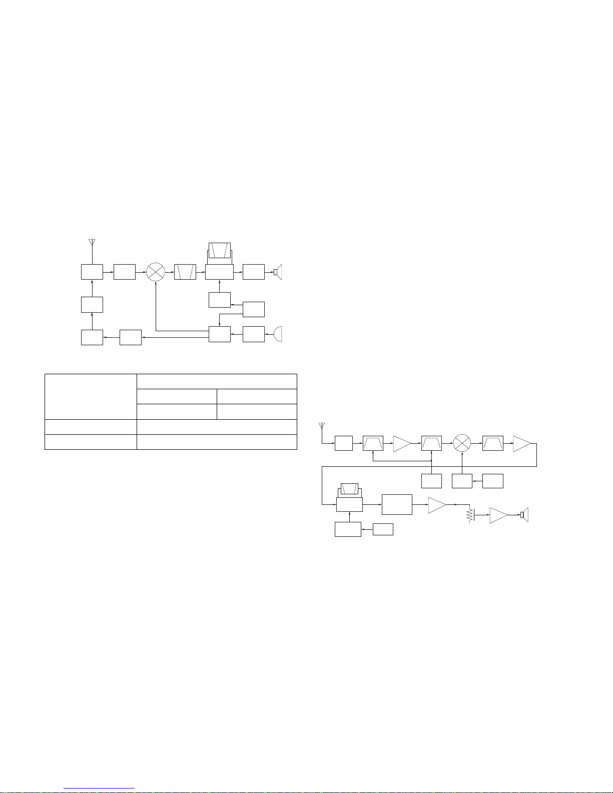
2. Frequency Configuration
The frequency configuration is shown in Figure 1 and
Table 1.
Fig. 1 Frequency configuration
Table 1 Basic configuration
3. Receiver
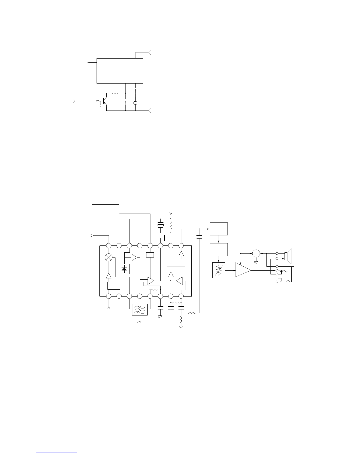
3-1-1. Front-end RF Amplifier
The received signal from the antenna passes through a
low-pass filter and then through a transmission/reception
switching circuit (antenna switch) and enters the tuned
filter (L510).
The signal passing through the band-pass filter (L510) is
amplified by with an RF amplifier (Q505), passes through a
band-pass filter (L512, L542) and enters the first mixer
(Q506).
These band-pass filters are tuned to a desired frequency
by varicaps (D509, D510, D511, D512).(See Fig.2)
A tuning voltage corresponding to the desired signal is
applied to each varicap through the VFO terminal (pin 60)
of the MPU (U206) to tune to the receive frequency.
3-1-2. First Mixer
The received signal passing through the band-pass filter
(L512, L542) is mixed with the first local signal generated
by the VCO by the first mixer (Q506) to produce a first IF
signal (38.85MHz) (Upper heterodyne).
The first IF signal passes through a MCF (Monolithic
crystal filter: XF500 and XF501) to remove unwanted
components.
The first IF signal passing through the MCF (XF500 and
XF501) is amplified by an IF amplifier (Q509) and the
resulting signal enters the FM IC (U502).(See Fig.2)
3-1-3. IF Amplifier Circuit
The first IF signal (38.85MHz) amplified by the IF
amplifier (Q509) and the second IF signal (45.9MHz)
generated by tripling the 19.200MHz reference oscillator
frequency of the TCXO (X500) by Q510, are mixed in the
FM IC to produce a second IF signal (450 kHz) (Lower
heterodyne).
The second IF signal passes through a ceramic filter
(CF500) to remove unwanted components.
The second IF signal passing through the ceramic filter
(CF500) passes through the IF amplifier in the FM IC again
and is detected to produced an audio signal.(See Fig.2)
Fig.2
3-1-4. Wide/Narrow Switching Circuit
Narrow and Wide settings can be made for each channel
by switching the demodulation level. The WIDE (low level)
and NARROW(high level) data is output from U206, pin 11.
When a WIDE (low level) data is received, Q507 turn on.
When a NARROW (high level) data is received, Q507
turn off.
Q507 turns on/off with the Wide/Narrow data and the U502
detector output level is switched to maintain a constant
output level during wide or narrow signals. (See Fig.3)
Reception method
Double super heterodyne
1st IF Frequency 38.85MHz (Upper)
2nd IF Frequency 450kHz (Lower)
Transmission method VCO direct oscillation amplification
Modulation Variable reactance phase modulation

DJ-100
4
QUAD
AFOUT
C580
T500
R551
R528
Q507
Q509
U502
FM SYSTEM
IFOUT
5R
P60 (U206)
L:Wide
H:Narrow
AF OUT
From MPU
SP MUTE
T500
2nd local OSC
CF500
450kHz
C654
R560
R591
(38.40MHz)
R549
Quadrature
detector
10 9
111213141516
87
654321
RSSI
Local
OSC
MIX
Rectifier
Nois e
comp
IF AMP
LPF
Inverter
AMP
AMP
Nois e
Buffer
C655
5R
P61
MPU
P00
P04 RSSI
SQ
U206
1st IF input
(38.85MHz)
AF OUT
SW
U200
SP
AF PA
LS200
U205
AQUA
U203B
J200
VOL
AMP
Q202,Q206
FM IC
U502
SW
CIRCUIT DESCRIPTION
Fig.3
3-1-5. Squelch and Mute Circuit
A noise component is obtained by passing FM
detection output (FM IC pin 9) through an operational
amplifier in the FM IC and band-pass filter consisting of
R549, R560, R591, C654, C655. The noise component is
rectified in the FM IC to produce a DC voltage, which is
output from the N-REC terminal (pin 14) of the FM IC as
squelch voltage.
The squelch voltage enters the SQ terminal (pin 50) of
the MPU (U206) and is compared with the reference
voltage preset in the MPU to control audio signal
ON/OFF.
To output sounds from the speaker, U206 sends a high
signal to the P61 line and turns U205 on through Q202
and Q206. (See Fig.4)
3-1-6. S Meter Circuit
The S meter voltage is output from the RSSI terminal
(pin 12) of the FM IC (U503) and input to the SM terminal
(pin 54) of the MPU. Then the voltage is converted from
analog to digital in the MPU to control the S meter display
on the LCD. (See Fig.4)
Fig.4
3-2. AF signal system
3-2-1. Audio amplifier circuit
The demodulated signal from U501 goes to Audio
processor through U200 (AF filtered, low-pass filtered,
high-pass filtered, De-Scrambler, Expander, and
de-emphasized).
The signal then goes through an AF amplifier U203B
(2/2), an AF volume control (W200), and is routed to an
audio power amplifier (U205), where it is amplified and
output to the internal speaker. (See Fig.5)
3-2-2. Receive Signalling
3-2-2-1 Low-speed data(CTCSS/DCS)
300 Hz and higher audio frequencies of the output signal
from IF IC are cut by IC (U502) within a low-pass filter.
U200 determines whether the CTCSS or DCS matches the

DJ-100
5
IF AMP DET
F M I F I C U 502
SP MUTE
U203A(1/2)
DTMF/2-TONE/5-TONE
HPF
52
U206
MPU
P02
AF
U203B(2/2)
AF AMP
SP
AF PA
LS200
U205
Q202,Q206
VOL
P30, P32, P33, P36, P37
U200
AQUA
P61
J200
56
50
P00 SQL
FI LTER
SW
COMPARATOR
PHASE CHARGE
PUMP
5KHz/6.25KHz
5KHz/6.25KHz
PLL IC U503
REF OSC
I/N
I/M
PLL DATA
LPF
D507,D518
VCO
Q517 BUFF AMP
Q516
19.200MHz
RF AMP
Q515
RF AMP
Q519
Q518
T/R SWP26
(U206 Pin 17)
MOD
MOD
Ripple
Filter
5C
Q512
From MPU
X500
5M
LD
U503
PLL IC
R597
C543
U206
P53
MPU
D501
CIRCUIT DESCRIPTION
preset value. If it matches, and controls the SP MUTE (P61)
the speaker on output sounds microprocessor (U206)
according to the squelch results.
3-2-2-2 High-speed data (DTMF/2 tone/5 tone)
The demodulated signal from the IF IC (U502) is
high-pass filter by U203A (1/2) to remove a low-speed data.
The MPU digitizes this signal, performs processing such as
DC restoration, and decodes the signal.(See Fig.5)
Fig.5
4. PLL frequency synthesizer
The PLL circuit generates the first local oscillator signal
for reception and the RF signal for transmission.
4-1.PLL circuit
A reference frequency of 5 kHz or 6.25 kHz is produced
by dividing the 19.200 MHz reference frequency of the
TCXO (X500) with PLL IC (U503). Comparison frequency
is produced by amplifying VCO output with an RF amplifier
(Q519) and dividing it with the PLL IC.
The PLL synthesizer with 5 kHz and 6.25 kHz step is
configured by comparing phases of the reference
frequency and comparison frequency.
The phase difference between reference frequency and
comparison frequency passes through a charge pump in
the PLL IC, then ripples are removed with a loop filter with
low-range passing characteristics to produce VCO control
voltage (lock voltage). (See Fig. 6)
4-2.VCO circuit
The VCO produces a desired frequency directly with a
Colpits oscillation circuit containing an oscillation transistor
(Q517) used for both transmission and reception.
The VCO control voltage is applied to varicap (D507,
D518) to produce a desired frequency.
The P26 terminal (pin 17) of the MPU (U206) goes "H"
during transmission, and the R/T control switch (Q518) is
turned OFF to change oscillation frequency. (See Fig. 6)
Fig.6
4-3. Unlock Detector circuit
If a pulse signal appears at the LD pin of U502, an
unlock condition occurs, and the DC voltage obtained from
C543, R597 and D501 causes the voltage applied to the
microprocessor to go low. When the microprocessor
detects this condition, the transmitter is disabled, ignoring
the push-to-talk switch input signal. (See Fig. 7)
Fig.7

DJ-100
6
ANT
LPF
U501B
ANT SW
FI NAL AMP
RF
DRIVE
AMP
RF
AMP
From
T/R SW
(D505)
+BATT
(2/2)
U501A
(1/2)
R590
R589
R588
APC
(U206)
VDDVG VG
Q514 Q511 Q502 D517
MIC AMP
U201
U202A(1/2)
MIC
U200
AQUA VCO
BUFF AMP
U206
MPU
TCXO
P06 58
P62
55MIC
MUTE
Q205
U202B(2/2)
BUFF AMP
CIRCUIT DESCRIPTION
5. Transmission signal system
5-1.Microphone Amplifier Circuit
The audio signal from the microphone passes through a
microphone amplifier (U201) and enters Audio processor
(U200). U200 is composed of Compressor,
pre-emphasis/IDC, Scrambler,limiter and Mux circuit.
The signal passes through the Audio processor (U200)
for the maximum deviation adjustment, and the buffer
amplifier U202B (2/2), and goes to the VCO modulation
input. (See Fig. 8)
5-2. Encode Signalling
5-2-1 Low-speed data(CTCSS/DCS)
CTCSS/DCS signal is generated by Audio processor
(U200). Output signal (U200 pin 35 and 36 (MOD) goes to
TCXO modulation and VCO modulation. (See Fig. 8)
5-2-2 High-speed data (DTMF/2 tone /5 tone)
High-speed data is output from pin 58 of the MPU. The
signal passes through a low-pass CR filter, and provides a
TX and SP out tone. The signal is mixed with the audio
signal and goes to the VCO. (See Fig. 8)
Fig.8
5-3. Drive and Final Amplifier Circuit
The signal from the T/R switch (D505 is on) is amplified
by the pre-drive (Q514) and drive amplifier (Q511) to
40mW. The output of the drive amplifier is amplified by the
RF power amplifier (Q502) to 5W (1W when the power is
low).
The RF power amplifier consists of two MOS FET
stages. The output of the RF power amplifier is then
passed through the harmonic filter (LPF) and antenna
switch (D517) and applied to the antenna terminal. (See
Fig. 9)
5-4. APC Circuit
The APC circuit always monitors the current flowing
through the RF power amplifier (Q502) and keeps a
constant current. The voltage drop at R588, R589 and
R590 is caused by the current flowing through the RF
power amplifier and this voltage is applied to the differential
amplifier U501(1/2). U501 (2/2) compares the output
voltage of U501 (1/2) with the reference voltage from U206.
The output of U501 (2/2) controls the VG of the RF power
amplifier, Drive amplifier and Pre-Drive amplifier to make
both voltages the same.
The change of power high/low is carried out by the
change of the reference voltage. (See Fig. 9)
Fig.9
6Control Circuit
The microprocessor (U206) operates at a clock of
19.200MHz.
The control circuit consists of a microprocessor (U206)
and its peripheral circuits. It controls the TX-RX unit. U206
mainly performs the following:
(1) Switching between transmission and reception by the
PTT signal input.
(2) Reading system, group, frequency, and program data
from the memory circuit.
(3) Sending frequency program data to the PLL.
(4) Controlling squelch on/off by the DC voltage from the
squelch circuit.
(5) Controlling the audio mute circuit by the decode data
input.
(6) Transmitting tone and encode data
(7) Controlling the LCD display circuit.

DJ-100
7
U207
EEPROM
U206
MPU
BATT1
R243
C215
U206
P03
MPU
R244
53
MPU
P14 , P1 5, P1 6, P 17
U2 06 LC D
U2
LCD
SEG1~SEG40
COM1~COM 16
driver
P85, P 86
Q1 ,Q2
SW LED
P81, P 82
D8 -D12
D6
SW
DS1
D5
D2 03
RX LED
D2 04
TX LED
P22
P23
Q504
VOL
BATT1
ON/OFF
3.3M
3.3V REG
U101
5C
U500
5V REG
P24
BATT
5M
5V REG
U210
RF power amp (Q502)
Q503
5R
5T
P20
P25
CIRCUIT DESCRIPTION
6-1. Memory Circuit
Memory circuit consists of the MPU (U206 and an
EEPROM (U207). An EEPROM has a capacity of 128k bits
that contains the transceiver control program for the MPU
and data such as transceiver channels and operating
features. (See Fig. 10)
Fig.10
6-2. Low battery warning
The battery voltage is monitored by the microprocessor
(U206). When the battery voltage falls below the voltage
set by the Low Battery Warning adjustment, the red LED
flashes to notify the operator that it is time to replace the
battery. If the battery voltage falls even more (approx.
6.0V), a beep sounds and transmission is stopped.
Low battery warning Battery condition
The red LED flashes
during transmission
The battery voltage is low but
the transceiver is still usable.
The red LED flashes
and a continuous beep
sounds while PTT
pressed.
The battery voltage is low and
the transceiver is not usable to
make calls.
Fig.11
7. Display Circuit
The MPU (U206) controls the display LCD and LEDs.
When power is on, the LCD driver will use the P81, P82
lines to control the LCD illumination (D5) and key backlight
LEDs (D208~D212 ).
The LCD driver (U2) and MPU (U206) communicate
through the P14, P15, P16, P17, P85, P86 lines.
When the reception is busy, P22 line becomes high
impedance, and the green LED (D203) lights, in transmit
mode, the P23 line becomes high impedance, and the red
Fig.12
8. Power Supply
There are four 5V power supplies for the microprocessor:
5M,5C,5R, and 5T. 5M for microprocessor is always output
while the power is on. 5M is always output, but turns off
when the power is turned off to prevent malfunction of the
microprocessor.
5C is a common 5V and is output when SAVE is not set to
OFF.
5R is 5V for reception and output during reception.
5T is 5V for transmission and output during transmission.
Battery +B is supplied via a ferrite chip from the battery
terminal connected to the TX-RX unit. After passing
through the power switch, power supply (BATT1) is applied
to the three AVRs. U210 supplies 5V (5M) to the control
circuit, and U101 supplies 3.3V (3.3M) to Audio processor
circuits, and U500 supplies 5V (5C) to common circuits.
U500 supplies to the TX circuit, the RX circuit and common
circuits of needless save mode. During transmission, P25
becomes Low and Q503 is turned ON to supply 5V (5T) to
the TX circuit. During reception, P24 becomes Low and
Q504 is turned ON to supply 5V (5R) to the RX Circuit.
Fig.13
LED (D204) lights. (See Fig. 12)

DJ-100
8
PARTS LIST
DISPLAY UNIT
Ref. No Parts No. Description of item Size (LxW)(mm) Qty Specification
C3-C4 SMT CAPACITOR 0603 2 104±2% 50V
C5-C6 SMT CAPACITOR 0603 2 103±2% 50V
R4-R5 SMT RESISTOR 0603 2 1K±5%
R6-R10 SMT RESISTOR 0603 5 4.7K±5%
R11-R12 SMT RESISTOR 0603 2 560R±5%
R14-R15 SMT RESISTOR 0603 2 150R±5%
R16 SMT RESISTOR 0603 1 100K±5%
R17 SMT RESISTOR 0603 1 22R±5%
R18 SMT RESISTOR 0603 1 47K±5%
RP2-RP3 SMT RESISTOR ARRAY 4D03 2 1KX4
D1 SMT LIGHTED DIODE 0603 1 YELLOW
D2 SMT DIODE 0805 1 NO USE
D5 DIP LIGHTED DIODE DIP-3 1 LEDR&G(A)
D6 SMT DIODE SOT-532 1 DAP222
D7-D12 SMT LIGHTED DIODE 0603 6 WHITE
DS1 LCD 1 LCD
J1 FLAT CABLE CONNECTOR SSOI16F 1 0.5S-1X-16PWB
L1 SMT FERRITE BEAD (BLACK) 0603 1 NO USE
Q1-Q2 SMT DIGITAL TRANSISTOR EMT3 2 DTC114EE
Q3 SMT TRANSISTOR SOT-23 1 2SC1623
U2 SMT IC 1 HD44780A00
S1-S16 KEY 16 KEY
ZUE1005

DJ-100
9
PARTS LIST
MAIN UNIT
Ref. No Parts No. Description of item Size (LxW)(mm) Qty Specification
C200-C205 SMT CAPACITOR 0402 6 103±10% 50V
C206 SMT CAPACITOR 0402 1 471±10% 50V
C207-C208 SMT CAPACITOR 0402 2 104±10% 50V
C209 SMT CAPACITOR 0603 1 105±10% 50V
C210 SMT CAPACITOR 0402 1 222±10% 50V
C211 SMT CAPACITOR 0402 1 103±10% 50V
C212 SMT CAPACITOR 0402 1 104±10% 50V
C213-C220 SMT CAPACITOR 0402 8 103±10% 50V
C221 SMT CAPACITOR 0402 1 104±10% 50V
C222 SMT CAPACITOR 0603 1 102±10% 50V
C224 SMT CAPACITOR 0402 1 102±10% 50V
C225 SMT CAPACITOR 0603 1 105±10% 50V
C226 SMT CAPACITOR 0402 1 104±10% 50V
C227 SMT CAPACITOR 0603 1 105±10% 50V
C228 SMT CAPACITOR 0402 1 104±10% 50V
C229 SMT CAPACITOR 0805 1 225±10% 50V
C230-C231 SMT CAPACITOR 0402 2 221±5% 50V
C232 SMT CAPACITOR 0402 1 104±5% 50V
C233 SMT CAPACITOR 0603 1 104±10% 50V
C234-C235 SMT CAPACITOR 0402 2 104±10% 50V
C236 SMT CAPACITOR 0402 1 NO USE
C237-C240 SMT CAPACITOR 0402 4 104±10% 50V
C241 SMT CAPACITOR 0402 1 273±10% 50V
C242 SMT CAPACITOR 0603 1 105±10% 50V
C243-C244 SMT CAPACITOR 0402 2 103±10% 50V
C245 SMT CAPACITOR 0402 1 561±10% 50V
C246 SMT CAPACITOR 0402 1 222±10% 50V

DJ-100
10
PARTS LIST
Ref. No Parts No. Description of item Size (LxW)(mm) Qty Specification
C247-C248 SMT CAPACITOR 0402 2 102±10% 50V
C249 SMT CAPACITOR 0402 1 153±10% 50V
C250 SMT CAPACITOR 0402 1 103±10% 50V
C251 SMT CAPACITOR 0805 1 475±10% 50V
C252 SMT CAPACITOR 0402 1 104±10% 50V
C255 SMT CAPACITOR 0805 1 475±10% 50V
C256-C257 SMT CAPACITOR 0805 2 225±10% 50V
C258-C261 SMT CAPACITOR 0402 4 104±10% 50V
C262 SMT CAPACITOR 0402 1 122±10% 50V
C263 SMT CAPACITOR 0402 1 103±10% 50V
C264 SMT CAPACITOR 0402 1 100P±10% 50V
C265-C266 SMT CAPACITOR 0402 2 224±10% 50V
C267 SMT CAPACITOR 0603 1 224±10% 50V
C268 SMT CAPACITOR 0402 1 56P±5% 50V
C269-C270 SMT CAPACITOR 0402 2 100P±5% 50V
C271 SMT CAPACITOR 0402 1 122±10% 50V
C273 SMT CAPACITOR 0805 1 225±10% 50V
C278 SMT CAPACITOR 0402 1 471±10% 50V
C279 SMT CAPACITOR 0402 1 100P±5% 50V
C280 SMT CAPACITOR 0402 1 103±10% 50V
C282 SMT CAPACITOR 0402 1 104±10% 50V
C283 SMT CAPACITOR 0402 1 471±10% 50V
C286-C287 SMT CAPACITOR 0402 2 104±10% 50V
C288 SMT CAPACITOR 0402 1 273±10% 50V
C293 SMT CAPACITOR 0603 1 105±5% 50V
C294 SMT CAPACITOR 0402 1 102±10% 50V
C295 SMT CAPACITOR 0402 1 223±10% 50V
C301 SMT CAPACITOR 0402 1 103±10% 50V

DJ-100
PARTS LIST
Ref. No Parts No. Description of item Size (LxW)(mm) Qty Specification
C302 SMT CAPACITOR 0402 1 22P±10% 50V
C500 SMT CAPACITOR 0603 1 103±10% 50V
C501-C509 SMT CAPACITOR 0402 9 103±10% 50V
C510 SMT CAPACITOR 0402 1 104±10% 50V
C511 SMT CAPACITOR 0603 1 103±10% 50V
C512-C524 SMT CAPACITOR 0402 13 103±10% 50V
C525 SMT CAPACITOR 0402 1 471±10% 50V
C526-C527 SMT CAPACITOR 0402 2 102±10% 50V
C528 SMT CAPACITOR 0603 1 5P±10% 50V
C529 SMT CAPACITOR 0402 1 103±10% 50V
C530 SMT CAPACITOR 0402 1 102±10% 50V
C531-C532 SMT CAPACITOR 0402 2 103±10% 50V
C533-C538 SMT CAPACITOR 0402 6 104±10% 50V
C539 SMT CAPACITOR 0402 1 103±10% 50V
C541 SMT CAPACITOR 0402 1 104±5% 50V
C542 SMT CAPACITOR 0603 1 1.5P±5% 50V
C543 SMT CAPACITOR 0402 1 104±5% 50V
C544 SMT CAPACITOR 0402 1 103±10% 50V
C545 SMT CAPACITOR 0603 1 102±10% 50V
C546-C554 SMT CAPACITOR 0402 9 102±5% 50V
C555 SMT CAPACITOR 0603 1 102±5% 50V
C556-C561 SMT CAPACITOR 0402 6 102±5% 50V
C562 SMT CAPACITOR 0402 1 471±5% 50V
C564-C568 SMT CAPACITOR 0402 5 102±5% 50V
C569 SMT CAPACITOR 0402 1 47P±5% 50V
C570 SMT CAPACITOR 0603 1 100P±5% 50V
C571-C572 SMT CAPACITOR 0402 2 102±10% 50V
C573 SMT CAPACITOR 0402 1 100P±5% 50V
11

DJ-100
PARTS LIST
Ref. No Parts No. Description of item Size (LxW)(mm) Qty Specification
C574 SMT CAPACITOR 0402 1 33P±5% 50V
C575-C578 SMT CAPACITOR 0402 4 100P±5% 50V
C579 SMT CAPACITOR 0805 1 475±10% 50V
C580 SMT CAPACITOR 0402 1 82P±5% 50V
C581 SMT CAPACITOR 0603 1 NO USE
C582 SMT CAPACITOR 0603 1 102±10% 50V
C583 SMT CAPACITOR 0402 1 102±10% 50V
C584 SMT CAPACITOR 0402 1 471±10% 50V
C585 SMT CAPACITOR 0402 1 102±10% 50V
C586 SMT CAPACITOR 0402 1 103±10% 50V
C587 SMT CAPACITOR 0402 1 NO USE
C588 SMT CAPACITOR 0402 1 102±10% 50V
C589-C594 SMT CAPACITOR 0402 6 471±10% 50V
C595 SMT CAPACITOR 0402 1 6P±5% 50V
C596 SMT CAPACITOR 0402 1 102±5% 50V
C597 SMT CAPACITOR 0402 1 471±5% 50V
C598 SMT CAPACITOR 0603 1 NO USE
C599 SMT CAPACITOR 0603 1 27P±5% 50V
C600 SMT CAPACITOR 0603 1 NO USE
C601 SMT CAPACITOR 0603 1 36P±5% 50V
C602-C603 SMT CAPACITOR 0402 2 104±10% 50V
C604 SMT CAPACITOR 0402 1 1.5P±0.25P 50V
C605 SMT CAPACITOR 0402 1 10P±5% 50V
C606-C607 SMT CAPACITOR 0402 2 NO USE
C608 SMT CAPACITOR 0402 1 5P±5% 50V
C609 SMT CAPACITOR 0603 1 22P±5% 50V
C610 SMT CAPACITOR 0603 1 NO USE
C611 SMT CAPAC
ITOR
0402 1 2P±5% 50V
12

DJ-100
PARTS LIST
Ref. No Parts No. Description of item Size (LxW)(mm) Qty Specification
C612 SMT CAPACITOR 0603 1 18P±5% 50V
C613 SMT CAPACITOR 0402 1 3P±5% 50V
C614 SMT CAPACITOR 0402 1 1P±5% 50V
C615 SMT CAPACITOR 0402 1 7P±5% 50V
C616 SMT CAPACITOR 0402 1 30P±5% 50V
C618 SMT CAPACITOR 0603 1 13P±5% 50V
C619 SMT CAPACITOR 0603 1 10P±5% 50V
C620-C621 SMT CAPACITOR 0402 2 2P±5% 50V
C622 SMT CAPACITOR 0603 1 24P±5% 50V
C623 SMT CAPACITOR 0402 1 10P±5% 50V
C624 SMT CAPAC
ITOR
0603 1 18P±5% 50V
C625 SMT CAPACITOR 0402 1 27P±5% 50V
C626 SMT CAPACITOR 0402 1 2P±5% 50V
C627 SMT CAPACITOR 0603 1 27P±5% 50V
C628 SMT CAPACITOR 0603 1 13P±5% 50V
C629-C630 SMT CAPACITOR 0402 2 2P±5% 50V
C631 SMT CAPACITOR 0603 1 56P±5% 50
C632-C636 SMT CAPACITOR 0402 5 12P±5% 50V
C637 SMT CAPACITOR 0805 1 102P±5% 50V
C638 SMT CAPACITOR 0402 1 30P±5% 50V
C639 SMT CAPACITOR 0402 1 47P±5% 50V
C640 SMT CAPACITOR 0402 1 6P±5% 50V
C641 SMT CAPACITOR 0402 1 5P±5% 50V
C642
SMT CAPA
CITOR 0402 1 15P±5% 50V
C643 SMT CAPACITOR 0402 1 8P±0.25P 50V
C644 SMT CAPACITOR 0402 1 1.5P±0.25P 50V
C645 SMT CAPACITOR 0402 1 3P±0.1P 50V
C646-C648 SMT CAPACITOR 0402 3 1P±0.1P 50V
13

DJ-100
PARTS LIST
Ref. No Parts No. Description of item Size (LxW)(mm) Qty Specification
C649 SMT CAPACITOR 0402 1 4P±0.1P 50V
C650 SMT CAPACITOR 0402 1 18P±5% 50V
C651 SMT CAPACITOR 0402 1 33P±5% 50V
C652 SMT CAPACITOR 0805 1 105±10% 50V
C653 SMT CAPACITOR 0805 1 225±10% 50V
C654-C655 SMT CAPACITOR 0402 2 221±10% 50V
C656 SMT CAPACITOR 0603 1 224±10% 50V
C657 SMT CAPACITOR 0402 1 22P±5% 50V
C658 SMT CAPACITOR 0402 1 36P±5% 50V
C659 SMT CAPACITOR 0402 1 2P±0.1P 50V
C660 SMT CAPACITOR 0402 1 47P±5% 50V
C661 SMT CAPACITOR 0402 1 27P±5% 50V
C662 SMT CAPACITOR 0402 1 22P±5% 50V
C663 SMT CAPACITOR 0402 1 18P±5% 50V
C664 SMT CAPACITOR 0402 1 30P±5% 50V
C665 SMT CAPACITOR 0603 1 105±10% 50V
C667 SMT CAPACITOR 0402 1 102±10% 50V
C669 SMT CAPACITOR 0402 1 104±10% 50V
C671-C672 SMT CAPACITOR 0402 2 102±10% 50V
C900 SMT CAPACITOR 0603 1 225±10% 50V
C901 SMT CAPACITOR 0402 1 103±10% 50V
C902 SMT CAPACITOR 0402 1 104±10% 50V
C903 SMT CAPACITOR 0402 1 102±10% 50V
C904 SMT CAPACITOR 0402 1 15P±10% 50V
C905 SMT CAPACITOR 0603 1 105±10% 16V
E200 SMT TANTALUM CAPACITOR A type 1 10uF±20% 10V
E201 SMT CAPACITOR 1206 1 106±5% 16V
E203 SMT TANTALUM CAPACITOR A type 1 22uF/6.3V
14

DJ-100
PARTS LIST
Ref. No Parts No. Description of item Size (LxW)(mm) Qty Specification
E204 SMT CAPACITOR 1206 1 226±10% 16V
E205-E206 SMT TANTALUM CAPACITOR A type 2 22uF±20% 6.3V
E500 SMT CAPACITOR 1206 1 106±5% 16V
E501 SMT TANTALUM CAPACITOR A type 1 10uF±20% 10V
E502 SMT TANTALUM CAPACITOR A type 1 10uF±20% 10V
E503 SMT TANTALUM CAPACITOR A type 1 22uF±20% 10V
E504 SMT TANTALUM CAPACITOR A type 1 10uF±20% 10V
E505-E506 SMT TANTALUM CAPACITOR A type 2 0.22uF±20% 35V
E507 SMT TANTALUM CAPACITOR A type 1 10uF±20% 16V
R200-R202 SMT RESISTOR 0402 3 100K±5%
R203 SMT RESISTOR 0402 1
56K
±5%
R204 SMT RESISTOR 0402 1
10K
±5%
R206 SMT RESISTOR 0402 1
10K
±5%
R208-R214 SMT RESISTOR 0402 7 10K±5%
R215 SMT RESISTOR 0805 1 33R±5%
R216 SMT RESISTOR 0402 1 2.2K±5%
R217-R218 SMT RESISTOR 0402 2 10K±5%
R219 SMT RESISTOR 0402 1 47K±5%
R220 SMT RESISTOR 0402 1 100K±5%
R221 SMT RESISTOR 0402 1 4.7K±5%
R222-R223 SMT RESISTOR 0402 2 100
K
±5%
R224 SMT RESISTOR 0402 1
470K
±5%
R225 SMT RESISTOR 0402 1
4.7K
±5%
R226 SMT RESISTOR 0402 1 560R±5%
R227 SMT RESISTOR 0402 1 51K±5%
R228-R229 SMT RESISTOR 0402 2 150K±5%
R230 SMT RESISTOR 0402 1 3.3K±5%
R231 SMT RESISTOR 0402 1 1K±5%
15

DJ-100
PARTS LIST
Ref. No Parts No. Description of item Size (LxW)(mm) Qty Specification
R232 SMT RESISTOR 0402 1 330K±5%
R233 SMT RESISTOR 0402 1 220K±5%
R234-R238 SMT RESISTOR 0402 5
22K
±5%
R239 SMT RESISTOR 0402 1 33K±5%
R240 SMT RESISTOR 0402 1
22K
±5%
R241 SMT RESISTOR 0402 1
18K
±5%
R242 SMT RESISTOR 0402 1 330R±5%
R243-R244 SMT RESISTOR 0402 1 150K±1%
R245 SMT RESISTOR 0402 1 0R±5%
R246 SMT RESISTOR 0402 1 560K±5%
R247 SMT RESISTOR 0402 1 10
0K
±5%
R248 SMT RESISTOR 0402 1
330K
±5%
R249 SMT RESISTOR 0402 1 NO USE
R250 SMT RESISTOR 0402 1 0R±5%
R251 SMT RESISTOR 0402 1 56
K
±5%
R252-R253 SMT RESISTOR 0402 2 22K±5%
R254 SMT RESISTOR 0402 1 100K±5%
R255 SMT RESISTOR 0402 1 20K±5%
R256-R258 SMT RESISTOR 0402 3 22K±5%
R259 SMT RESISTOR 0402 1 220R±5%
R260 SMT RESISTOR 0402 1 NO USE
R261 SMT RESISTOR 0402 1
33K
±5%
R262 SMT RESISTOR 0402 1
470K
±5%
R263 SMT RESISTOR 0402 1
220K
±5%
R264 SMT RESISTOR 0603 1 100R±5%
R265 SMT RESISTOR 0402 1 56R±5%
R266 SMT RESISTOR 0402 1
100K
±5%
R267 SMT RESISTOR 0402 1 10K±5%
16

DJ-100
17
PARTS LIST
Ref. No Parts No. Description of item Size (LxW)(mm) Qty Specification
R268 SMT RESISTOR 0402 1 120K±5%
R269 SMT RESISTOR 0402 1 10K±5%
R270-R271 SMT RESISTOR 0402 2 12K±5%
R271 SMT RESISTOR 0402 1 12K±5%
R272 SMT RESISTOR 0402 1 4.7K±5%
R273 SMT RESISTOR 0402 1 150K±5%
R274-R275 SMT RESISTOR 0402 2 1K±5%
R276 SMT RESISTOR 0402 1 4.7K±5%
R277 SMT RESISTOR 0402 1 560K±5%
R278 SMT RESISTOR 0402 1 15K±5%
R279 SMT RESISTOR 0402 1 220K±5%
R280-R282 SMT RESISTOR 0402 3 560R±5%
R283 SMT RESISTOR 0402 1 1K±5%
R284 SMT RESISTOR 0402 1 33K±5%
R285 SMT RESISTOR 0402 1 47K±5%
R288 SMT RESISTOR 0402 1 2.2K±5%
R289 SMT RESISTOR 0402 1 15K±5%
R290 SMT RESISTOR 0402 1 47K±5%
R291 SMT RESISTOR 0402 1 100K±5%
R292 SMT RESISTOR 0402 1 10K±5%
R293 SMT RESISTOR 0402 1 100R±5%
R294 SMT RESISTOR 0402 1 220K±5%
R295 SMT RESISTOR 0402 1 20K±5%
R297 SMT RESISTOR 0603 1 0R
R298 SMT RESISTOR 0402 1 22K±5%
R500-R502 SMT RESISTOR 0402 3 10K±5%
R503 SMT RESISTOR 0402 1 6.8K±5%
R504 SMT RESISTOR 0402 1 10K±5%

DJ-100
18
PARTS LIST
Ref. No Parts No. Description of item Size (LxW)(mm) Qty Specification
R505 SMT RESISTOR 0402 1 56K±5%
R506 SMT RESISTOR 0402 1 180K±5%
R507 SMT RESISTOR 0402 1 120K±5%
R508-R509 SMT RESISTOR 0402 2 150K±5%
R510 SMT RESISTOR 0402 1 100K±5%
R511 SMT RESISTOR 0402 1 47K±5%
R512 SMT RESISTOR 0402 1 100K±5%
R513 SMT RESISTOR 0402 1 47K±5%
R514 SMT RESISTOR 0402 1 NO USE
R515 SMT RESISTOR 0402 1 47K±5%
R516 SMT RESISTOR 0402 1 NO USE
R517 SMT RESISTOR 0402 1 56K±5%
R518 SMT RESISTOR 0402 1 270R±5%
R519-R521 SMT RESISTOR 0402 3 3.3K±5%
R522-R527 SMT RESISTOR 0402 6 150K±1%
R528 SMT RESISTOR 0402 1 1.8K±5%
R529 SMT RESISTOR 0402 1 100K±5%
R530 SMT RESISTOR 0402 1 330K±5%
R531 SMT RESISTOR 0402 1 68K±5%
R532 SMT RESISTOR 0402 1 6.8K±5%
R533-R537 SMT RESISTOR 0402 5 100R±5%
R538 SMT RESISTOR 0402 1 220R±5%
R539 SMT RESISTOR 0402 1 100R±5%
R540 SMT RESISTOR 0402 1 4.7K±5%
R541 SMT RESISTOR 0402 1 330R±5%
R542 SMT RESISTOR 0402 1 1K±5%
R543 SMT RESISTOR 0402 1 390R±5%
R544 SMT RESISTOR 0402 1 8.2K±5%

DJ-100
19
PARTS LIST
Ref. No Parts No. Description of item Size (LxW)(mm) Qty Specification
R545 SMT RESISTOR 0402 1 4.7K±5%
R546 SMT RESISTOR 0402 1 2.7K±5%
R547 SMT RESISTOR 0402 1 560R±5%
R548 SMT RESISTOR 0402 1 2.7K±5%
R549 SMT RESISTOR 0402 1 3.3K±5%
R550 SMT RESISTOR 0402 1 4.7K±5%
R551 SMT RESISTOR 0402 1 1.5K±5%
R552 SMT RESISTOR 0402 1 1.8K±5%
R553 SMT RESISTOR 0402 1 56K±5%
R554 SMT RESISTOR 0402 1 82K±5%
R555 SMT RESISTOR 0402 1 56K±5%
R556-R557 SMT RESISTOR 0402 2 2.2K±5%
R558 SMT RESISTOR 0402 1 NO USE
R559 SMT RESISTOR 0402 1 220K±5%
R560 SMT RESISTOR 0402 1 180K±5%
R561 SMT RESISTOR 0603 1 47R±5%
R562 SMT RESISTOR 0402 1 47R±5%
R563 SMT RESISTOR 0402 1 4.7K±5%
R564 SMT RESISTOR 0402 1 100R±5%
R565 SMT RESISTOR 0805 1 120R±5%
R566-R569 SMT RESISTOR 0402 4 220K±5%
R570 SMT RESISTOR 0402 1 1M±5%
R571-R572 SMT RESISTOR 0402 2 100K±5%
R573 SMT RESISTOR 0402 1 75K±5%
R574 SMT RESISTOR 0603 1 100R±5%
R575 SMT RESISTOR 0402 1 2.2K±5%
R576-R577 SMT RESISTOR 0402 2 NO USE
R578 SMT RESISTOR 0402 1 10R±5%

DJ-100
20
PARTS LIST
Ref. No Parts No. Description of item Size (LxW)(mm) Qty Specification
R579 SMT RESISTOR 0402 1 22R±5%
R580 SMT RESISTOR 0402 1 100R±5%
R581 SMT RESISTOR 0402 1 22R±5%
R582 SMT RESISTOR 0402 1 82K±5%
R583 SMT RESISTOR 0402 1 10R±5%
R584 SMT RESISTOR 0402 1 820R±5%
R585 SMT RESISTOR 0402 1 560R±5%
R586 SMT RESISTOR 0402 1 33K±5%
R587 SMT RESISTOR 0402 1 68K±5%
R588-R590 SMT RESISTOR 1206 1 R36±5%
R591 SMT RESISTOR 0402 1 150K±5%
R592-R593 SMT RESISTOR 0402 2 1.2K±5%
R594 SMT RESISTOR 0402 1 180R±5%
R595 SMT RESISTOR 0402 1 15K±5%
R596-R597 SMT RESISTOR 0402 2 120K±5%
R598 SMT RESISTOR 0402 1 0R±5%
R599 SMT RESISTOR 0402 1 100K±5%
R600 SMT RESISTOR 0402 1 150K±5%
R601 SMT RESISTOR 0603 1 0R±5%
R602 SMT RESISTOR 0402 1 1.2K±5%
R603 SMT RESISTOR 0402 1 2.7K±5%
R605 SMT RESISTOR 0402 1 1K±5%
R606 SMT RESISTOR 0402 1 NO USE
R900 SMT RESISTOR 0402 1 10K±5%
R901 SMT RESISTOR 0402 1 22K±5%
RP200 SMT RESISTOR ARRAY 4D03 1 1K×4
RP500 SMT RESISTOR ARRAY 4D03 1 1K×4
VR200 SMT RESISTOR 0805 1 10R±5%
Other manuals for DJ-100
2
Table of contents
Other Alinco Transceiver manuals

Alinco
Alinco DX-77 User manual

Alinco
Alinco DJ-MD5 User manual

Alinco
Alinco DR-150T User manual

Alinco
Alinco DR-570T/E User manual

Alinco
Alinco DJ-582T User manual

Alinco
Alinco DR-600T User manual

Alinco
Alinco DJ-C5 User manual

Alinco
Alinco DJ-596T User manual

Alinco
Alinco DJ-G1T User manual

Alinco
Alinco DJ-491 User manual

Alinco
Alinco DR-610T User manual

Alinco
Alinco DR-112E User manual

Alinco
Alinco DR-112E User manual

Alinco
Alinco DR-570T User manual

Alinco
Alinco DR-112E User manual

Alinco
Alinco DR-570T User manual

Alinco
Alinco DJ-G5 User manual

Alinco
Alinco DR-06T User manual

Alinco
Alinco DR-235 TMk III User manual

Alinco
Alinco DJ-180T Service manual