XIEGU X108G User manual

HF TRANSCEIVER
VERSION: 1.00.0
Copyright © 2010~2017, Xiegu Communications
X108G
SERVICE MANUAL
XIEGU COMMUNICATIONS
【Important Notes】
Before disassembling, make sure that the problem comes from inside the
transceiver.
Be sure to completely cut off the external power before opening case.
Do not forcibly remove any parts to avoid any damage.
Please use insulated screwdriver to adjust the circuit to avoid short circuit.
Do not turn on the radio for a long time if there is any fault.
Do not connect the transmit port directly to the test ports of signal generator
or network analyzer.
Do not keep transmitting in open circuit status for repairing.
Read the manual carefully before doing any test.
All manuals and user guides at all-guides.com
all-guides.com

Basic specs:
Frequency range: RX: 0.5~30MHz
TX: All ham band
Operate mode: SSB(J3E)
CW (A1A)
AM (A3E)
Min freq. Step: 1Hz
Antenna impedance: 50Ω
Operating temperature range: -10℃~ +60℃
Frequency stability: ±0.5ppm @ Power on 5mins, -10℃~+60℃
Operating voltage: 12~14.5V DC
Current parameter: RX 700mA @Max
TX 7.5A @Max
Size: 120*45*180(mm)[Not including knob, holder etc.]
TX
TX Power: ≥15W(@13.8V)
Modulation: SSB Balanced modulation
AM Low level modulation
Spurious suppression: ≥40dBc
Carrier suppression: ≥45dBc
Selectivity: SSB 2.2kHz(-6dB)
CW 500Hz(-6dB)
RX
Middle frequency: 10.7MHz
RX sensitivity: 0.5uV @ 12dB SINAD (PRE ON,≤2.0MHz)
0.35uV @ 12dB SINAD (PRE ON,>2.0MHz)
RX Band: 1.8~2.0MHz
3.5~4.0MHz
5.0~5.5MHz
7.0~7.3MHz
10.0~10.2MHz
14.0~14.5MHz
18.0~18.2MHz
21.0~21.6MHz
24.8~25.0MHz
28.0~28.8MHz
Dynamic range: ≥90dB
Part 1 Technical Specs
All manuals and user guides at all-guides.com

Small signal front panel
Part 2 Inside Circuit
U17
Microprocessor
RW4
Mic amplifier gain
adjustment
Intermediate
frequency amplifier
unit
U10
Transmit Mixer
U5
Receive Mixer
All manuals and user guides at all-guides.com

Small signal back panel
功放电源板正面
Local oscillator
module
BPF module
All manuals and user guides at all-guides.com

U17B
VC Voice Compressor
Steady voltage
power
Final RF power
amplifier
Power standing
wave detector
All manuals and user guides at all-guides.com

3.1 Receiving Circuit
3.1.1 RF front-end circuit
The RF front-end circuit of 0.5--30MH is composed of a
Receiving band-pass filter, receiving preamplifier, pre
attenuator.
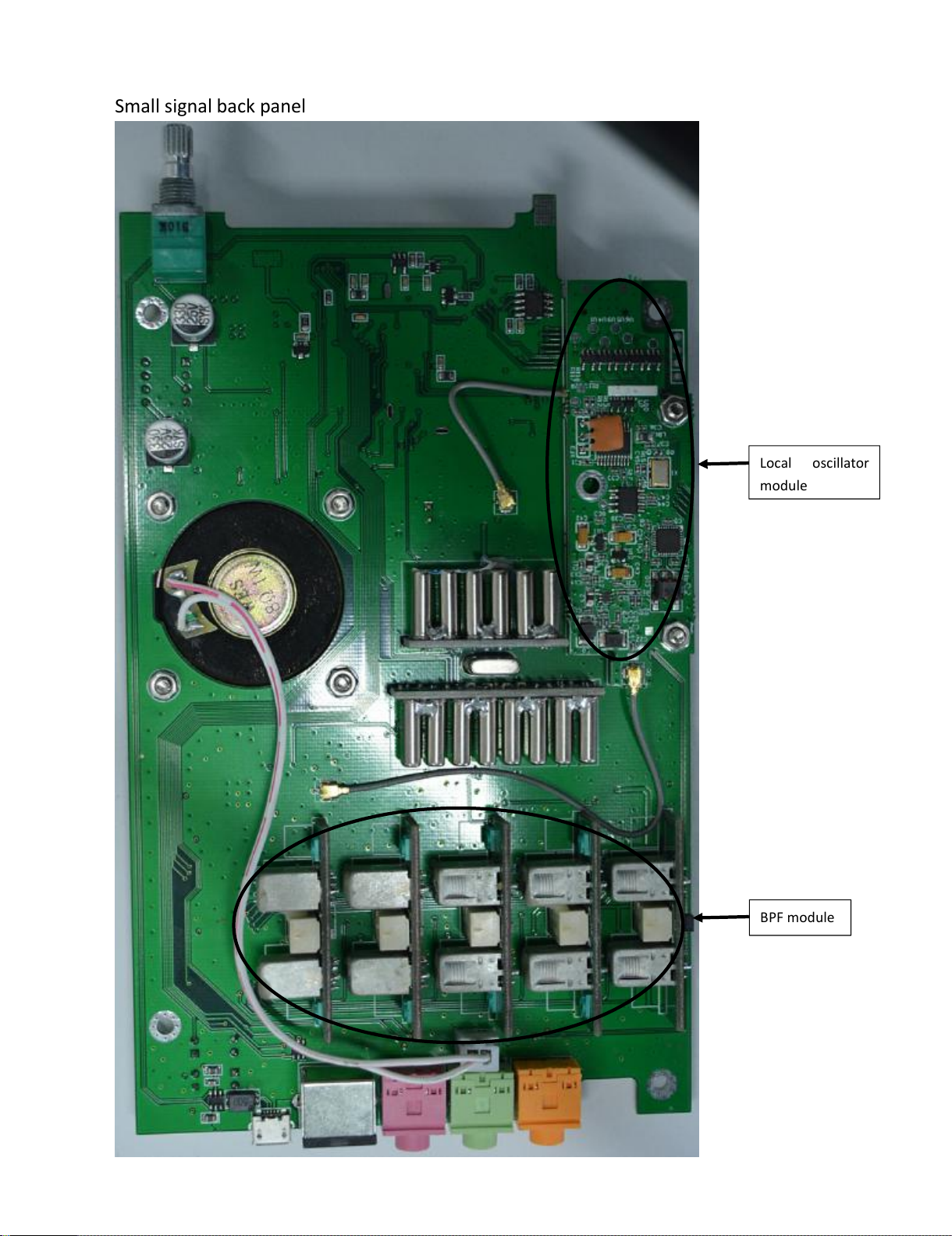
Band-pass filter consists of 5 modules (XGM1--XGM5),
it can make 10 amateur bands. U20, U21 are band
switching controller,connect the input band switching
signal to LPF unit switching relay of power amplifier
board.
Preamplifier is composed of Q7 and its periphery
circuit. Preattenuator is πType attenuator, which is
composed of R57、
R64、
R65. U4、
U12、
U15、
U18 are
RF switching trigger, to control the RX Signal trend.
PRE_EN and ATT_EN are control signals ,by these 2
control signals to control the signal to be passthrough
mode, amplifier mode, attenuator mode,
amplifier+attenuator mode.Q8 、Q9 are switching
control digital triode.
3.1.2 Receiving mixer
U5
(ADE-1)
is receiving mixer,
inside is diode balanced
mixing structure. The RX receiving signal is mixing 1st
LO here, to bring 10.7MHz IF signal.
D15 is LO input switch, it’s in forward conduction
status when receiving, the LO enters the mixer. D15 is
closed when transmitting.
3.1.3 IF PREAMP
After mixing, it brings a receiving 1st IF signal. This
signal enters IF preamplifier Q21 via transformer T7 to
finish the first IF amplify. This amplified IF signal
outputs to intermediate frequency crystal filter(IFCF)
by T5. Q6 is NB control switch which controls the
conducting of the Q21.
3.1.4 IFCF sets
The radio is builted-in with 3 sets of IFCF, they are SSB -
2.2k (XMD1), CW - 500Hz (XMD2), and AM - 7.5K (XF1).
Q1, Q11 and Q12 control the access of this three IFCF
respectively.
3.1.5 IF Two stage amplifier circuit
The IF two stage amplifier circuit is composed of Q13
and Q15, the IF signal which be input by T4 makes the
final IF amplification here then sent to the automatic
gain control unit and the demodulation unit.
The automatic gain control unit is composed of Q4, D1,
U1 and its peripheral devices. The automatic gain
control voltage is sent to the G2 pole of the two stage
IF amplifier respectively to receive automatic gain
control. The starting speed is switched by U1 and Q23,
and the switching signal is AGC-S.
The automatic gain control voltage outputs S table
signal after buffering and amplifying by U2.
3.1.6 Demodulator circuit
The demodulation of single sideband signal SSB and
continuous wave signal CW is accomplished by a
product detector which is composed of U6 (SA602).
The BFO signal is input through by the 6 pins to the
demodulator, and the demodulated audio signal is
output by 5 pins. By controlling the frequency of the
injected BFO signal, the demodulation of SSB and CW
modes can be completed.
Part 3 Circuit principle
All manuals and user guides at all-guides.com
all-guides.com

The demodulation of AM mode is accomplished by D2
and its peripheral circuit.
The demodulated SSB, CW and AM audio signals are
input to the U13 audio switcher then switch in
different modes and output.
3.1.7 Audio unit
The audio switcher U13 input an audio signal, this
signal is amplified by the active filter amplifier U7, then
amplified and output by an audio power amplifier U9
(LM386) to drive speaker.
3.1.8 Pulse noise blanking processor NB
Receiving an IF signal which is output by a mixer enters
the NB amplification/control unit after Q22 buffering,
this part is composed of U3, Q27, D47, Q29, Q34, Q30,
Q28 and Q6. When the pulse interference signal
strength exceeds the threshold, this circuit starts to
work, Q6 controls the IF preamplifier Q21 to be shutoff
to bring the noise elimination.
3.2 Transmitting circuit
3.2.1 Microphone amplifying circuit
The microphone amplifying circuit is located on the
power board, and consists of U15B and U17B. U15B
(SSM2167) has voice amplification and voice
compression function, and the compression ratio is
switched by U15B.
3.2.2 Modulator circuit
The microphone amplified signal enters the modulator
U6 via the audio switch U27 to do SSB modulation. AM
modulator circuit consists of U6, Q10, D3, D8 and so on,
to restore carrier and modulate.
3.2.3 Transmit 1 IF amplified / filtered circuit
The output signal of the debugger U6 is amplified by
Q25 and then enters the IFCF (XMD1, XMD2, XF1) for
filtering, then amplified by Q3 for the second time, and
output to the transmitting mixer by T8.
The CW_TXE signal is the transmit control enable signal
in the CW mode.
3.2.4 Transmitted mixer
T8 outputs a transmitting 1 IF signal which is sent to
the transmit mixer U10 (AD831) for mixing, then
output a final transmitting small signal by the 16 pin.
3.2.5 Transmit small signal filter/output switching
U10 outputs a small signal and this small signal is
filtered through the BPF module (XGM1 - XGM5), and
then output transmitting final small signal by a electric
switcher which is composed of D28 and D9, the
interface is P2 (U.FL socket).
R
9
9
2
.
7
k
R
8
9
2
.
7
k
C
8
2
1
0
0
n
F
C
1
0
6
1
0
0
n
F
L
3
0
1
0
0
u
H
L
3
7
1
0
0
u
H
C
8
7
1
0
0
n
F
C
1
0
0
1
0
0
n
F
+
9
R
+
9
T
P
1
U
.
F
L
插
座
P
2
U
.
F
L
插
座
D
2
7
M
A
2
Z
0
7
7
D
2
8
M
A
2
Z
0
7
7
C
7
3
1
0
0
n
F
L
2
2
1
0
0
u
H
R
1
3
1
2
.
7
k
D
9
M
A
2
Z
0
7
7
1
T
P
1
5
N
C
1
T
P
1
6
N
C
A
F
_
A
M
R
1
4
2
1
k
R
1
4
1
k
1
2
3
D
2
1
S
S
3
7
2
R
1
4
4
1
0
0
k
C
2
8
4
.
7
n
F
R
1
4
3
6
8
k
+
9
R
5
1
5
k
C
1
7
4
7
0
n
F
C
1
6
5
2
.
2
n
F
All manuals and user guides at all-guides.com

3.2.6 Power prime amplifier
P2 outputs a transmitting small signal, this small signal
is connected to the socket P4B on the power supply
board by IPEX wire, and it is prime amplified by Q5B
(2SC5551), then output by the T6B.
3.2.7 Power amplifier units
Power amplifier units are composed of Q4B 、Q3B 、
Q1B 、Q2B. Q1B and Q2B are final stage power
amplifier ,Push-pull amplifier are made up of 2pcs
RD16HHF1 ,stable output around 18W power signal.
T2B is final stage output transformer.
The bias voltages of each level power tubes are all
generated and supplied by a pedestal generator which
consists of Q7B and U6B.
3.2.8 Low pass filter
The 6 stage, 5th order elliptic low-pass filter which is
composed of relay and magnetic winding is responsible
for filtering and removing the spurious and harmonic
signals which are generated by the power amplifier,
and U3B, U4B and U9B control the band switching.
3.2.9 Power/Standing wave detector
The power/SW detector is composed of T1B, T7B, D1B,
D2B etc. It detects the output of antenna port and
reflected power, U5B buffs and amplify the tested
output signal, then sent to the microcontroller for
processing and display the power and SW value.
3.2.10 Automatic power control circuit
The forward power detection value and the setting
power value are sent into the U22A at the same time
to process automatic power control, and output VALC
voltage to control the amplification of the Q3, so as to
achieve the purpose of automatic power control.
3.3 Control unit / Interface circuit
3.3.1 Microprocessor unit
Microprocessor U17 controls the whole work of
the machine. Its I/O signal is mainly divided into
switching signals and digital signals.
Microprocessor comes with AD/DA converter. The
inside detection signal, such as S table, forward power
and back power, are input to inside the processor to
read by a special ADC port.
The microprocessor expands the I2C memory U8 to
store the related data information.
3.3.2 External interface circuit unit
X108G has the following external interfaces: AUX,
KEYER, ACC, SPK, Micro-USB.
Micro-USB is the real USB connector and it connects to
the processor U17.
Key interface KEYER is common interface for
manual/automatic key, connects to processor U17.
B
A
N
D
B
P
F
L
P
F
3
.
5
~
4
.
0
M
B
6
B
1
B
2
B
3
B
4
B
5
L
1
L
2
L
3
L
4
L
5
B
A
N
D
S
E
L
E
C
T
I
O
N
T
A
B
L
E
L
6
1
.
8
~
2
.
0
M
B
7
B
8
B
9
B
1
0
C
O
D
E
0
0
0
0
B
0
0
0
1
B
0
0
1
0
B
0
0
1
1
B
0
1
0
0
B
0
1
0
1
B
0
1
1
0
B
0
1
1
1
B
1
0
0
0
B
1
0
0
1
B
1
0
~
1
0
.
2
M
1
4
~
1
4
.
5
M
1
8
~
1
8
.
2
M
2
1
~
2
1
.
6
M
2
4
.
8
~
2
5
M
2
8
~
2
8
.
8
M
5
~
5
.
5
M
N
o
n
-
H
A
M
-
B
A
N
D
7
~
7
.
3
M
B
1
1
1
0
1
0
B
C
1
0
7
B
1
0
0
n
F
R
6
5
B
1
k
+
6
R
E
F
+
9
T
R
6
6
B
3
.
9
k
C
1
0
0
B
1
0
0
n
F
R
W
5
B
N
C
R
6
7
B
2
k
1
T
P
5
B
N
C
R
T
1
B
N
C
R
6
8
B
N
C
R
3
4
B
6
8
0
R
C
9
5
B
1
0
u
F
U
6
B
T
L
4
3
1
C
P
K
Q
7
B
B
C
8
6
8
All manuals and user guides at all-guides.com

SPK port is the external speaker interface, it connects
to the audio power amplifier U9.
ACC port is MIDI-DIN type 6 core data interface, which
extends the external PTT signal, band voltage, external
ALC input, external audio, +9V and GND ports.
AUX interface function is not open yet, the internal
connects to the RX/TX port of processor, can be
reserved as a backup serial port.
The band voltage generator consists of microprocessor
and U25 and U26.
3.4 Power unit
There are 2 groups main power supply for
X108G, 9V and 5V, which are generated by U1B
(LM2940T-9.0) and U2B (LM7805) on the power
amplifier board.
The microprocessor requirs 3.3V voltage which
is generated by the U19.
The local oscillator requires 3.3V and 1.8V voltages
which are generated by their BMP power supply.
Q9B and Q10B generates transmit-receive voltage +9R
and +9T.
The power switch is an electronic power switch which
is composed of Q6B and Q8B. PWR_SW is the control
signal of the power on/off.
C
1
5
7
1
0
0
n
F
B
A
N
D
_
V
O
L
T
U
2
6
7
4
V
1
G
1
4
C
+
5
P
W
M
_
O
U
T
U
2
5
M
C
P
6
0
0
1
U
C
1
8
8
1
0
0
n
F
+
5
R
1
6
9
1
k
C
1
8
9
4
7
0
n
F
All manuals and user guides at all-guides.com

Following the below debugging methods to adjust the parameters of the small signal board and the power amplifier
board to resume to default setting.
4.1 Machines
Machine
SPECS
Machine
SPECS
DC power supply
Output voltage: 13.8V
RF spectrum
analyzer
Frequency range: 0.1-1000MHz
Output current: maximum 10A
BW resolution ratio: 10Hz
It has perfect protection function
Audio
analyzer
SINAD analysis function
Audio frequency
generator
Output frequency: 100Hz-10kHz
Measuring range: 10mV-10V
Output amplitude: 1mV-1V RMS
Oscilloscope
Frequency range: DC-100MHz
RF signal
generator
Output frequency: 0.1-500MHz
Measuring range: 0.01-20V
Output amplitude: -127dBm-0dBm
Digital
multimeter
3 and a half
Digital ammeter
Measuring range: 0.001-10A
External
speaker
8Ω& 2W
All equipment has been measured and tested within the period of validity.
4.2 Small signal board debugging
4.2.1 The small signal board has used the network analyzer to adjust the channel to the predetermined status.
Please do not make any adjustments to the IF transformer on the channel, otherwise it will cause the
deterioration of the transmit-receive capability.
4.2.2 Receiving channel gain debugging
Required machines and its settings
Machine
Setting specs
RF signal source
Frequency: 14.251MHz, output amplitude: -97dBm
Oscilloscope
the units on the X-axis:1ms,
the units on the Y-axis:100mV
Note: During the test, do not turn-on the X108G to transmit, otherwise the RF signal source will be damaged!
1) Set the receiving frequency of X108G to be 14.25000MHz, [USB]mode.
2) Open [PRE],close [ATT] and [AGC] and [SQL].
3) Adjust the volume to be 1/3.
Part 4 Debugging
All manuals and user guides at all-guides.com

4) Signal source output a signal, connect it to the antenna interface of X108G.
5) Use oscilloscope to observe the signal amplitude of test point(signal frequency:1kHz).
6) Adjust the 2nd IF transformerT1 to make the range of magnitude observed on the oscilloscope is the largest
(normally it is more than 550mV-Vpp).
4.2.3 Receiving sensitivity test
Required machines and its settings
Machine
Setting specs
RF signal source
Frequency: 14.251MHz, initial output amplitude: 10uV
Audio analyzer
SINAD test
1) Set the receiving frequency of X108G to be 14.25000MHz, [USB] mode.
2) Open [PRE],close [ATT] and [AGC] and [SQL].
3) Connect the SPK interface to input port of audio analyzer.
4) adjust the volume of the X108G to make the amplitude of the signal measured by the audio analyzer is
2000mV.
5) Set the RF signal source output amplitude to be 0.35uV, and the SINAD test value of the audio analyzer
should be greater than 12dB, which is regarded as qualified.
Oscilloscope test
point
IF transformerT1
All manuals and user guides at all-guides.com
all-guides.com

4.2.4 NB unit test
Required machines and its settings
Machine
Setting specs
RF signal source
Frequency: 14.251MHz, output amplitude: -80dBm
Digital multimeter
DC voltage test
Note: During the test, do not turn-on the X108G to transmit, otherwise the RF signal source will be damaged!
1) Set the receiving frequency of X108G to be 14.25000MHz, [USB] mode.
2) Open [PRE],close [ATT] and [AGC] and [SQL].
3) Measure the voltage of NB unit test point with digital multimeter.
4) Adjust NB amplify IF transformerT16 to make the test point voltage to be minimum (around 1.55V).
5) Turn off the signal source output, and the voltage value of the test point is about 4.15V.
4.2.5 S table Parameter calibration
Required machines and its settings
Machine
Setting specs
RF signal source
Frequency: 14.251MHz
Note: During the test, do not turn-on the X108G to transmit, otherwise the RF signal source will be damaged!
NB unit test point
IF transformerT16
All manuals and user guides at all-guides.com

1) Set the receiving frequency of X108G to be 14.25000MHz, [USB] mode.
2) Open [PRE],close [ATT] and [AGC] and [SQL].
3) Connect the output port of the RF signal source to the antenna interface of the X108G;
4) Turn off the RF signal source output, adjust the S table reference voltage PotentiometerRW1, make the
-121dBm value of ADC on the screen is 2500, press the [SET] button to enter the next level signal setting.
5) Open the RF signal source, in turn, set up the signal source output signal amplitude by the each signal
intensity as displayed on a screen, and then press the [SET] button to enter the next level of signal
settings.
6) After setting all the signal levels, press the [SAVE] button to save and exit.
4.2.6 Overall gain adjustment of transmit channel
Required machines and its settings
Machine
Setting specs
Digital multimeter
DC voltage test
1) Set the receiving frequency of X108G to be 14.25000MHz, [CW] mode.
2) Pull out the TX signal plug of the small signal board.
3) Press the key to start the CW mode transmit.
4) Measure the voltage of the transmit gain test point TP11, and adjust the PotentiometerRW8 to make the
voltage of the test point be 2V + 0.1V.
PotentiometerRW1
All manuals and user guides at all-guides.com

4.2.7 Modulation audio signal amplitude adjustment
Required machines and its settings
Machine
Setting specs
Audio frequency generator
Frequency:1kHz Amplitude:100mV-Vpp
50W RF load
1) Set the receiving frequency of X108G to be 14.25000MHz, [USB] mode.
2) Connect the RF load to the antenna port of the X108G.
3) Unplug the TX signal line from small signal board to the power amplifier board.
4) Measure the amplitude of the test point TP10 with oscilloscope.
5) Press PTT of hand microphone, adjust PotentiometerRW4 to make the amplitude of test point be
50mV-Vpp.
4.2.8 SSB mode carrier suppression debugging
Required machines and its settings
Machine
Setting specs
Audio signal generator
Frequency:1kHz Amplitude:100mV-Vpp
Spectrum analyzer
Central frequency:14.25MHz BW:10MHz
50W RF load
Test point TP10
Potentiometer RW4
All manuals and user guides at all-guides.com

1) Set the receiving frequency of X108G to be 14.25000MHz, [USB] mode.
2) Connect the RF load to the antenna interface of the X108G.
3) Connect the TX output signal of the small signal board RF spectrum analyzer.
4) The output signal of the audio signal source is connected to a special test microphone,and open the
output of the audio signal source.
5) Press the PTT of speaker microphone to start the X108G transmitting, and observe the carrier output
power measured by the spectrum analyzer.
6) Adjust PotentiometerRW6to make the carrier power measured on the spectrum analyzer is minimum.
4.2.9 AM modulation debugging
Required machines and its settings
Machine
Setting specs
Audio frequency generator
Frequency:1kHz Amplitude:100mV-Vpp
Spectrum analyzer
Central frequency:14.25MHz BW:10MHz
50W RF load
1) Set the receiving frequency of X108G to be 14.25000MHz, [AM] mode;
2) Connect the RF load to the antenna interface of the X108G.
3) Connect the TX output signal of the small signal board RF spectrum analyzer.
4) The output signal of the audio signal source is connected to a special test microphone,and open the
output of the audio signal source.
5) Press the PTT of speaker microphone to start the X108G transmitting,and observe the power difference
between carrier and envelope which are measured by spectrum analyzer
6) Adjust PotentiometerRW5,to make he carrier power is higher than the envelope power 14dB + 1dB.
PotentiometerRW6
All manuals and user guides at all-guides.com

4.2.10 Transmit closed loop debugging
Required machines and its settings
Machine
Setting specs
Digital multimeter
DC voltage test gear
Spectrum analyzer
Central frequency:14.25MHz BW:5MHz
50W RF load
1) Set the receiving frequency of X108G to be 14.25000MHz, [CW] mode,power 20W
2) Connect the RF load to the antenna interface of the X108G.
3) Press the CW key to start the transmit, measure G2 voltage of the transmitting amplifier Q3 by digital
multimeter.
4) Adjust the IF transformerT8 to make the test voltage value be minimum.
PotentiometerRW5
IF
transformerT8
All manuals and user guides at all-guides.com
all-guides.com

4.2.11 Power amplifier unit static debugging
Required machines and its settings
Machine
Setting specs
Digital ammeter
DC voltage test gear
50W RF load
1) Set the receiving frequency of X108G to be 14.25000MHz, [USB] mode.
2) Unplug the TX signal line from small signal board to the power amplifier board.
3) Connect the RF load to the antenna interface of the X108G.
4) Disconnect R81B、R82B、R79B、R80B solder joints.
5) Connect a dedicated test microphone to X108(disconnect the microphone input), then press PTT to start
the transmitting, and record the current ammeter value as a baseline reading.
6) Solder four debug solder joints, adjust the corresponding Potentiometer, start the transmitting to make
the value of additional current are as follows:
Solder joints
Potentiometer
Additional current
R81B
RW4B
30mA
R82B
RW2B
250mA
R79B
RW1B
300mA
R80B
RW3B
300mA
Notes:
When debug a joint, other 3 joints must be cut off.
Must solder 4 test joints after debugging. Please cut off the radio power when soldering.
R80B
R79B
R82B
R81B
RW3B
RW1B
RW2B
RW4B
All manuals and user guides at all-guides.com

Power amplifier board
NO.
Item
SPECS
PACKAGE
BRAND
MPN
Designator
1
Aluminum
solid cap
100uF
Würth
875105359010
C1B, C2B, C7B, C8B, C90B, C110B,
C113B
2
capacitor
100nF
0603
Murata
GRM188R71H104KA93
C3B, C4B, C5B, C6B, C40B, C45B,
C46B, C56B, C59B, C60B, C61B, C62B,
C66B, C67B, C68B, C69B, C70B, C73B,
C74B, C75B, C76B, C77B, C81B, C82B,
C83B, C84B, C87B, C97B, C98B,
C100B, C102B, C105B, C106B, C107B,
C109B, C111B, C114B, C115B, C120B,
C130B, C133B
3
capacitor
100pF
0805
Murata
GRM21A5C2D101JW01
C9B, C10B, C18B, C21B, C24B, C47B,
C49B, C55B
4
capacitor
1nF
0805
Murata
GRM21AR72D102KW01
C11B, C19B, C63B, C64B, C79B, C80B
5
capacitor
330pF
0805
Murata
GRM21A5C2D331JW01
C12B, C28B, C31B, C36B
6
capacitor
680pF
0805
Murata
GRM21A7U2D681JW31
C13B, C15B, C27B
7
capacitor
470pF
0805
Murata
GRM21A7U2D471JW31
C16B, C17B
8
capacitor
1.5nF
0805
Murata
GRM21AR72D152KW01
C20B
9
capacitor
1.2nF
0805
Murata
GRM21A7U2D122JW31
C22B, C23B
10
capacitor
47pF
0805
Murata
GRM21A5C2D470JW01
C25B, C32B
11
capacitor
75pF
0805
Murata
GQM2195C2E750GB12
C26B, C52B
12
capacitor
30pF
0805
Murata
GQM2195C2E300GB12
C29B
13
capacitor
150pF
0805
Murata
GRM21A5C2D151JW01
C30B
14
capacitor
27pF
0805
Murata
GRM21A5C2D270JW01
C33B, C50B, C139B
15
capacitor
100nF
0805
Murata
GRM21BR72A104MAC4
C34B
16
capacitor
68pF
0805
Murata
GRM21A5C2D680JW01
C35B, C54B
17
capacitor
120pF
0805
Murata
GRM21A5C2D121JW01
C38B, C53B
18
capacitor
220pF
0805
Murata
GRM21A5C2D221JW01
C39B, C48B
19
capacitor
12pF
0805
Murata
GRM21A5C2D120JW01
C41B, C42B
20
capacitor
47nF
0603
Murata
GRM188R71H473KA61
C43B, C44B
21
capacitor
8.2pF
0805
Murata
GQM2195C2E8R2BB12
C51B, C136B
22
Aluminum
solid cap
10uF
Würth
875105359001
C57B, C58B, C95B, C145B
23
capacitor
1nF
0603
Murata
GRM1885C2A102JA01
C85B, C88B, C91B, C92B, C94B
24
capacitor
100pF
0603
Murata
GRM1885C2A101JA01
C86B, C89B, C112B
25
capacitor
470nF
0603
Murata
GRM188R71C474KA88
C93B, C116B, C121B
26
capacitor
33pF
0805
Murata
GRM21A5C2D330JW01
C96B, C124B
27
capacitor
10uF
0805
Murata
GRM21BR61E106MA73
C117B, C118B
28
capacitor
20pF
0805
Murata
GQM2195C2E200GB12
C127B, C128B
29
capacitor
10nF
0603
Murata
GRM188R71H103KA01
C129B
Part 5 Parts List
All manuals and user guides at all-guides.com

30
capacitor
22pF
0805
Murata
GRM21A5C2D220JW01
C134B
31
capacitor
82pF
0805
Murata
GRM21A5C2D820JW01
C138B
32
Schottky
diode
1SS372
SC-70
Toshiba
1SS372
D1B, D2B
33
Zener diode
10V
SOD-323
Changjiang
Electronic
BZT52C10V0S
D3B, D4B, D16B
34
diode
1N4007
DO-214AC
domestic
M7
D5B
35
Zener diode
5.1V
SOD-323
Changjiang
Electronic
BZT52C5V1S
D6B
36
diode
1N4148
SOD-323
domestic
T4
D7B, D8B, D9B, D10B, D11B, D12B,
D13B, D14B, D15B, D17B
37
TVS diode
array
NUP2201MR6T1G
TSOP-6
ON
NUP2201MR6T1G
D18B
38
relay
HRB1-S-DC5V
Through-Hole
HKE
HRB1-S-DC5V
K2B, K3B, K4B, K5B, K6B, K7B, K8B,
K9B, K10B, K11B, K12B, K14B, K15B
39
Magnetic
inductance
T37-2
Through-Hole
HOMEMA
DE
-
L1B, L2B
40
Magnetic
inductance
T37-2
Through-Hole
HOMEMA
DE
-
L3B, L4B
41
Magnetic
inductance
T37-2
Through-Hole
HOMEMA
DE
-
L5B, L6B
42
Magnetic
inductance
T37-2
Through-Hole
HOMEMA
DE
-
L7B, L8B
43
Magnetic
inductance
T37-2
Through-Hole
HOMEMA
DE
-
L9B, L10B
44
Magnetic
inductance
100uH
0805
TDK
GLF2012T101K
L11B, L15B, L16B, L17B, L18B, L19B
45
Magnetic
inductance
T37-2
Through-Hole
HOMEMA
DE
-
L13B
46
Magnetic
inductance
T37-2
Through-Hole
HOMEMA
DE
-
L14B
47
Power
inductance
4.7uH
WE-PDF_104
5
Würth
7447797470
L20B
48
Magnetic
beads
600R
0805
Würth
74279204
LB1B, LB2B, LB4B, LB5B, LB6B, LB7B,
LB8B
49
Magnetic
beads
600R
1812
Würth
742792514
LB10B
50
RF connector
U.FL socket
SMT
MOLEX
73412-0114
P3B, P4B
51
FPC
connector
40 pins
0.5mm spacing
SMT
HRS
FH33-40S-0.5SH
P5B
52
Connector
RJ45
ZXCNT
-
P7B
53
RF FET
RD16HHF1
T-30E
Mitsubishi
RD16HHF1
Q1B, Q2B
54
RF FET
RD06HHF1
T-30E
Mitsubishi
RD06HHF1
Q3B
55
RF FET
RD01MUS1
SOT-89
Mitsubishi
RD01MUS1
Q4B
56
Triode
2SC5551
SOT-89
Mitsubishi
2SC5551
Q5B
All manuals and user guides at all-guides.com

57
FET
FDS4435BZ
SO-8
FAIRCHILD
FDS4435BZ
Q6B, Q8B
58
RF FET
BC868
SOT-89
Philips
BC868
Q7B
59
FET
IRLML5203PBF
SOT-23
IR
IRLML5203PBF
Q9B, Q10B
60
Digital triode
DTC114EKA
SOT-23
ROHM
DTC114EKA
Q26
61
Resistance
51R
1206
Yageo
RC1206FR-0751R
R1B, R2B
62
Resistance
330R
0603
Yageo
RC0603FR-07330R
R3B, R15B, R17B
63
Resistance
330R
1812
Yageo
RC1812FR-07330R
R4B, R11B
64
Resistance
1k
0603
Yageo
RC0603FR-071K
R5B, R12B, R14B, R16B, R30B, R47B,
R51B, R65B
65
Resistance
3.3R
0603
Yageo
RC0603FR-073R3
R6B, R10B
66
Resistance
220R
1206
Yageo
RC1206FR-07220R
R7B
67
Resistance
220R
0603
Yageo
RC0603FR-07220R
R8B
68
Resistance
220R
1812
Yageo
RC1812FR-07220R
R9B
69
Resistance
0603
Yageo
RC0603FR-07
R13B
70
Resistance
1.5k
0603
Yageo
RC0603FR-071K5
R18B
71
Resistance
4.7R
1206
Yageo
RC1206FR-074R7
R19B
72
Resistance
10k
0603
Yageo
RC0603FR-0710K
R20B, R23B, R32B, R33B, R35B, R36B,
R49B
73
Resistance
5.1k
0603
Yageo
RC0603FR-075K1
R21B, R41B
74
Resistance
5.1R
0603
Yageo
RC0603FR-075R1
R22B, R26B
75
Resistance
1.8k
0603
Yageo
RC0603FR-071K8
R24B, R25B
76
Resistance
680R
0603
Yageo
RC0603FR-07680R
R27B, R34B
77
Resistance
150R
0603
Yageo
RC0603FR-07150R
R28B
78
Resistance
100k
0603
Yageo
RC0603FR-07100K
R29B, R31B, R42B, R45B
79
Resistance
15k
0603
Yageo
RC0603FR-0715K
R43B
80
Resistance
100R
0603
Yageo
RC0603FR-07100R
R44B, R46B, R48B
81
Resistance
30k
0603
Yageo
RC0603FR-0730K
R50B
82
Resistance
0603
Yageo
RC0603FR-07
R52B
83
Resistance
3.3k
0603
Yageo
RC0603FR-073K3
R54B
84
Resistance
51R
0603
Yageo
RC0603FR-0751R
R55B
85
Resistance
35k
0603
Yageo
RC0603FR-0735K
R56B
86
Resistance
175k
0603
Yageo
RC0603FR-07175K
R58B
87
Resistance
75k
0603
Yageo
RC0603FR-0775K
R59B
88
Resistance
3.9k
0603
Yageo
RC0603FR-073K9
R61B, R62B, R63B, R64B, R66B
89
Resistance
2k
0603
Yageo
RC0603FR-072K
R67B
90
Resistance
0603
Yageo
RC0603FR-07
R69B
91
Network
Resistor
100k
8P4R
Yageo
YC164-JR07100K
RP1B, RP2B
92
Adjustable-re
sistance
5k
3X3 SMT
domestic
-
RW1B, RW2B, RW3B, RW4B
93
Magnetic
inductance
74270176
Through-Hole
HOMEMA
DE
-
T1B, T7B
94
Transformer
7427056
Through-Hole
HOMEMA
DE
-
T2B
95
Magnetic
BN-43-302
Through-Hole
HOMEMA
-
T3B
All manuals and user guides at all-guides.com
Other manuals for X108G
4
Table of contents
Other XIEGU Transceiver manuals