Alto SR400A User manual

Service Manual
ALTO
REV.2
Model: SR400A

CONTENTS
1.Specifications
2.Block Diagram
3.Schematic Diagram
4.Printed Circuit Board
5.Test Procedures
6.Structural Drawing
7.Exploded View & Mechanical Parts List
8.Electrical Parts List

Test Result
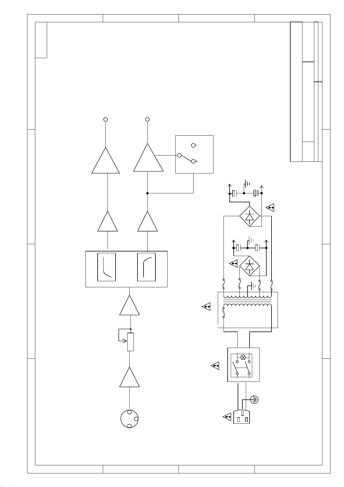
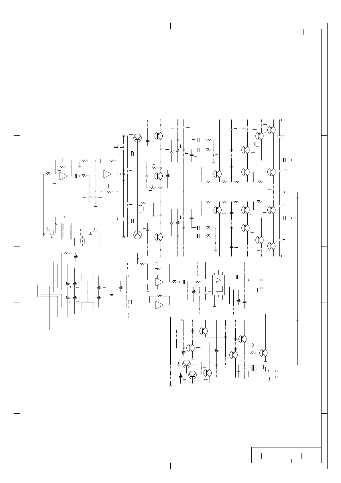
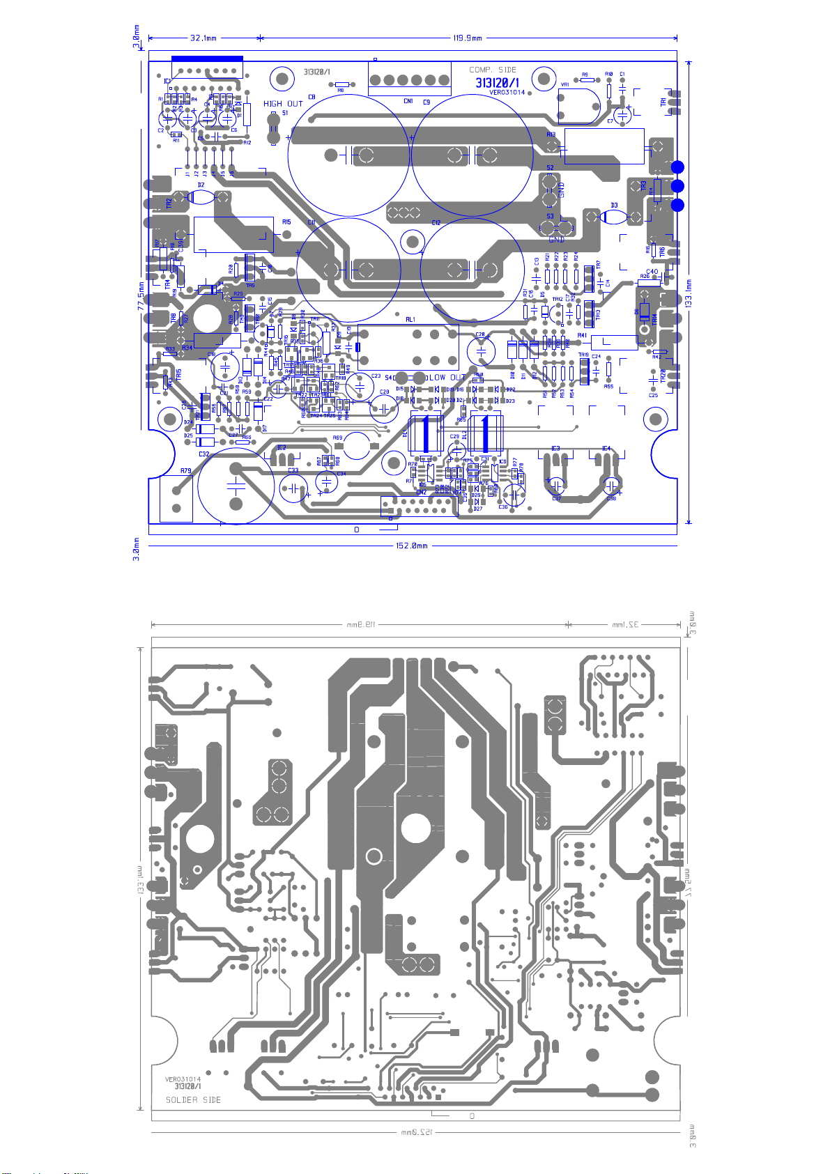
Model No: SR400A Test Date: 20040916 Tester: MO GUO ZHU
Test Item Test Conditions Spec Test Result Remark
1Power Source AC: 230V;50 Hz
2Idle Current AC 230 V No-Load 5 ±0.5 mV mV across R13 &R15
3Power
Consumption Rated Output.
Aux At 1KHz A
WA
WFLAT
4Rated Output Low Load :4Ω30---31 V THD:0.4↓V
Hi Load :8Ω18----19 V THD:0.8↓_______V
Load 16Ω V_______V
Load ____Ω (25V )VV
Load____Ω (50V )VV
Load____Ω (70V )VV
Load____Ω (100V )VV
Aux At 1KHz FLAT.
Rated W
5Maximum at
Output 10% THD Aux 1KHz dB
Load ΩWWFLAT
7Hum or Noise VR Line Max(Low ) 7↓ mV mV DSP OFF
VR Line Max (Hi ) 7↓ mV mV DSP OFF
8
100HZ:
dB 100HZ: dBTone control
Response Input From Aux
Output At 1W 10KHZ: dB 10KHZ: dB
9Puncture Voltage 5mA ,5Sec 3750V V
10 MONITOR Aux 1KHz dB Load ΩFLAT
MONITOR NO: AUX,TAPE,TUNER,CD,MIC1,MIC2
CD PLAYER 1KHz 0dB
TUNER AM/FM
PRIORITY MIC1
TEL.PAGING 1KHz____dB
Load____Ω_______V G-T___dB;
G-R___dB。G-T___dB;G-R___dB。FLAT
ZONE PAGING 100V ALL/ Z1,
Z2,Z3,Z4
AC : OUTPUT
REMOTE AC OUT or DC OUT
SPECIFICATIONS
01-1

Test Result
Model No:SR400A Test Date: Tester:MO GUO ZHU
Test Item 1. Input
Sensitivity 2. Signal/Noise 3. Distortion at
1W 4. Distortion at
Rated 5. Frequency
Response
Test Conditions
Test Result
FLAT Rated
Output 30V/18V
Load 4Ω/8Ω
FLAT Rated
Output 30V/18V
Load 4Ω/8Ω
FLAT Output
at 2V Load 4ΩFLAT Rated
Output 30V/18V
Load 4Ω/8Ω
FLAT Output at
1WREF-3dB
Load 4Ω
Low OUT -9 ±0.5 dBV70↑ dB 0.5↓% 0.4↓ % 22Hz~22KHz↑
Hi OUT -8±0.5 dBV68↑ dB 0.5↓% 0.8↓ % 25Hz~22KHz↑
TUNER dB dB % %
LINE
CD dB dB % %
AUX dB dB % %
TAPE dB dB % %
TUNER dB dB % %
AUX2
CD dB dB % %
AUX dB dB % %
TAPE dB dB % %
TUNER dB dB % %
AUX3
CD dB dB % %
LOW -50±0.5 dBV60↑ dB 0.8↓ % 0.3↓ % 22Hz~22KHz↑
HI -50±0.5 dBV60↑ dB 0.5↓% 1↓ % 25Hz~22KHz↑
24V dB dB % %
MIC
UNBAL dB dB % %
MIC dB dB % %
LINE dB dB % %
24V dB dB % %
MIC-2
UNBAL dB dB % %
MIC dB dB % %
LINE dB dB % %
24V dB dB % %
MIC-3
UNBAL dB dB % %
MIC dB dB % %
LINE dB dB % %
24V dB dB % %
MIC-4
UNBAL dB dB % %
Remark
1. When the above itemsare tested, short circuit the 1st and the 2nd pin of 313115-1 (DSP) CN1. After the
test, remove the short circuit terminal.
2.Load connection: connect LOW output with 4Ohms, and connect HIGH output with 8Ohms.
3. Please check if the bass BOOST circuit is OK. If bass output is below 18V(ON LOAD), BOOST
circuit does not operates. If bass output is above 18V(ON LOAD), BOOST circuit starts operation.
4. FR test: use AP to scan DSP ON and DSP OFF respectively. Refer to the attached figure for frequency
response curves.
Authorization by:Check by:
SPECIFICATIONS
01-2

1234
A
B
C
D
4321
D
C
B
A
POWER SWITCH
MIX AMP PRE AMP
HI PRE
LOW PRE LOW POWER
HI POWER
AMP
AMP
AMP
AMP
LOW
V+ & V- V+ & V-
HI
POWER SUPPLY
SWITCH
LOW SPEAKER
HI SPEAKER
LOW V+
LOW V-
HI V-
HI V+
AC INPUT
238094
DSP MODULE
HPF
LPF
Title
Size:
A3
Number
Date:
File: Sheet of:
Drawn By:
Revision
SR400A
SR400A BLOCK DIAGRAM
SR400A 1/1
MO GUO ZHU
VER1.0
1
第 版
SR400A BLOCK DIAGRAM
SIGNAL INPUT
VOLUME
130 deg SW
T6.3A
T6.3A
T6.3A
T6.3A
02-1

12345678
A
B
C
D
87654321
D
C
B
A
2
1
3
4
MIC2
CN-BAL-MALE
ZD5
12V1W
ZD2
12V1W
ZD4
12V1W
ZD3
12V1W
R16
15K
R19
15K
R18
15K
R15
15K
R14
390E
1
2
3
+
_IC3A
33079 7
6
5+
_IC3B
33079
8
9
10 +
_
IC3C
33079
14
13
12 +
_
IC3D
33079
C23
22P
C20
22P
C19
22P
C26
22P
C27
0.01uF/400V
R22
10E
1
2
3
SW2A
SW PS-22E85L
4
5
6
P
SW2B
SW PS-22E85L
GND
1
2
3VR1
D50K
R17
4.7K
R21
820E
8
9
10 +
_IC1C
33079
C16
0.0033u
R12
10K
R10
10K
7
6
5+
_IC1B
33079
C5
0.0033u
R7
10K
R2
10K
R11
6K8
R1
6K8
C21
47u/63V
C22
47u/63V
C2
47u/63V
C1
47u/63V
1 2
3 4
5 6
7 8
910
1112
1314
1516
1718
1920
CN2
CN-10PX2-180
12
34
56
78
910
1112
1314
CN1
CN-7PX2-F
C17
47u/63V
1
2
3
+
_IC1A
33079
C7
22P
R4
10K
R5
10K
C6
0.0033u
R3
6K8
14
13
12 +
_
IC3D
33079
1
3
2
DL1
SIGN/LIMIT
R9
1K2
+15V
-15V
+5VD
+15V
-15V
NC 1
OUT 2
NC 3
GND
4GND
5
NC 6
V+ 7
NC 8
NC 9
FB
10
FC
11
GND
12 GND
13
OSC
14
SS
15
NC 16
IC2
L4962
C4
220u/63V
C9
330P
C12
0.0022u
R8
3K9
R6
15K
C8
0.033u
C13
2u2 100V
4
3
2
1
5
L1
TP-SEV1924-03
C25
470u/25V SLL*
C24
1000u/6V3
+5VD
D1
BYV27
R13
330E
11 4
IC1E
33079
11 4
IC3E
33079
C14
470u/25V SLL
C10
470u/25V SLL
C15
0.1u
C11
0.1u
+15V
-15V
CLIP
SIGNAL
R
G
X1X2
X3
1
2
3
4
5
6
MIC1
XLR
+5VA
HIGH
LOW
FROM INPUT TO 313115-1 DSP BOARD
HIGH INPUT
+4dB
L2
FL5R
L3
FL5R C28
10u/63V
C18
10u/63V
C29
10u/63V
SW1
0E
Title
Size:
A3
Number
Date:
File: Sheet of:
Drawn By:
Revision
SR400A
P-110018-SR400A
2004/08/27
SR300A 1/1
MO GUO ZHU
VER1.0
TO 313120-1 AMP PCB
1第 版
03-1

1 2 3 4
A
B
C
D
4321
D
C
B
A
F1
T6.3A
F3
T6.3A
F4
T6.3A
F2
T6.3A
D1 KBPC25
D4
GBU8D
D2
1N4002
C2
0.01uF400V
C1400V/10N
S1
S4
S3
S5
S2
+VCC1
-VCC1
+VCC2
-VCC2
Vac
KBU806
BP25-06PWS
Title
Size:
A4
Number
Date:
File: Sheet of:
Drawn By:
Revision
SR400A
P-313121-1
2004/08/27
SR300A 1/1
MO GUO ZHU
VER1.0
1
第 版
黃
橙
藍
紫
棕
03-2

1234
A
B
C
D
E
F
G
H
4321
H
G
F
E
D
C
B
A
R27
390E
R33
1K
R59
68K
R39
4K7
R40
12K
R31
470E
R23
820E R24
68E
R22
12K
R21
8K2
R52
8K2
R51
47E
R53
47K
R17
2K2
R55
1K
R32
12K
R18
470E
R20
12K
R9
560E
R10 1K5
R56
8K2
R58
47E
R66
8K2
R57
12K
R28
68E
R25
820E
R44
68K
R29
12K R46
4K7
R42
390E
R16
470E
R43
2K2
R59
47K
C17
220P
C24
470P
C21
470P
C23
0.0047U
C15
100P
C1
0.001U
C25
0.0047
C14
100P
TR9
NJE350
TR13
MJE350
TR7
MJE340
TR5
MJE340
TR12
2N5401
TR10
2N5551
D11
1N4002
TR1
MJE802
R34
8K2 2W
D10
7V5 1W
D14
7V5 1W
C18
220U/25V
D13
1N4002
D25
1N4002
D17
1N4002
D12
1N4002
VR1 470E
C25
10/50V
TR21
MJE340
TR15
NJE15031 TR8
TIP36C
TR4
MJE15030
TR2
2SC5200
R17
10E
R19
4E7
D24
1N4002
D4
1N4002
D14
6A2
C16
0.1U
TR19
MJE350
TR6
MJE15031
TR20
MJE15030
TR3
2SA1943
TR14
TIP35C
D5
1N4002
D3
6A2
R60
47K
R64
4K7
R63
10K
R8
47K
D17
1N4148
TR23
BC847
TR24
BC847
TR22
BC847
TR25
BC857
TR18
BC857
TR11
BC32725
TR17
BC857
C28
1000U/6V3
C23
220U/50V
R48
330E
R35
10K
R49
33K
R47
10K
R61
10K
R62
10K
R37
470E
R36
10K
R46
150K
C22
1U/50V
C7
0.1U
C13
0.0047U
R41
8K2 2W
C20220U 25V
R15
0E2 5W
R13
0E2 5W
C10
220P
D5
1N4148
D7
1N4148
R14
10E
R26
4E7
C27
0.0047U
7
6
5+
_IC6B
MC33078
1
2
3
48
+
_
IC6A
MC33078
1
2
3
48
+
_
IC5A
MC33078
7
6
5+
_IC5B
MC33078
R78
15K
R77 22K
R80
1K
R76
1K
R75
47K
R74
100K
R71
15K R70 47K
R73
10E
R11
10K
DL2 47P
C35 33P
C31
4N7
C3
22UF/50V
C4
10UF/50V
C6
10UF/50V
D27
4148 D26
4148
DL1 47P
MUTE
ST-BY
1
2
3
4
5
6
78
9
10
11
12
13
14
15
IC1
TDA7294
R3
22K
R4
1K
R21
10K
R32
33K
R12
22K
R1
22K
R12
10E 0.5W
C5
0.1U
D1
4148
R2
680E
+VCC1
-VCC1
+VCC1
-VCC1
+VCC2
-VCC2
Vin
1
GND
Vout
IC3 7915
Vin
1
GND
2
Vout 3
IC4 7815
C11
10000/50V
C12
10000/50V
C36
10/25V
C37
10/25V
1
2
3
4
5
6
CN1
6P/P=3.96
C8
10000/63V
C9
10000/63V
Vin
1
GND
2
Vout 3
IC2 7805
C33
1000U 6.3V
R79
47E/5W C32
2200U/63V
+VCC1
-VCC1
+VCC2
-VCC2
-15V
+5VA
+15V
-15V
+15V
-15V
+15V
-15V
D8
1N4148 TR16
BC857
R30
10K
-15V
R69
100E PTC
+15V
C39
330P
C40
330P
or NJL21184
or SIMILAR
or MJL21193
+15V
C36
10U NP
C2
1U 50V NP
TDA7294
12
34
56
78
910
11 12
13 14
CN2
CN-7PX2-F
+15V
RL1
OZ-SS-124LM1
DC 24V 16A
+5VA
-15V
S1
HIGH OUT +
S2
GND
S4
LOW OUT+
S3
GND
Hi SPEAKER
LOW SPEAKER
Title
Size:
A2
Number
Date:
File: Sheet of:
Drawn By:
Revision
SR400A
P-313120-1-SR400A
2004/08/27
SR300A 1/1
MO GUO ZHU
VER1.0
1第 版
FROM 110018 INPUT PCB
SOFT START
OFFSET PROTECTION
-7.7V
14.9V
8.84V
14.2V
9.4V
8.6V
0.2V
-0.5V
0.6V
20.2V
7.6V
24V
-24V-20.2V
-7.6V
-0.34V
-1.4V
+1.4V
D21
27.0K
1
2
DL2
TO POWER LED
03-3

04-1

TOPLAYER&TOPOVERLAY
BOTTOMLAYER
04-2

04-4

04-3

Instruments required:
1) Sinusoidal signal generator, 5) Resistive load 4 Ω 800W,
2) Dual trace scope, with probe, 6) Resistive load 8Ω 300W
3) Digital multimeter, 7) Pink noise from the GM “AUDIO CD”.
4) Variac 0-250 Vac,
P.S: Isolate the oscilloscope from earth and adjust the two traces on center of screen in GND
position.
Par. 1: visual check
-Make a visual check if the amplifier is perfectly done and especially verify:
a) the right value of fuses 6.3A 250V *4PCS
b) the right earth main connection on rear surface of front panel.
c) the insulation between the heat-sink and the case of TR1-15, IC1, 2, 3, 4-then,
-Set the VOLUME control full clockwise.
Par. 2: connections
-Switch off the amplifier module,
-Set the ENCODER pot. on preset “NORMAL”.
-Connect the mains of amplifier module to VARIAC and set it at zero AC voltage.
-Connect the signal generator to Line Input (XLR socket) and set it at 500Hz, 0dB .
-Connect the scope CH1 probe to amplifier low output and CH2 probe to amplifier high output-
Par. 3: Initial test
-Increase slowly the VARIAC voltage up to the nominal value (230Vac).
-Check the transformer sec. voltages with multimeter, (without signal on input):
S1-S2: 90V ±1.5Vac
S4-S5: 47V ±1.5Vac
-Check the +/-15Vdc supply on relative voltage regulator outputs (IC3 & IC4 devices).
-Switch ON the signal generator and verify that the output signals must be symmetrical referring
to GND, without detectable distortion and oscillation.
-Check that the low amplifier power output signal is 28+2VPEAK (19.5VRMS).
--Check of SIGNAL led function, moving the volume potentiometer of amplifier;
when the output signal is <0.5Vpeak the led must be OFF,
when the output signal is > 0.5Vpeak, the led must be GREEN lighted.
-Then, rotate the volume potentiometer knob full clockwise
Par. 4: BOOSTER check of LOW Amplifier
-Connect alternatively the CH2 probe tip of scope on D2 cathode and D3 anode and
verify the following conditions:
when the output signal is < 18Vrms the ±VCC1 voltage must remain linear at 28V,
when the output signal is > 18Vrms the ±VCC1 voltage must follow the output signal wave with
4Vdc offset, as shown in the following picture
05-1

TESTING PROCEDURE
-Switch ON the LOW amplifier output to 4Ω load resistor and repeat the above booster check
verifying more or less the same ± VCC1 conditions and verify that the signal must be
symmetrical refer to GND, without detectable distortion and oscillation.
Increase the VOLUME pot. until a signal clipping.
Switch OFF the LOW amplifier out. to 4Ω load resistor
Par. 5: COMPRESSOR check of LOW amplifier
-Increase the input signal of 10 dB and check the out. signal to remain constant at 45Vpeak and
if the Signal/Comp. led has changed the lighted colour, from GREEN to RED.
Par. 6: PTC function check on Heatsink
-Heat the PTC temperature sensor with a welder heated tip, in touch with its body, to verify this
protection works properly reducing the amplifier out. signal to few volts on time.
P.S. The check must be done with PTC, placed into heat-sink hole and silicon grease on.
Par. 7: Idle current setting of LOW amplifier
-Decrease to zero the signal generator, then, adjust VR1 trimmer to have a 5mV ±0,5mVdc
voltage drop across R13 & R15 (0,22Ω) power resistors.
Par. 8: HIGH amplifier check .
-Select a 10KHz frequency with 0dB amplitude on signal generator.
-Connect CH2 probe tip of scope on HIGH amplifier output.
-Check that the high amplifier power output signal is 26+2VPEAK (18VRMS).
-Switch ON the HIGH amplifier output to 8Ω load resistor and increase the VOLUME pot. -
Verify the out. signal is limited to 22Vpeak.
-Switch OFF the HIGH amplifier output to 8Ω load resistor.
Part .9: Burn-in test
1. Connect the pink noise signal from CD player with the line input of speaker module.
2. Connect 4ohm 500W load resistor with the bass output.
3. Connect 8ohm 300W load resistor with the treble output.
4. Put band switch to the position 1, and then turn on the power switch of speaker module.
5. Adjust the pink noise level from CD player untilSIGNAL/LIMIT indicators (red, green) sparkle.
6. Put the speaker module vertical and take the burn-in test for 2 hours.
Part .10: Final inspection
1. Check the electronic performance of the tested unit completely.
05-2

DSP OFF Frequency Response Curve of SR400A Speaker Module
Test Condition
1. Short circuit 2P pins of CN1 on DSP board (313115-1 board )
2. LINE INPUT : 1kHz;
LOW output :2V (4Ohm)
3. The upper curve is for treble output frequency response and the lower one is for bass output frequency response.
05-3

05-4

06-1

06-2

06-3

07-1
Table of contents
Other Alto Speakers System manuals