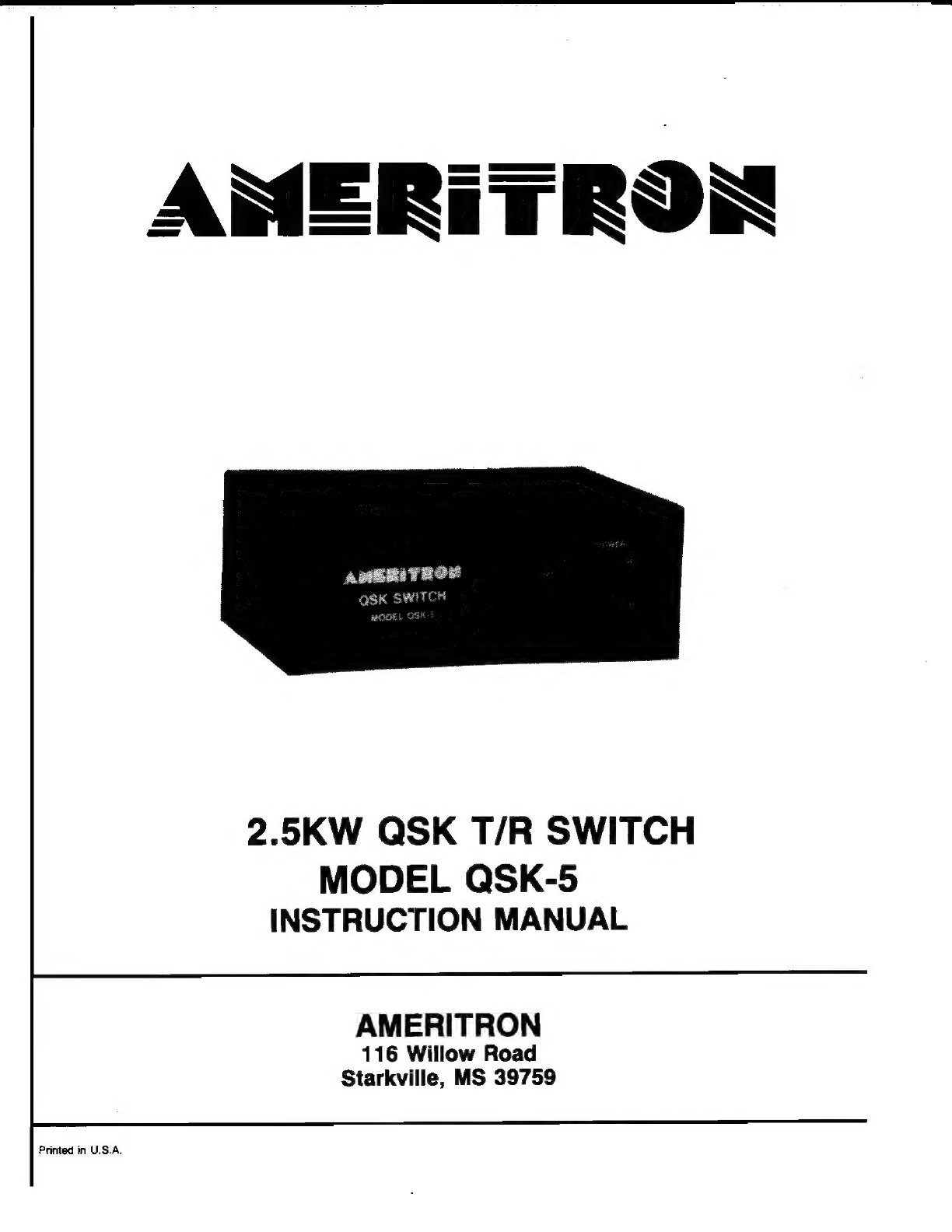
AMERITRON QSK-5 User manual

2.5KW
QSK
T/R
SWITCH
MODEL
QSK-5
INSTRUCTION
MANUAL
AMERITRON
116
Willow
Road
Starkville,
MS
39759


QSK-5
T/R
SWITCH
The
Ameritron
QSK-5
is
a_
self
contained
QSK
switch
that
adapts
non-QSK
amplifiers
to
full
break-in
operation.
The
QSK-5
is
housed
in
an
RF
shielded
enclosure
and
oper-
ates
on
120
VAC
power
lines
(QSK-5X
operates
on
200V
-
240V).
Inter-
face
connections
are
made
on
the
rear
panel
through
four
standard
phono
jacks
for
control
and
four
$0-239
connectors
for
RF.
The
QSK-5
will
handle
2000
watts
of
carrier
on
CW
and
2500
watts
PEP
on
SSB
in
normal
amateur
service
when
the
load
has
a
low
SWR.
An
optional
fan
is
required
for
continuous
carrier
modes
such
as
RTTY
and
Packet
at
power
levels
over
750
watts.
Internal
modifications
are
not
required
with
linear
amplifiers
that
use
less
than
25
volts
of
positive
polarity
on
the
"keying"
jack.
The
following
requirements
must
be
met
by
the
station
equipment
(amplifier,
antenna,
transceiver)
to
insure
proper
operation
of
the
QSK-5:
AMPLIFIER
REQUIREMENTS:
The
Ameri-
tron
QSK-5
(QSK-5X)
is
compatible
with
all
Ameritron
HF
Amplifiers.
The
keying
voltage
of
the
amplifier
used
with
the
QSK-5
must
be
a
positive
polarity
below
25
volts.
Most
popular
amplifiers
will
meet
this
requirement.
The
QSK-5
is
designed
to be
used
with
full
legal
limit
amateur
amplifiers
and
will
safely
carry
power
levels
up
to
2000
watts
on
CW
and
2500
watts
PEP
on
SSB.
The
SSTV,
RTTY
and
PACKET
rating
of
the
QSK-5
is
750
watts
average
power
with
5
minute
on
and
two
minute
off
duty
cycles
without
a
cooling
fan.
The
amplifier
output
rating
on
high
duty-cycle
modes
can
be
extended
to
1500
watts
with
the
optional
cooling
fan
installed.
ANTENNA
REQUIREMENTS:
The
antenna
SWR
must
be
low
if
the
QSK-5
is
operated
at
full
ratings.
To
calculate
the
safe
power
capability
of
the
QSK-5
use
the
following
formulas:
2800
divided
by
the
SWR
for
SSB
and
high
peak
to
aver-
age
power
modes.
2250
divided
by
SWR
for
CW
and
high
average
to
peak
power
modes.
1800
divided
by
SWR
for
RTTY
and
other
high
duty-
cycle,
high
average
power
modes.
NEVER
EXCEED
2000
WATTS
ON
CW,
2500
WATTS
ON
SSB
OR
1500
WATTS
ON
RTTY.
The
following
are
some
typical
SWR
values
and
power
ratings:
SWR
SSB
cw
RTTY
7:1
2500W
2000W
1500W
1.5:1
1875W 1500W
1200W
2.0:1
1400W
1125W
900W
3.0:1
950W 750W
600W
TRANSCEIVER
REQUIREMENTS:
The
QSK-
5
internal
relays
bypass
the
QSK-5
when
it
is
turned
off
or
if
trans-
missions
have
not
teen
made
within
the
previous
three
seconds.
This
bypass
feature
allows
the
QSK-5
to
be
removed
from
the
circuit
for
tuning,
normal
VOX
operation,
and
other
times
when
QSK
is
not
de-
sired.
It
also
allows
the
amplifier
to
have
a
cool
down
period
between
transmission
periods.
The
factory
wiring
of
the
QSK-5
gives
the
user
flexibility
in
the
choice
of
trans-
ceivers
and
allows
tailoring
the
QSK-5
to
almost
any
application.

RX
FUSE
LAMPS
AMP
OUT
ANTENNA
© ©
KEY
1
KEY
2
°
co
.
AMP
RELAY
O
AMERITRON
AUX
STARKVILLE,MS
MADE
IN
USA
BACK
PANEL
RF
INTERCONNECTIONS
AMP
OUT:
This
SO-239
connector
should
be
connected
to
the
RF
output
of
the
amplifier
with
a
short
length
of
good
guality
coax.
This
is
also
one
of
the
places
to
locate
a
TVI
low-pass
filter.
ANTENNA:
This
S0O-239
connector
connects
to
the
station
wattmeter.
The
antenna’
switch,
tuner,
or
antenna
must
follow
the
wattmeter.
This
connector
should
have
the
cable
that
was
originally
connected
to
the
amplifier's
output
attached
here.
This
is
another
place
that
a
TVI
filter
can
be
located.
XCVR
OUT:
This
S0-239
connector
connects
to
the
transceiver's
antenna
connector.
This
is
the
cable
that
used
to
go to
the
ampli-
fier's
input
connector.
AMP
IN:
This
S0-239
connector
connects
to
the
input
connector
of
the
amplifier.
CONTROL
JACKS
AUX:
This
phono
jack
comes
factory
wired
to
an
open
collect
output
that
follows
the
KEY2
signal.
One
common
use
of
this
jack
would
be
to
connect
the
"“hand-shake"
output
to
the
transceiver.
O
*,
XCVR
AMP
fe}
oO
IN
OD)
POWER
VAC
ee
DESCRIPTION
KEY
2:
CAUTION:
NEVER
connect
any
circuitry
between
this
jack
and the
transceiver's
QSK
output
line.
This
phono
jack
connects
to
the
input
of
the
QSK
board.
This
jack
has
approximately
5
volts
DC
on
it
and
will
supply
one
mA
of
current
to
ground
when
pulled
low.
This
is
the
jack
that
must
be
pulled
low
(below
2
volts)
to
place
the
QSK
switch
in
the
transmit
mode
during
break-in
operation.
The
time
delay
from
the
keying
of
this
jack
to
the
application
of
RF
must
be
at
least
one
millisecond
to
prevent
clipping
of
the
leading
edge
of
the
wave-
form.
The
release
must
occur
at
or
beyond
the
point
that
the
RF
output
has
dropped
to
zero.
A
full
return
to
the
receive
mode
occurs
less
than
one
mS
after
this
jack
goes
high.
KEY
1:
This
jack
connects
to
the
VOx
relay
or
the
QSK
line
of
the
transceiver,
or
other
points,
as
required.
This
jack
will
pass
the
full
voltage
and
current
of
the
amplifier's
relay
along
to
the
transceiver
during
the
first
ten
mS
of
closure.
After
the
first
ten
mS
passes
the
holding
current
drops
to
10
mA.
This
jack
activates
the
amplifiers
internal
relay
via
the
AMP
RELAY
jack
even
if
the
QSK
switch
is
off.
This
jack
has
no
time
delay
at
the
beginning
of
transmissions.
It
holds
the
ampli-

fier
on
for
three
seconds
after
release
only
when
the
QSK-5
power
is
on.
AMP
RELAY:
This
line
connects
to
the
“amplifiers
key
(relay)
jack.
This
line
will
carry
up
to
one
ampere
at
25
volts
safely.
This
line
has
no
delay
when
activated
by
‘pulling
the
Key
1
line
to
ground,
it
has
a
one
mS
delay
when
activat-
ed
by
the
Key
2
line.
When
the
QSK
switch
is
turned
off
(bypassed)
the
amplifier
will
be
keyed
by
this
jack
when
the
Key
1
line
is
pulled
low.
When
the
QSK
switch
is
active
this
jack
has
a
three
second
re-
lease
delay
to
prevent
the
amplifi-
er'ts
internal
relay
from
chattering
and
distorting
the
signal
during
QSK
operation.
The
three
second
hold
delay
is
removed
when
the
QSK
switch
is
turned
off.
Wiring
diagrams
are
shown
in
Fig.
2,
These
circuits
cover
nearly
any
application
the
user
may
require.
Optional
FAN
Installation
A
small
volume
of
airflow
is
neces-
sary
to
cool
the
PIN
diodes
during
high
power,
high
duty
cycle
opera-
tion.
Ameritron
offers
a
fan kit
under
part
number
CF-5
that
con-
tains
instructions
and
all
hard-
ware.
This
kit
is
normally
not
required
unless
operation
on
RTTY
or
other
steady
carrier
modes
exceed
a
5
minute
on,
two
minute
off
time
period
at
power
levels
over
50%
of
the
RTTY
ratings
shown
on
page
1.
WIRING
DIAGRAMS
Figure
2a.
This
connection
diagram
PACKET,
CW,
or
SSB.
The
4
jack.
no
VOX
output,
If
the
transceiver
requires
a
"handshake"
line
use
the
layout
in
Figure
2b.
will
work
with
most
QSK
transceivers
on
"AUX"
line
must
be
plugged
into
the
Key
and
has

Figure
2b.
This
connection
diagram
is
for
transceivers
that
use
a
"hand-
shake"
line
to
verify
that
the
amplifier
is
ready
to
accept
power
but
do
not
have
a
relay
or
PIT
line
that
goes
low
other
than
the
QSK
line.
A
pair
of
diodes
(1N4001)
are
used
to
split
the
AUX
jack
output.
Figure
2c.
This
connection
diagram
is
for
transceivers
that
are
too
slow
to
key
the
QSK
switch.
The
primary
use
of
this
circuit
for
non-QSK
radios
would
be
to
eliminate
or
reduce
constant
relay
switching
in
the
amplifier
on
packet
or
CW
semi-break
in.
It
is
even
possible
to
use
some
non-QSK
radios
on
QSK
with
this
set
up.
Four
diodes
(1N4001)
are
used
to
split
and
isolate
inputs
and
outputs.

Keying
Circuit
Timing
transceiver
critical
The
The
timing
of
the
keying
circuit
is
with
any
QSK
switch,
transceiver
MUST
have
the
proper
sequencing
of
RF
and
QSK
output
lines.
The
trans-
ceiver
QSK
line
must
pull
low
BEFORE
RF
-
appears
on
the
output
connector
and
release
AFTER
the
RF
envelope
reaches
zero
to
operate
with
any
QSK
switch.
A
few
transceivers
do
not
meet
this
requirement
even
though
they
are
advertised
as
QSK
transceivers.
There
is
no
way
to
completely
correct
this
problem
without
modifying
the
transceiver.
One
indication
of
improper
timing
is
the
flashing
or
failure
of
fuse
lamps
LP1
and
LP2.
These
lamps
protect
the
transceiver
from
failure
of
the
receive
diodes.
Any
compo-
nent
failure
that
causes
the
receive
diodes
to
conduct
during
the
time
interval
the
transmit
diodes
are
conducting
will
connect
the
amplifier's
output
directly
to
the
input.
This
may
result
in
an
oscilla-
tion that
can
cause
damage
to
the
transceiver.
NEVER
REMOVE
OR
DEFEAT
THESE
LAMPS.
They
will
only
fail
if
there
is
a
timing
or
component
problem.
If
you
remove
the
fuse
lamps
the
transceiver
may
be
dam-
aged.
If
the
lamps
flash
or
fail
a
simple
test
can
be
made
by
sending
a
string
of
very
slow
dashes
with
a
keyer.
Slowly
raise
the
power
on
the
trans-
ceiver
until
the
lamps
begin
to
flash.
If
the
lamps
flash
at
the
beginning
or
end
of
each
dash
the
timing
of
the
QSK
line
from
the
radio
is
at
fault.
If
the
lamps
light
throughout
the
entire
length
of
the
dash
the
QSK_
line
should
be
unplugged
and
the
Key
2
jack
of
the
QSK
switch
should
be
grounded.
If
the
lamps
still
light
then
the
QSK
switch
has
a
circuit
problem.
If
the
lamps
do
not
light
the
problem
is in
the
radio
or
the
connection
to
the
radio.
Another
indication
of
improper
timing
is
the
generation
of
clicks
or
leading
or
trailing
edge
"chopping"
of
the
signal.
This
indicates
hot
switching
is
occurring.
This
is
strictly
a
timing
problem.
Timing
can
be
measured
with
a
dual
trace
scope.
The
trig-
gered
trace
should
be
connect-
ed
to
the
QSK
output
line
of
the
transceiver
(open
collec-
tor
lines
will
need
a
pull
up
resistor
connected
to
12
volts)
and
the
RF
_-
output
monitored
with
the
other
trace.
RF
must
not-
appear
until
at
least
one
half
milli-
second
after
the
QSK
line
is
low.
The
QSK
output
line
of
the
transceiver
must
not
go
high
before
the
RF
envelope
drops
to
zero.

QSK
Board
Operation
On
RECEIVE
the
functions
as
follows:
QSK
board
When
terminal
D
is
high,
R10
and
R16
bias
Q5
into
conduc-
tion.
This
holds
the
collector
of
Q5
below
three
volts.
IC1A
and
B
are
biased
at
50%
of
the
supply
voltage
with
the
inputs
arranged
so
that
IC1B
is
on
in
this
mode.
IC1B
turns
Q4
on
and
this
pulls
the
base
of
Q3
low
removing
the
high
voltage
from
the
receive
diodes
(D2,3,4
and
11)
and
grounding
the
junction
at
L6.
This
allows
12
volts
to
flow
through
the
diode
string
from
L5
and
L7
to
the
common
cath-
ode
point
at
L6.
This
turns
the
receive
diodes
on.
R17
and
C19
control
the
time
delay
of
the
receive
diode
turn
on
to
insure
the
transmit
diodes
have
time
to
turn
off
before
the
receive
diodes
are
turned
on.
IC1A
will
be
off
when
terminal
D
is
high
and
Q2
will
not
conduct.
This
allows
Q1
to
be
forward
biased
by
R5
and
pull
L2
up
to
400
volts.
This
voltage
cuts
off
D1
first
and
then
D10,9,8
and
/7.
This
disconnects
the
input
of
the
amplifier
before
disconnecting
the
output.
On
TRANSMIT
the
circuit
func-
tions
as
follows:
Point
D
is
held
below
2
volts.
This
removes
the
forward
bias
on
Q5
and
allows
the
collector
to
go
high.
ICiA
turns
on
after
a
slight
delay
caused
by
the
charge
time
of
R18
and
C20.
Q2
turns
on
and
dis-
charges
the
transmit
diode
string
through
D5.
Q1
is
forced
off
by
the
removal
of
base
bias
by
Q2.
The
12
volt
supply
then
flows
from
R27
through
the
diode
string
to
Q2.
This
places
the
transmit
diodes
in
conduction
by
bias-
ing
them
with
approximately
600
mA
of
forward
current.
The
receive
diodes
are
disa-
bled
when
Q5's
collector
voltage charges
C19
quickly
through
D13.
This
turns
IC1B
off
and
Q4
turns
off.
This
allows
R6
to
pull
the
base
of
Q3
high
and
the
voltage
at
the
emitter
of
Q3
rapidly
turns
the
center
junction
of
the
receive
diodes
off
by
applying
oe
volts
of
positive
bias
to
L6.
Voltage
divider
R8
and R12
allows
IC1C
to
compare
the
status
of
the
receive
diode
bias
to
the
voltage
obtained
through
R11
from
the
transmit
diode
string.
If
the
transmit
diode
string
is
off
and
the
receive
diode
string
is
on,
the
output
of
IC1C
will
be
low
and
Q6
and
Q7
will
be
off.
When
the
transmit
diode
string
is
on
and
the
receive
diode
string
is
off
Q6
and
Q7
are
biased
into
conduction.
Q7
can
be
used
to
switch
the
bias
in
an
=
amplifier,
The
source
(terminal
J)
must
be
within
3%
volts
of
ground
and
the
drain
(terminal
I)
must
be
below
25
volts
positive.
The
FET
will
safely
carry
two
amperes
of
current.
Q6
can
be
used
to
pull
up
to
100
mA
of
current
to
ground
(terminal
K).
The
open
circuit
voltage
must
be
below
25
volts
and
positive
polarity.

QSK-5
POWER
SUPPLY
SCHEMATIC
AMP
OUT
Riy
_
Kae
ANTENNA
cea
=
Reee
CRE
+
1N4007
RED
CRI
AMP
IN
xCYR
RG
Z
1N4087
WHITE
BLU
RFG
RESISTANCE
VALUES
ARE
IN
OHMS
CAPACITANCE
VALUES
ARE
IN
MICROFARADS
INDUCTANCE
VALUES
ARE
IN
MICROHENRIES
UNLESS
OTHERWISE
SPECIFIED
AMERI
TRON
QSK-S
POWER
SUPPLY
BOARD
5713791

CyvOd
ONIHILIMS
301d
S-NSO
NOU]
83WY
@314193¢S
3S1PRSH1O
SS3INN
seg
lee
SBIUNIHOYIIM
NI
RW
SINWA
FONVLINGNT
a
SQvaIONIIN
NI
RW
S3NTWA
FONNLTIbdvI
SWHO
NI
38¥
S3NIWA
JONWLSISAY
ss
Aet+
=
pOeene
es
90
SZ8r1
PNT
10°
|
gz
:
cid
229
A)
wT
ote
A®@
gex
7 a
q
Me
—
—s
x
Adt+
—s
wel
ey
eS
ae
er
=
ce
ve
—_
61a
1
=
5
=
1ot
were
_
188
6
eee,
8
=
‘
ug
=
89
10°
”
OL
6
est
eu)
~
>
ds
1@
rT
BEY
BIS
<BBPNT
[o}
BONbdLW
62a
oa
z
&
as
H
20
cis
5
aw
ea
a
ZOOPNT
.
Lie:
ca
a
LS
T
'
Aw—#
fy
ove
act
HEE
apasne
28k
Q
31
40
SNid
1
62u
°o
ssoudy
ATLOza
i
alaerdy
a
Ta
veer
yen)
*
eat
E
27
a
k
o
"
T@EHd>
=
LOLHd
1O0bdb
eo
20
1d
Aet+

QSK-5
PARTS
LIST
QSK-5
Power
Supply
PCB
Designation:
Description:
Part
#
C1,
2
-O1
uF,
250V,
Disc
200-2122
C3,
4
10
uF,
350V,
Elec
203-0310
C5
100
uF,
25V,
Elec
203-0564
C6
2200
uF,
25V,
Elec
2035-0207
C7
.01
uF,
50V,
Disc
200-0416
cs,
9
27
pF,
500V,
DM10
208-5404
CR1,
2,
3,
4,
5,
1N4007
300-0266
CR6,
R6
Q1
2N3906
305-0722
R2,
7
100K,
2W,
Metal
103-2181
R3
33
ohm,
1/4W
100-0403
R8
3.3K,
1/4W
100-0729
RLY1
Relay,
12V
DC,
DPDT
408-2135
RLY
Relay,
12V
DC,
3DPT
408-6140
QSK-5
Diode
Switching
PCB
Designation:
Description:
Part
#
C1,
2,
3;
4,
5,
6,
~.OT
uF,
1
KV,
Disc
200-2121
C7, 10,
11
c8
.001
uF,
1
KV,
Disc
200-2120
C12,
13, 14,
15
.005
uF,
1
KV,
Disc
200-3535
C16,
25
.01
uF,
250
V,
Disc
200-2122
C17,
18,
22, 23,
24
.01
uF,
50
V,
Disc
200-0416
C26,
27, 29,
30
C19
.022
uF,
50
V,
Mono
205-3220
C20
.O1
uF,
50
V,
Mono
205-3100
C21
.001
uF,
100
V,
Poly
201-2100
D1,
7,
8,
9,
10
4P4001B
300-5712
D2,
3,
4,
11
4PH301
300-5301
D5,
6
1N4007
300-0266
013,
14,
15
1N4148
300-5301
Li,
2,
3,
4
Choke,
100
mH
409-2150
L5,
6,
7
Choke,
2.5
mH
402-1162
Q1,
2,
3,
4
2N6740
305-0706
Q5
FET,
MTP-4NO8
305-6751
R1
330K,
1/4W
100-5330
R2,
3, 4,
11,
22,
1
Meg,
1/4W
100-0730
R23,
24,
25,
26
R5,
6,
8
3.3
Meg,
1/4W
100-6330
R10,
13,
14,
15,
10K,
a7
4W
100-4100
R17,
18,
21, 28,
29
R12
68K,
1/4W
100-4680
R16
4.7K,
1/4W
100-1470
R19
470K,
1/4W
100-0188
R20,
31
1K,
1/4W
100-0727
R27
10
ohm,
10W
103-9702
R30
68
ohm,
3W
103-3533
R32
100
ohm,
1/4W
100-2100

AMERITRON
116
Willow
Road
Starkville,
MS
39759
Limited
Warranty
Ameritron
warrants
to
the
original
purchaser
that
this
product
shall
be
free
from
defects
in
material
(except
tubes
and
RF
output
transistors)
or
workmanship
for
one
year
from
the
date
of
original
purchase.
During
the
warranty
period,
Ameritron
or
an
authorized
Ameritron
service
facility
wilt
provide
free
of
charge
both
parts
(except
tubes
and
RF
output
transistors)
and
labor
necessary
to
correct
defects
in
material
or
workmanship
To
obtain
such
warranty
service,
the
original
purchaser
must:
(1)
Complete
and
send
in
the
Warranty
Registration
Card.
(2)
Notify
Ameritron
or
its
nearest
authorized
service
facility,
as
soon
as
possible
after
discovery
of
a
possible
defect,
of:
(a)
The
model
number
and
serial
number,
if
any;
(b)
The
identity
of
the
seller
and
the
approximate
date
of
purchase;
(c)
A
detailed
description
of
the
problem,
including
details
on
the
equipment
(3)
Detiver
the
product
to
the
Ameritron
or
the
nearest
authorized
service
facility,
or
ship
the
same
in
its
original
container
or
equivalent,
fully
insured
and
ship-
ping
charges
prepaid.
Correct
maintenance,
repair
and
use
are
important
to
obtain
proper
performance
from
this
product.
Therefore,
carefully
read
the
Instruction
Manual.
This
warranty
does
not
apply
to
any
defect
that
Ameritron
determines
is
due
to:
(1)
Improper
maintenance
or
repair,
including
the
installation
of
parts
or
ac-
cessories
that
do
not
conform
to
the
quality
and
specifications
of
the
original:
parts.
(2)
Misuse,
abuse,
neglect
or
improper
installation.
(3)
Accidental
or
intentional
damage.
All
implied
warranties,
if
any,
terminate
one
(1)
year
from
the
date
of
the
original
purchase.
The
foregoing
constitutes
Ameritron’s
entire
obligation
with
respect
to
this
product,
and
the
original
purchaser
and
any
user
or
owner
shal!
have
no
other
remedy
and
no
claim
for
incidental
or
consequential
damages.
Some
states
do
not
allow
limita-
tions
on
how
long
an
implied
warranty
lasts
or
do
not
allow
the
exclusion
or
limitation
of
incidental
or
consequential
damage,
so
the
above
limitation
and
exclusion
may
not
apply
to
you.
This
warranty
gives
specific
legal
rights
and
you
may
also
have
other
rights
wich
vary
from
state
to
state.
PLEASE
RECORD
THIS
INFORMATION:
Model
__———Cs—CSC—SCSS
etal
Nl:
Date
of
Purchase
Purchased
From
Warranty
Card
Mailed
On
Table of contents
Other AMERITRON Switch manuals
Popular Switch manuals by other brands

PCB Piezotronics
PCB Piezotronics IMI SENSORS 686B71 Installation and operating manual

Leonton
Leonton PG2-1802-SFP Series user manual

Leonton
Leonton BG5-1204-SFP-24 Series user manual

Leunig
Leunig ePowerSwitch 8M+R2 quick start guide

Belkin
Belkin 16-Port Gigabit Switch user manual

SIIG
SIIG JU-SW2212-S1 Quick installation guide