AD9166-FMC-EBZ User Guide UG-1698
Rev. 0 | Page 3 of 23
EVALUATION BOARD HARDWARE
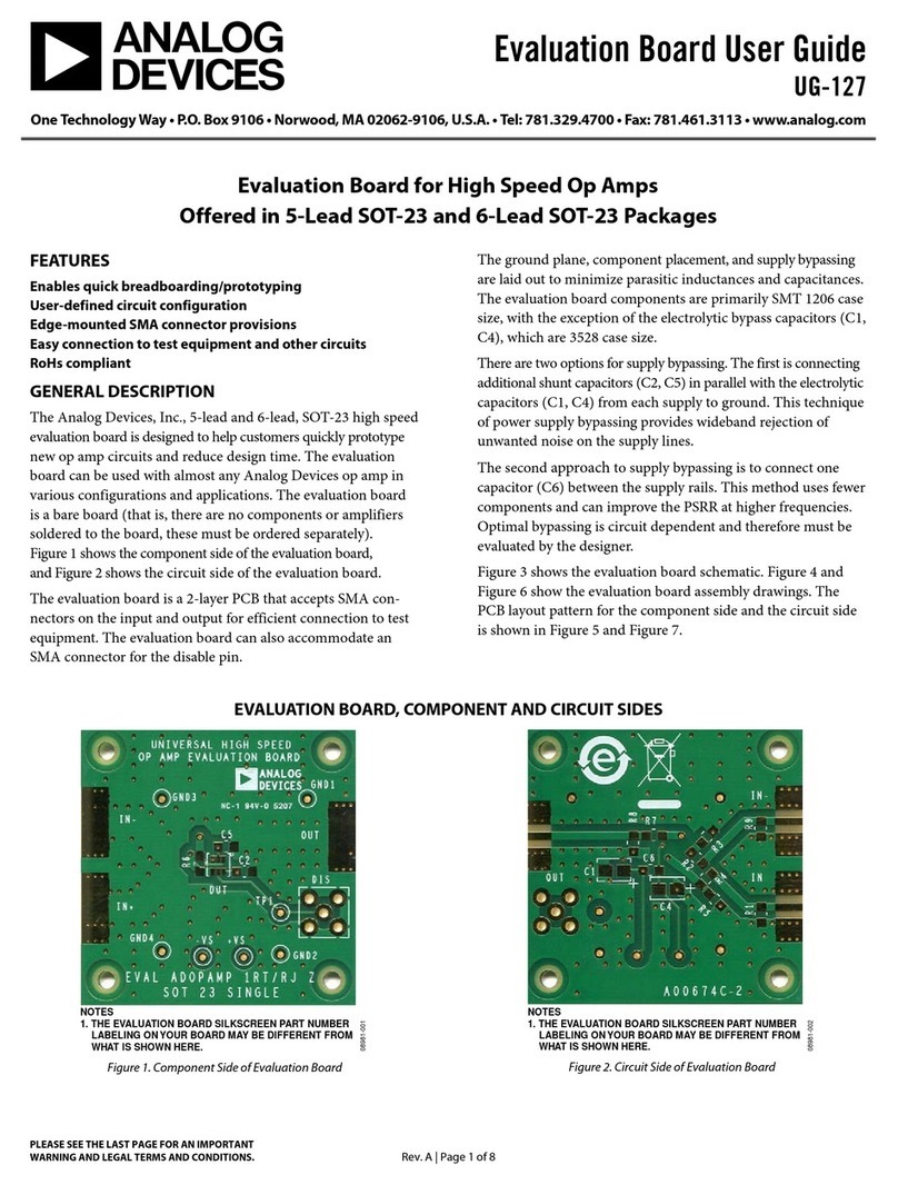
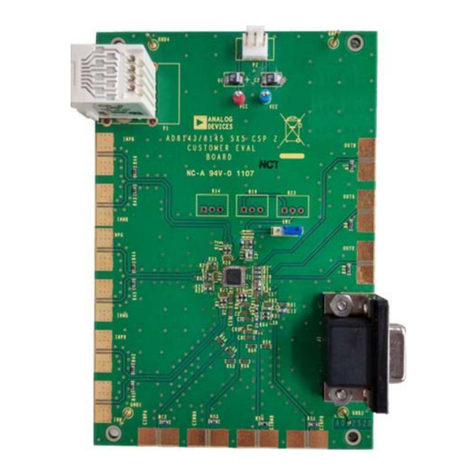
The AD9166-FMC-EBZ evaluation board integrates all
necessary power supply rails, power supply sequencing, and
on-board clock sources. The evaluation board can be powered
by a single 12 V supply. The auxiliary cooling fan is powered
from a 3.3 V rail. Both supplies are provided by the ADS7-V2EBZ.
22324-003
Figure 2. View of the Top of the ADS7-V2EBZ Pattern Generator Board
The evaluation board includes provisions to allow using either
the on-board (internal) clocking or providing reference clocks
from an external source. The user can choose. Generally,
laboratory grade, high frequency clock sources can achieve
best-in-class phase noise performance, which directly translates
to the output of the AD9166. However the on-board clocking
scheme, based on the HMC7044 and ADF4372 ICs, results in
phase noise performance that is comparable or exceeds the
performance of many laboratory grade clock sources, as shown
in Figure 16.
A block diagram of the clock paths on the AD9166-FMC-EBZ
evaluation board is shown in Figure 3.
ON-BOARD CLOCKING
Multiple on-board clock configurations are possible, based on
the HMC7044 and ADF4372. For details on clocking configura-
tions that require external clocking, refer to the External
Clocking section.
The HMC7044 includes two phase-locked loops (PLLs): PLL1
and PLL2. Each loop can operate independently.
Aside from specific configurations where only PLL1 is used, the
HMC7044 is only needed when an active JESD204B link
provides the data samples to the AD9166 through the FMC
connector. In this case, the HMC7044 generates a lane rate/40
(or bit rate/40) clock and a SYSREF± clock to the FPGA on
board the ADS7-V2EBZ, and another SYSREF± clock to the
AD9166, to support a JESD204B link in either Subclass 0 or
Subclass 1. More details are available in the Hardware Setup
section in this user guide, in the JESD204B specifications from
JEDEC, and in the AD9166 data sheet.
PLL1 is a low bandwidth PLL that allows improving the phase
noise (jitter) of an external reference, which typically results in
improved phase noise in the 1/f region of downstream PLLs, a
region that is within the pass band of most PLLs, at offset
frequencies of 1 kHz and below. As a trade-off, the low loop
bandwidth of PLL1 results in a longer lock time if the input
reference frequency is considerably lower than the oscillator
frequency to which the PLL attempts to lock. On the AD9166-
FMC-EBZ evaluation board, PLL1 is used to lock an on-board
122.88 MHz voltage controlled crystal oscillator (VCXO) to an
external reference connected to J61.
The VCXO operates at 122.88 MHz and can be either locked
using PLL1 or left free running by keeping J61 disconnected. It
is generally a good practice to reconfigure the HMC7044 via its
serial peripheral interface (SPI) bus so that its charge pump is
tristated. However, it may not always be necessary because
when PLL1 loses its reference, it automatically enters holdover
and maintains the VCXO control voltage at the last known level.
This means that the input to J61 can be removed while the
AD9166 is running, which may result in small variations in
close in phase noise at the AD9166 output, depending on how
the HMC7044 was configured. It may be good practice to
reprogram the HMC7044 if the reference on J61 is removed.
PLL2 can lock a high frequency, internal voltage controlled
oscillator (VCO) core inside the HMC7044 to the 122.88 MHz
VCXO output. The VCO output is then fed the output fanout
buffer inside the HMC7044 to generate the various clock rates.
See the HMC7044 data sheet for more details.
Instead of PLL2, the user can choose to input a reference clock
to FIN, the external VCO input on the CLKIN1/FIN pin of the
HMC7044, and bypass PLL2 altogether. Using the CLKIN1/FIN
pin is the default clocking scheme on the AD9166-FMC-EBZ
evaluation board, as configured by solder jumpers or 0 Ω
resistors. The input to the CLKIN1/FIN pin is derived from the
ADF4372.
The ADF4372 provides a sample rate clock to the DAC core of
the AD9166. The ADF4372 can also provide a copy of this clock
to the CLKIN1/FIN pin of the HMC7044. Both clocks can be
phase synchronized.
The fractional-N PLL inside the ADF4372 locks an internal
VCO to the VCXO on the AD9166-FMC-EBZ evaluation
board. This is the same VCXO that locks PLL2, when used.
Locking both PLL2 and the ADF4372 to a common reference
allows both to be frequency locked, whether in fractional-N or
integer mode.
By default, the ADF4372 on the AD9166-FMC-EBZ evaluation
board provides both the AD9166 sample rate clock (DAC clock)
and the reference clock to the HMC7044 through the CLKIN1/
FIN pin. PLL2 is not used, and PLL1 can be still used to lock the
VCXO to an external reference from J61.
