UG-1225 EVAL-AD7606BFMCZ User Guide
Rev. A | Page 4 of 15
EVALUATION BOARD HARDWARE
DEVICE DESCRIPTION
The AD7606B is a 16-bit, 8-channel, simultaneous sampling
successive approximation ADC. The device operates from a single
4.75 V to 5.25 V power supply and features throughput rates of
up to 800 kSPS. The device has 5 MΩ input impedance for
direct connection from the user sensor outputs to the ADC.
HARDWARE LINK OPTIONS
Table 2 details the link option functions and the default power
link options. The EVAL-AD7606BFMCZ can be powered by
different sources, as described in the Power Supplies section. By
default, the power supply required for the EVAL-AD7606BFMCZ
comes from the EVAL-SDP-CH1Z (SDP-H1) controller board.
The power supply is regulated by the on-board ADP7118 low
dropout (LDO) regulators, which generates the 5 V supply.
CONNECTORS AND SOCKETS
The connectors and sockets on the EVAL-AD7606BFMCZ are
outlined in Table 1.
Table 1. On-Board Connectors
Connector Function
P12 FPGA mezzanine card (FMC) connector
P4 External power terminal block, 7 V to 9 V dc input
P6, P8 8-pin connectors for input to Channel 1 through
Channel 4
P9, P10 8-pin connectors for input to Channel 5 through
Channel 8
J1 to J4 Analog input Subminiature Version B (SMB)
connectors to Channel 1 through Channel 4
P7, P11 Channel 8 surfboard evaluation headers
P1, P2 General connectors for debugging purposes or to
connect an external controller
The default interface to the EVAL-AD7606BFMCZ is via the
FMC connector, which connects the EVAL-AD7606BFMCZ to
the EVAL-SDP-CH1Z (SDP-H1).
POWER SUPPLIES
Before applying power and signals to the EVAL-AD7606BFMCZ,
ensure that all link positions are set according to the required
operating mode. See Table 2 for the complete list of link
options.
The supply required for the EVAL-AD7606BFMCZ comes
from the EVAL-SDP-CH1Z (SDP-H1) controller board.
Alternatively, the EVAL-AD7606BFMCZ can also be supplied
with a dc power supply connected to the P4 terminal block.
Select the external power supply or the EVAL-SDP-CH1Z
(SDP-H1) supply through JP2. The power supply is then
connected to the on-board ADP7118 5 V linear regulator that
supplies the correct bias to each of the various sections on the
EVAL-AD7606BFMCZ.
CHANNEL INPUT
The J1 to J4 connectors allow users to connect external signals
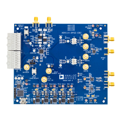
to the ADC channel inputs through the SMB inputs. The EVAL-
AD7606BFMCZ is supplied with the AD7606B mounted (U4,
see Figure 1). The AD7606B is an 8-channel data acquisition
system (DAS) with a simultaneous sampling ADC. External
signals can be applied to the P8 to P10 terminal blocks on the
EVAL-AD7606BFMCZ.
Table 2. Link Options
Link Default Position Function
JP2 A This link selects the power supply source for the evaluation board.
In Position A, the unregulated supply to the on-board LDOs is taken from the EVAL-SDP-CH1Z (SDP-H1) 12 V supply.
In Position B, the unregulated external supply to the on-board LDOs is taken from the P4 terminal block connector.
JP1 A The EVAL-AD7606BFMCZ evaluation software controls the STBY pin. When using the EVAL-AD7606BFMCZ
board in standalone mode without running the EVAL-AD7606BFMCZ evaluation software, this jumper allows
selection of standby mode. In this case, change the R8 and R10 resistors to 0 Ω links.
In Position A, the STBY pin is tied to VDRIVE.
In Position B, the STBY pin is tied to AGND.
