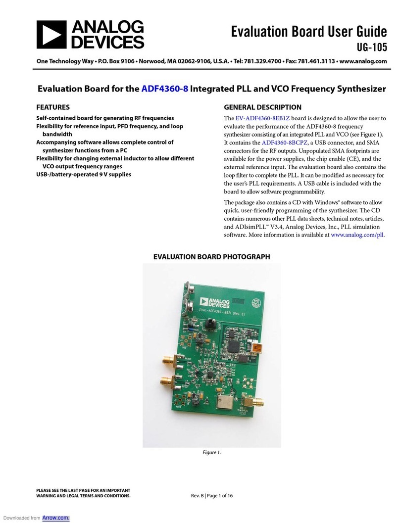
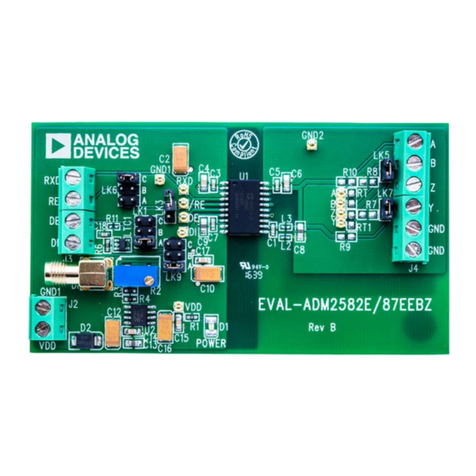
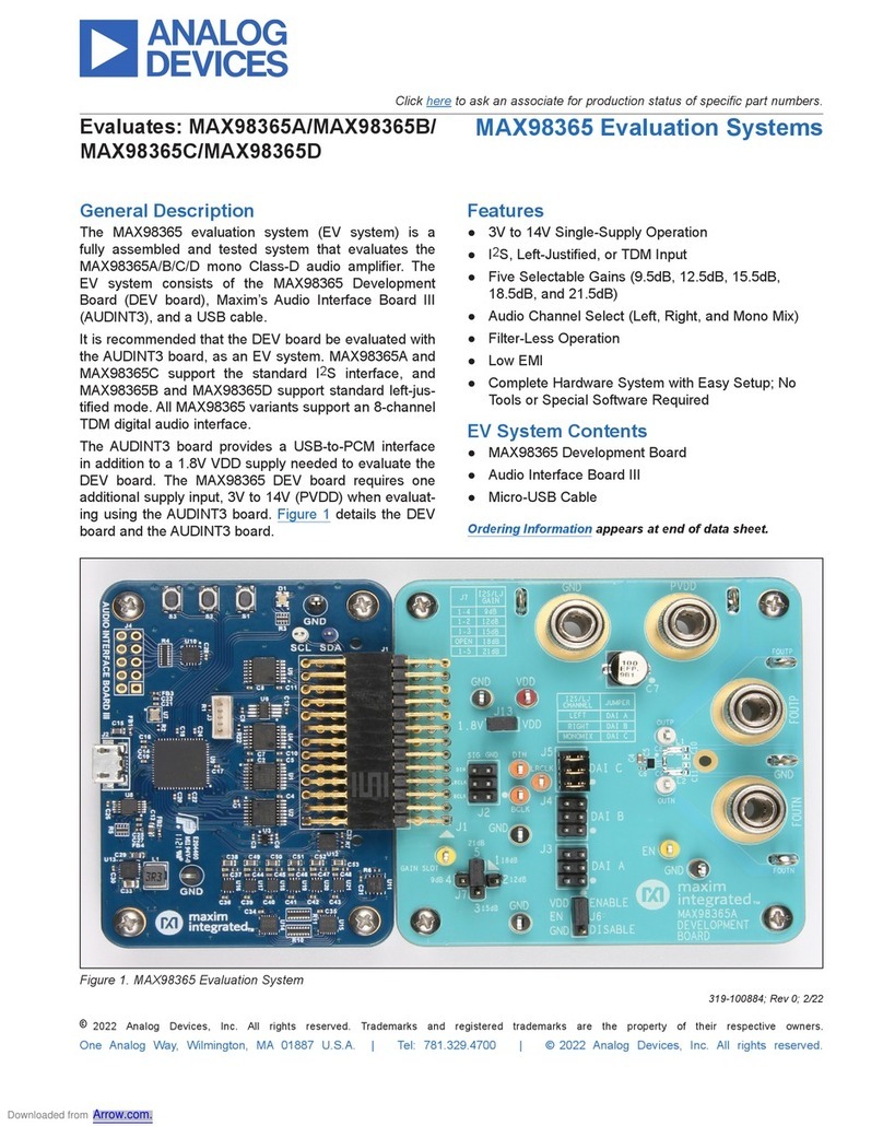
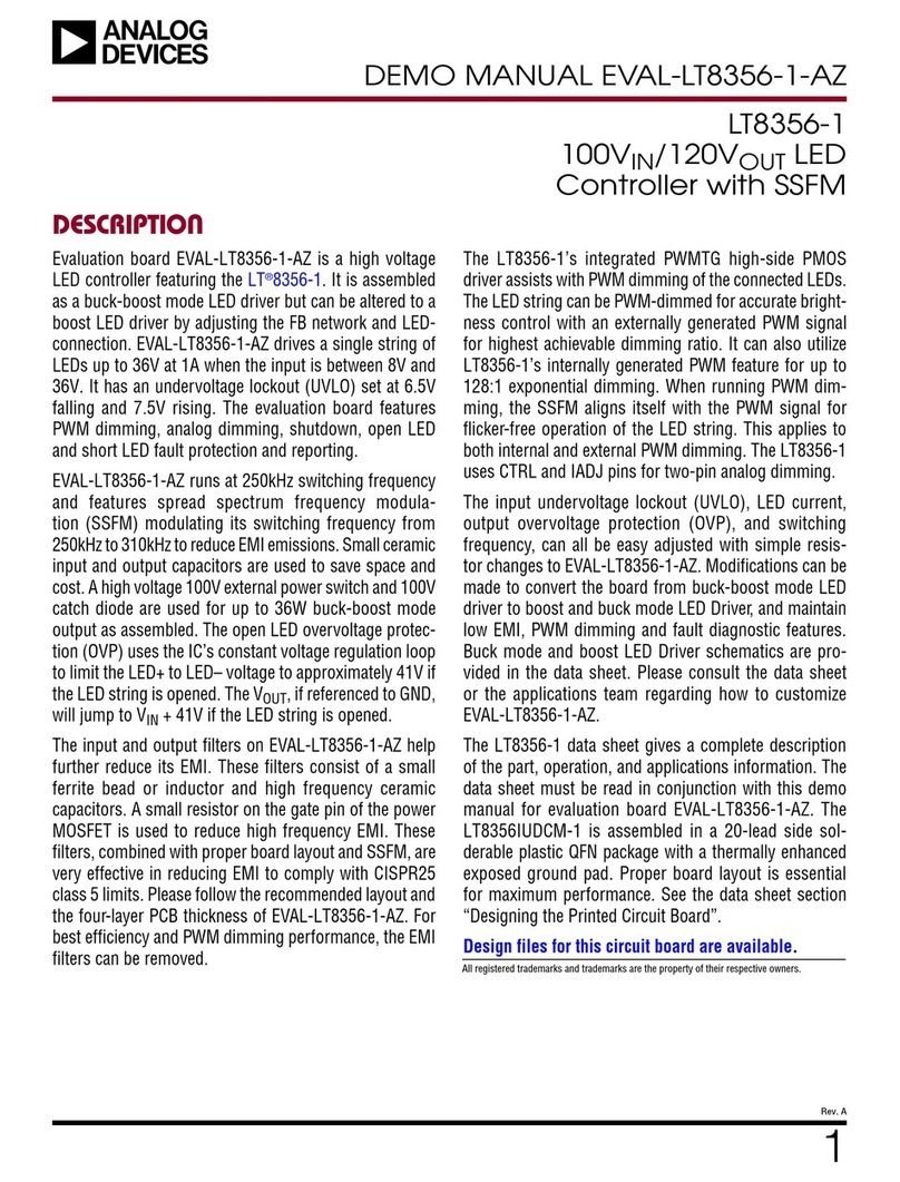
manuals.online logo
Brands
  1. Home
  2. •
  3. Brands
  4. •
  5. Analog Devices
  6. •
  7. Motherboard
  8. •
  9. Analog Devices EVAL-AD7730LEB Specification sheet

Analog Devices EVAL-AD7730LEB Specification sheet

One Technology Way, P.O. Box 9106, Norwood. MA 02062-9106, U.S.A.
Tel: 617/329-4700 Fax: 617/326-8703
a
Evaluation Board for
AD7730L Transducer ADC
EVAL-AD7730LEB
FEATURES
Operates from a Single +5V Supply
On-Board Reference and Digital Buffers
Various Linking Options
Direct Hook-Up to Printer Port of PC
PC Software for Control and Data Analysis
On-Board User Grid Area for Expansion
Interfacing to this board is provided either through a 36-Way
Centronics Connector or through a 9-way D-type connector.
External sockets are provided for the analog inputs, an exter-
nal reference input option and an external master clock
option.
OPERATING THE AD7730L EVALUATION BOARD
POWER SUPPLIES
The evaluation board has four power supply input pins:
AV
DD
, AGND, DV
DD
and DGND. The AD7730L is specified
with an AV
DD
of +5V. Therefore, the AV
DD
voltage supplied
to the board must be +5V. This AV
DD
voltage is also used to
power the AD780 reference. To run the board from a single
+5V supply, simply connect the AV
DD
and DV
DD
inputs
together.
Both AGND and DGND inputs are provided on the board.
AGND connects to the AD7730L AGND pin and also connects
to the GND pin of the AD780. DGND connects to the DGND
pin of the AD7730L and to the GND of the digital chips on the
board. The AGND and DGND planes are connected at the
AD7730L. Therefore, it is recommended not to connect AGND
and DGND elsewhere in the system to avoid ground loop prob-
lems. When using a single supply for both AV
DD
and DV
DD
, only
one ground connection should be made to the board. This
connection should be made to the board's AGND input terminal.
Both supplies are decoupled to their respective ground plane with
10µF tantalum and 0.1µF ceramic disc capacitors.
REV. B
Information furnished by Analog Devices is believed to be accurate and reliable.
However, no responsibility is assumed by Analog Devices for its use, nor for any
infringements of patents or other rights of third parties which may result from
its use. No license is granted by implication or otherwise under any patent or
patent rights of Analog Devices.
INTRODUCTION
This Technical Note describes the evaluation board for the
AD7730L, Transducer ADC. The AD7730L is a complete ana-
log front-end for weigh-scale and pressure measurement applica-
tions. The device accepts low-level signals directly from a trans-
ducer and outputs a serial digital word. The part features two
buffered differential programmable gain analog inputs as well as
a differential reference input. An on-chip 6-bit DAC allows the
removal of TARE voltages. Clock signals for synchronizing ac
excitation of the bridge are also provided. Full data on the
AD7730L is available in the AD7730 data sheet available from
Analog Devices and should be consulted in conjunction with this
Technical Note when using the Evaluation Board.
Included on the evaluation board, along with the AD7730L, are
an AD780, a +2.5 V ultra high precision bandgap reference, a
2.4576MHz crystal and digital buffers to buffer signals to and
from the edge connectors.
FUNCTIONAL BLOCK DIAGRAM
AD7730
ADC
9-WAY D-TYPE CONNECTOR
36-WAY
CENTRONICS
CONNECTOR
AD780
REFERENCE
AIN1(+)
AIN1(-)
AVDD AGND DVDD DGND
AIN2(+)/D1
AIN2(-)/D0
REF IN
BUFFERS
MCLK IN
AVDD
ACX
ACX
EVAL-AD7730LEB
REV. B2
Link Options
There are a number of link options on the evaluation board which should be set for the required operating setup before using
the board. The functions of these link options are described in detail below.
Link No. Function
LK1 This option selects the master clock option for the AD7730L. The master clock source comes from the on-board
crystal or from an external clock source via SKT11. This is a double link and both links must be moved together
for correct operation.
With both links in position A, the external clock option is selected and an externally applied clock to SKT 11 is
routed to the MCLK IN pin of the AD7730L.
With both links in position B, the on-board crystal is selected and provides the master clock for the AD7730L.
LK 2 This link option is used to determine whether the AD7730L is in its normal operating mode or its STANDBY
(power-down) mode.
With this link in position A, the STANDBY input of the AD7730L is connected to a logic high thus configuring
the part for normal operation.
With this link in position B, the STANDBY input of the AD7730L is connected to a logic low and the AD7730L
is placed in its power-down mode where its power dissipation is typically 100µW.
LK3 This link option is used to select the reference source for the AD7730L's REF IN(-) input.
With this link in position A, the REF IN(-) pin of the AD7730L is connected to SKT10. An external voltage
connected to SKT10 can now be used for REF IN(-).
With this link in position B, the REF IN(-) pin of the AD7730L is connected directly to AGND.
LK4 This link controls the polarity of the serial clock.
With this link in position A, the POL pin of the AD7730L is connected to a logic high. With this input high, the
first transition of the serial clock in a data transfer is from a high to a low. This link should be in position A when
operating with the evaluation board software.
With this link in position B, the POL pin of the AD7730L is connected to a logic low. With this input low, the first
transition of the serial clock in a data transfer is from a low to a high.
LK5 This link option is used to select the reference source for the AD7730L's REF IN(+) input.
With this link in position A, the REF IN (+) pin of the AD7730L is connected directly to the output of the on-board
reference, the AD780.
With this link in position B, the REF IN (+) pin of the AD7730L is connected directly to AV
DD
.
With this link in position C, the REF IN(+) pin of the AD7730L is connected to SKT9. An external voltage connected
to SKT9 can now be used for REF IN(+).
LK6 This link is in series with the ACX pin.
With this link in place, SKT5 provides the ACX signal from the AD7730L.
LK7 This link is in series with the ACX pin.
With this link in place, SKT6 provides the ACX signal from the AD7730L.
LK8 This link is in series with the AIN2(+)/D1 pin.
With this link in place, SKT8 is connected directly to the AIN2(+)/D1 pin.
This link may be removed so that an analog input signal at SKT8 can be connected to the component grid for signal
conditioning before being applied to the AIN2(+) input of the AD7730L.
LK9 This link is in series with the AIN2(-)/D0 pin.
With this link in place, SKT7 is connected directly to the AIN2(-)/D0 pin.
This link may be removed so that an analog input signal at SKT7 can be connected to the component grid for signal
conditioning before being applied to the AIN2(-) input of the AD7730L.
LK10 This link is in series with the AIN1(+) analog input.
With this link in place, the analog input on the SKT3 input is connected directly to the AIN1(+) input on the
part.
This link may be removed so that the input signal at SKT3 can be connected to the component grid for
signal conditioning before being applied to the AIN1(+) input of the AD7730L.
EVAL-AD7730LEB
REV. B 3
Setup Conditions
Table I shows the position in which all the links are set when
the evaluation board is sent out.
Table I. Initial Link Positions
Link No. Position Function.
LK1 B Both links in position B to select the
on-board crystal oscillator as the
master clock for the board.
LK2 A Normal Operating Mode.
LK3 B REF IN(-) connected directly to
AGND.
LK4 A POL pin of AD7730L tied high.
LK5 B REF IN(+) connected to the AV
DD
.
LK6 IN ACX connected to SKT5.
LK7 IN ACX connected to SKT6.
LK8 IN SKT8 connected to AIN2(+)/D1.
LK9 IN SKT7 connected to AIN2(-)/D0.
LK10 IN SKT3 connected to AIN1(+).
LK11 IN SKT4 connected to AIN1(-).
Figure 2. SKT1 Pin Configuration
2431 5
6789
Table II. SKT1 Pin Designations
1
1 SCLK Serial Clock. The signal on this pin is buffered
before being applied to the SCLK pin of the
AD7730L.
2RDY Logic Output. This is a buffered version of the
signal on the AD7730L's DRDY pin.
3CS Chip Select. The signal on this pin is buffered
before being applied to the CS pin of the
AD7730L.
4RESET Reset Input. The signal on this pin is buffered
before being applied to the RESET pin of the
AD7730L.
5 DIN Serial Data Input. Data applied to this pin is
buffered before being applied to the AD7730L's
DIN pin.
6 DGND Ground reference point for digital circuitry.
Connects to the DGND plane on the evalua-
tion board.
7 DOUT Serial Data Output. This is a buffered version
of the signal on the AD7730L's DOUT pin.
8DV
DD
Digital Supply Voltage. The DV
DD
voltage for the
evaluation board can be supplied via this pin
provided no voltage is applied to the main DV
DD
terminal.
9SYNC Logic Input. The signal on this pin is buffered
before being applied to the SYNC pin of the
AD7730L.
NOTE
1
An explanation of the AD7730L functions mentioned here is given in Table
III as part of the SKT2 pin designations description.
Link Options (Cont'd)
Link No. Function
LK11 This link is in series with the AIN1(-) analog input.
With this link in place, the analog input on the SKT4 input is connected directly to the AIN1(-) input on the
part.
This link may be removed so that the input signal at SKT4 can be connected to the component grid for
signal conditioning before being applied to the AIN1(-) input of the AD7730L.
EVALUATION BOARD INTERFACING
Interfacing to the evaluation board is either via a 9-way D-
Type connector, SKT1, or a 36-way Centronics connector,
SKT2. The pinout for the SKT1 connector is given in Figure
1 and its corresponding pin designations are given in Table II.
The pinout for this SKT2 connector is shown in Figure 2 and
its pin designations are given in Table III. The evaluation
board should be powered up before a cable is connected to
either of the connectors.
SKT2 is used to connect the evaluation board to the printer
port (parallel port) of a PC. Connection between the two is
direct via a standard parallel printer port cable. SKT1 is used
to connect the evaluation board to any other system.
EVAL-AD7730LEB
REV. B4
118
1936
Figure 3. SKT2 Pin Configuration
Table III. SKT2 Pin Designations
1 NC No Connect. This pin is not connected on the evaluation board.
2 DIN Serial Data Input. Data applied to this pin is buffered before being applied to the AD7730L's DIN pin. The
serial data applied to the DIN pin is written to the input shift register on the part. Data from this input shift
register is transferred to one of the on-chip registers depending on the register selection bits of the
Communications Register.
3RESET Reset Input. The signal on this pin is buffered before being applied to the RESET pin of the AD7730L. RESET
is an active low input which resets the control logic, interface logic, calibration coefficients, digital filter and
all on-chip registers to power-on status.
4CS Chip Select. The signal on this pin is buffered before being applied to the CS pin of the AD7730L. CS is an
active low logic input used to select the AD7730L. With this input hard-wired low, the AD7730L operates in
its three-wire interface mode with SCLK, DIN and DOUT used to interface to the device. CS can be used to
select the device in systems with more than one device on the serial bus or as a frame synchronisation signal
in communicating with the AD7730L.
5 SCLK Serial Clock. The signal on this pin is buffered before being applied to the SCLK pin of the AD7730L. An
external serial clock is applied to this input to access serial data from the AD7730L. This serial clock can be
a continuous clock with all data transmitted in a continuous train of pulses. Alternatively, it can be a non-
continuous clock with the information being transmitted to the AD7730L in smaller batches of data.
6SYNC Logic Input. The signal on this pin is buffered before being applied to the SYNC pin of the AD7730L. The
SYNC input allows for synchronisation of the digital filters and analog modulators across a number of
AD7730Ls. While
SYNC is low, the nodes of the digital filter, the filter control logic, and the calibration control
logic are reset and the analog modulator is also held in its reset state.
7-8 NC No Connect. These pins are not connected on the evaluation board.
9DV
DD
Digital Supply Voltage. This provides the supply voltage for IC4, the buffer chip which buffers the output
signals from the AD7730L before they are applied to SKT2.
10 RDY Logic output. This is a buffered version of the signal on the AD7730L's RDY pin. RDY is used as a status output
in both conversion and calibration mode. In conversion mode, a logic low on the RDY output indicates that
a new output word is available from the AD7730L data register. The RDY pin will return high upon completion
of a read operation of a full output word. If no data read has taken place after an output update, the RDY line
will return high prior to the next output update, remain high while the update is taking place and return low
again. This gives an indication of when a read operation should not be initiated to avoid reading from the data
register as it is being updated. In calibration mode, RDY goes high when calibration is initiated and returns
low to indicate that calibration is complete.
11-12 NC No Connect. These pins are not connected on the evaluation board.
13 DOUT Serial Data Output. This is a buffered version of the signal on the AD7730L's DOUT pin. Serial data from the
output shift register on the part is clocked out on this pin. This output shift register contains information from
one of the nine on-chip registers depending on the register selection bits of the Communications Register.
14-18 NC No Connect. These pins are not connected on the evaluation board.
19-30 DGND Ground reference point for digital circuitry. Connects to the DGND plane on the evaluation board.
31-36 NC No Connect. These pins are not connected on the evaluation board.
EVAL-AD7730LEB
REV. B 5
SOCKETS
There are eleven sockets on the AD7730L evaluation board. The
function of these sockets is outlined in Table IV.
Table IV. Socket Functions
Socket Function
SKT1 9-Way D-Type Connector which can be used for
digital interfacing to the evaluation board.
SKT2 36-Way Centronics Connector which can be used
for digital interfacing to the evaluation board.
This connector should be used when connecting
the board to the parallel printer port of the PC to
use the evaluation software.
SKT3 Sub-Minature BNC (SMB) Connector. The ana-
log input signal for the AIN1(+) input of the AD7730L
is applied to this socket.
SKT4 Sub-Minature BNC (SMB) Connector. The analog
input signal for the AIN1(-) input of the AD7730L is
applied to this socket.
SKT5 Sub-Minature BNC (SMB) Connector. This socket
provides the ACX ouput from the AD7730L.
SKT6 Sub-Minature BNC (SMB) Connector. This socket
provides the ACX ouput from the AD7730L.
SKT7 Sub-Minature BNC (SMB) Connector. Connects to
the AIN2(-)/D0 pin of the AD7730L.
SKT8 Sub-Minature BNC (SMB) Connector. Connects to
the AIN2(+)/D1 pin of the AD7730L.
SKT9 Sub-Minature BNC (SMB) Connector. The refer-
ence voltage for the REF IN(+) input of the AD7730L
is applied to this socket when the board is configured
for an externally-applied reference voltage.
SKT10 Sub-Minature BNC (SMB) Connector. The refer-
ence voltage for the REF IN(-) input of the AD7730L
is applied to this socket when the board is configured
for an externally-applied reference voltage.
SKT11 Sub-Minature BNC (SMB) Connector. The master
clock signal for the MCLK IN input of the AD7730L
is applied to this socket when the board is configured
for an externally-applied master clock..
RUNNING THE AD7730L INTERFACE SOFTWARE
Included in the evaluation board package is a PC-compatible
disk which contains software for controlling and evaluating
the performance of the AD7730L using the printer port of a PC.
There are a total of thirteen files on the distribution disk.
To use the software, the user must have an IBM-compatible PC
and Windows 3.1 must be installed. Start Windows and, using
either the RUN command or the File Manager, start the program
called SETUP.EXE on the distribution disk. This automatically
installs the application and sets up a window called ANALOG
DEVICES. The application ICON is found here. To start the
application, double click on the ICON.
When the program starts, the user is asked to select a printer port.
The correct selection depends on what type of computer is being
used (Desktop, Laptop etc). LPT1 works for most machines.
When using a Compaq laptop, select PRN. A different port can
be selected at any time from the MAIN MENU.
After selecting the printer port, the program displays the Main
Menu as outlined in Figure 4. There are a number of buttons
on the Main Menu which select a variety of different func-
tions. These are described below.
Program AD7730L
Pressing this button calls up a second screen which displays
the contents of the Status Register and provides another set of
buttons allowing the user to program the on-chip registers.
Figure 5 shows the "Program AD7730L" screen. Pressing any of
the buttons on this screen pulls up a further screen allowing all
functions in a register to be programmed. Figure 6 gives an
example of one of these screens (the screen for programming
the Mode Register).
Read Data
The Read Data button allows the user access to the "read
data" screen. On this screen, the user can choose whether the
reading of data is for noise analysis or simply for display. It also
allows the user to choose how many outputs of the AD7730L
should be read for the noise analysis routines.
Noise Analysis
The Noise Analysis button gives the user access to the "noise
analysis" screen. Here the user can look at the results of a data
read in terms of rms code distribution, code spread etc. The
user also has the facility to plot the data versus time and plot
histogram results.
Reset AD7730L
Pressing this button allows the user access to the reset menu
where either a hardware reset (via the RESET pin) or an
software/interface reset (via writing 32 1's) can be selected.
The user also has a hardware reset button on the board.
EVAL-AD7730LEB
REV. B6
Fast Step Demo
This button activates the Fast Step demonstration screen. This
screen allows the user to view and compare the FastStep
response of the AD7730L against it's normal response.
Read from File
Pressing this button allows the user to read data from a file for
noise analysis. The data to be read can either be in decimal or
hexadecimal format.
Write to File
This button allows the user to store of output data from the
AD7730L to a file in either decimal or hexadecimal format. This
data can be used in other programs or can subsequently be read
back to the AD7730L software.
Select Printer Port
This button allows the user to select the printer port to which
the AD7730L evaluation is connected.
About
This provides details of the software revision.
Figure 4. Main Screen
EVAL-AD7730LEB
REV. B 7
Figure 6. Mode Register Screen
Figure 5. Program Screen
EVAL-AD7730LEB
REV. B8
Figure 7. AD7730L Evaluation Board Circuit Diagram
EVAL-AD7730LEB
REV. B 9
COMPONENT LISTING AND MANUFACTURERS
Intergrated Circuits
Component Location Vendor
AD7730LR IC1 Analog Devices
AD780AN IC2 Analog Devices
74HC4050N IC3 Philips
74C08N IC4 Texas Instruments
74HC244N IC5 Texas Instruments
HP 5082-2810 D1 D2 Hewlett Packard
Capacitors
Component Location Vendor
10µF ± 20% Tantalum (16 V) C1 C3 C5 C9 AVX- Kyocera, Mftrs No TAG106MO16
0.1µF Ceramic(X7R ±20%) C2 C4 C6 C7 C8 C10 C15 C16 Philips, Mftrs No. CW20C 104M
Open Circuit C11 C12 C13 C14 ----------
33pF ±2% Ceramic C16 C17 Philips, Mftrs No. 683 34339
Resistors
Component Location Vendor
Short Circuits R1 R2 R3 R4 ----------
3kΩ±5% 0.25W R5 Bourns 3kΩ±5% 0.25W
10kΩ±5% 0.25W R6 R7 R8 Bourns
1MΩ±5% 0.25W R9 Bourns
Link Options, Switches & Sockets
Component Location Vendor
Pin Headers Lk1 (4x2 way) Harwin, Mftrs No. M20-9993606
Lk2 Lk3 Lk4 ( 2x2 way)
Lk5 (3x2 way)
Lk6 Lk7 Lk8 Lk9 Lk10 Lk11 (1x2 way)
Shorting Plugs Pin Headers (12 required) Harwin, Mftrs No. M7571-05
Push Button Switch SW1 Omron, Mftrs No. B3F1000
Miniature BNC Connectors SKT3 - SKT11 ITT Sealectro, Mftrs No. B51-051-0000220
9-Way D-Type Connector SKT1 McMurd0, Mftrs No. SDE9PNTD
36 Way Centronics Connector SKT 2 Fujitsu, Mftrs No. FCN785J036G0
24-Pin IC Socket IC1 Harwin, Mftrs No. D28xx-01 (xx = No. Pins)
16-Pin IC Socket IC3
14- Pin IC Socket IC4
20-Pin IC Socket IC5
Wire Wrap Pins DGND AGND AVDD DVDD Bicc Vero, Mftrs No. 663472C
Crystal Oscillator
Component Identification Location Vendor
2.4576 MHz Oscillator Xtal 1 IQD, Mftrs No. A116C
EVAL-AD7730LEB
REV. B10
Figure 8. Component Layout diagram
EVAL-AD7730LEB
REV. B 11
Figure 9. Component Side Artwork Diagram
EVAL-AD7730LEB
REV. B12
Figure 10. Solder Side Artwork Diagram

Other Analog Devices Motherboard manuals

Analog Devices UG-474 User manual

Analog Devices

Analog Devices UG-474 User manual

Analog Devices AD8556-EVALZ User manual

Analog Devices

Analog Devices AD8556-EVALZ User manual

Analog Devices EVAL-AD5142DBZ User manual

Analog Devices

Analog Devices EVAL-AD5142DBZ User manual

Analog Devices EVAL-AD7173-8SDZ User manual

Analog Devices

Analog Devices EVAL-AD7173-8SDZ User manual

Analog Devices EVAL-SSM2317-MINI User manual

Analog Devices

Analog Devices EVAL-SSM2317-MINI User manual

Analog Devices EVAL-ADPD2140Z User manual

Analog Devices

Analog Devices EVAL-ADPD2140Z User manual

Analog Devices AD9516 User manual

Analog Devices

Analog Devices AD9516 User manual

Analog Devices ADRF5515A-EVALZ User manual

Analog Devices

Analog Devices ADRF5515A-EVALZ User manual

Analog Devices EVAL-ADP1653EB User manual

Analog Devices

Analog Devices EVAL-ADP1653EB User manual

Analog Devices MAX30001G User manual

Analog Devices

Analog Devices MAX30001G User manual

Analog Devices AD9522 Series User manual

Analog Devices

Analog Devices AD9522 Series User manual

Analog Devices ADZS-21569-EZKIT User manual

Analog Devices

Analog Devices ADZS-21569-EZKIT User manual

Analog Devices AD9204-65EBZ User manual

Analog Devices

Analog Devices AD9204-65EBZ User manual

Analog Devices ADSP-2181 User manual

Analog Devices

Analog Devices ADSP-2181 User manual

Analog Devices MAX77859 User manual

Analog Devices

Analog Devices MAX77859 User manual

Analog Devices EVAL-ADGS5412SDZ User manual

Analog Devices

Analog Devices EVAL-ADGS5412SDZ User manual

Analog Devices Linear Technology DC2622A Quick setup guide

Analog Devices

Analog Devices Linear Technology DC2622A Quick setup guide

Analog Devices EVAL-ADF4602EB1Z Instruction manual

Analog Devices

Analog Devices EVAL-ADF4602EB1Z Instruction manual

Analog Devices AD5162 User manual

Analog Devices

Analog Devices AD5162 User manual

Analog Devices AD7273 User manual

Analog Devices

Analog Devices AD7273 User manual

Analog Devices EVAL-ADF4108EBZ1 User manual

Analog Devices

Analog Devices EVAL-ADF4108EBZ1 User manual

Analog Devices EVAL-AD5693RSDZ User manual

Analog Devices

Analog Devices EVAL-AD5693RSDZ User manual

Analog Devices EVAL-ADAS3022EDZ User manual

Analog Devices

Analog Devices EVAL-ADAS3022EDZ User manual

Analog Devices EVAL-ADXRS290Z-M User manual

Analog Devices

Analog Devices EVAL-ADXRS290Z-M User manual

Popular Motherboard manuals by other brands

Asus P4PE-X TE user guide

Asus

Asus P4PE-X TE user guide

NXP Semiconductors Freescale KIT33905 user guide

NXP Semiconductors

NXP Semiconductors Freescale KIT33905 user guide

Microchip Technology SAM D21 user guide

Microchip Technology

Microchip Technology SAM D21 user guide

IEI Technology IMBA-C2160 user manual

IEI Technology

IEI Technology IMBA-C2160 user manual

TYAN Thunder K8S Pro manual

TYAN

TYAN Thunder K8S Pro manual

WanSen NEAT-471 user guide

WanSen

WanSen NEAT-471 user guide

Biostar P4 TGS Engineering validation test report

Biostar

Biostar P4 TGS Engineering validation test report

Asus A7N8X-LA (Focus) user guide

Asus

Asus A7N8X-LA (Focus) user guide

EPC 611 How to get started

EPC

EPC 611 How to get started

ASROCK B250M-HDV user guide

ASROCK

ASROCK B250M-HDV user guide

Texas Instruments BQ79606EVM user guide

Texas Instruments

Texas Instruments BQ79606EVM user guide

Texas Instruments CC2545EMK quick start guide

Texas Instruments

Texas Instruments CC2545EMK quick start guide

ST AN3959 Application note

ST

ST AN3959 Application note

ECS A785GM-AD3 manual

ECS

ECS A785GM-AD3 manual

Intel DH67VR Product guide

Intel

Intel DH67VR Product guide

DFI AZ30-EC user manual

DFI

DFI AZ30-EC user manual

Asus M4A78 PRO - Motherboard - ATX user manual

Asus

Asus M4A78 PRO - Motherboard - ATX user manual

Gigabyte GA-Z77P-D3 user manual

Gigabyte

Gigabyte GA-Z77P-D3 user manual

manuals.online logo
manuals.online logoBrands
  • About & Mission
  • Contact us
  • Privacy Policy
  • Terms and Conditions

Copyright 2025 Manuals.Online. All Rights Reserved.