manuals.online logo
Brands
  1. Home
  2. •
  3. Brands
  4. •
  5. Analog Devices
  6. •
  7. Motherboard
  8. •
  9. Analog Devices EVAL-AD9888EB User manual

Analog Devices EVAL-AD9888EB User manual

AD9888 Evaluation Board
EVAL-AD9888EB
Rev. 0
Information furnished by Analog Devices is believed to be accurate and reliable.
However, no responsibility is assumed by Analog Devices for its use, nor for any
infringements of patents or other rights of third parties that may result from its use.
Specifications subject to change without notice. No license is granted by implication
or otherwise under any patent or patent rights of Analog Devices. Trademarks and
registered trademarks are the property of their respective companies.
One TechnologyWay, P.O.Box 9106,Norwood, MA 02062-9106, U.S.A.
Tel:781.329.4700www.analog.com
Fax: 781.326.8703 © 2003 Analog Devices, Inc. All rights reserved.
GENERAL DESCRIPTION
The EVAL-AD9888EB can be used both to demonstrate the
performance of the AD9888 and to serve as an implementation
example for design and layout. To aid in real-world evaluation,
the EVAL-AD9888EB was designed to be connected as easily as
possible into another PCB, such as a graphics controller board.
REQUIREMENTS
The EVAL-AD9888EB requires a 5 V power supply, graphics
signals (through either of the 15-pin VGA connectors), and a
means to program the internal chip registers. PC compatible
hardware and software are provided for programming the
internal chip registers.
TYPICAL CONFIGURATION
In most cases, this evaluation board will be used to digitize
analog RGB graphics signals and pass the data on to another
board. To do this, connect the graphics signals to either of the
15-pin VGA connectors, supply 5 V to the board, and program
the internal serial register. Supplying power and programming
the chip are described later in this data sheet. The digitized data,
generated clock signals, and control signals are passed off the
board through the right-side Connector J3.
POWER
The EVAL-AD9888EB contains three 3.3 V voltage regulators,
which supply power to the AD9888’s three power supplies (refer
to the AD9888 Data Sheet). Best performance can be obtained
from the AD9888 when the analog supply (VD) and the PLL
supply (PVD) have their own regulators separate from the
primary 3.3 V supply (VDD). The three regulators work
nominally when supplied with 5 V, but will work with a range of
voltages. Power is applied to the board through the right-side
connector (Pins 1, 2, 41, and 42 of J3). Typically, power is
supplied from another board, as is the case when using the
UXGA panel driver board.
SYNC SELECTION FOR J3 BOARD INTERFACE
The EVAL-AD9883EB provides for raw Hsync and Vsync
selection to connector J3 via the 3-pin jumpers labeled HS_SEL
and VS_SEL. If the raw Hsync and Vsync are to be used by the
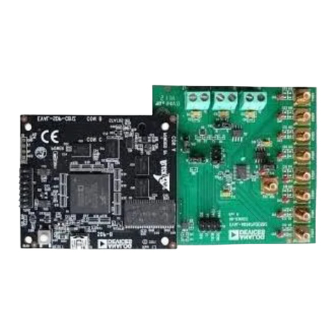
Figure 1. The AD9888 Evaluation Board
connected interface board (whether it be a panel driver board
or other type of board), these jumpers should be placed
appropriately depending on which video input is selected. If
input 0 is selected, the jumpers should be placed in the 0
position (as marked on the PCB); If 1 is selected, the jumpers
should be placed in the 1 position.
CHIP REGISTER NAMING CONVENTION
There are several references in this data sheet to specific control
registers in the AD9888. The convention used in this data sheet
is to specify the register number in hex, followed by an “h” and
by the bit number within the register. For example, [12h7]
means Register 12, Bit 7.
PROGRAMMING THE INTERNAL CHIP REGISTERS
Hardware and software are provided for programming the
AD9888 internal registers. The hardware consists of a standard
printer cable and a receiver chip located on the panel driver
board. The programming signals come onto the EVAL-
AD9888EB through Pins 38 and 39 on Connector J3. The
software is included on the installation CD-ROM and is
described in the Setup Software section.
EVAL-AD9888EB
Rev. 0 | Page 2 of 4
Figure 2. AD9888 Register Setup Screen
SETUP SOFTWARE the Load button at the top of the window in order to update the
registers. If Load Registers on Change is checked, the
appropriate register is updated as soon as any change is made in
the window. There are three tabs within this control window
that enable the selection of register groups to be displayed. The
selections are: 00–0F, 10–14, or 15. Click the appropriate tab to
view and/or control the desired register.
The Display Electronics Product Line (DEPL) evaluation soft-
ware is a Visual Basic® program that requires Windows® 95 or
newer. The software comes on a self-installing CD-ROM that is
included with the evaluation board. When installing the soft-
ware, always use the most recent Windows files (e.g., .dll or
.ocx) if prompted by the install software (these files may already
be on your system). The AD9888 register setup screen shown in
Figure 2 is displayed at program execution after installation.
The DEPL evaluation software can be used to control any DEPL
AD988x device. It also includes the display interface board
configuration software and a PLL divisor calculator.
PLL Settings
The PLL settings are contained in Registers 01h to 04h. The PLL
Divisor setting (12 bits) can be set bit-by-bit (the value toggles
when clicking on the bit), by setting a value (in decimal) for
Registers 01h and 02h, by setting the 12-bit value (in decimal),
or by moving the control bar right or left to increase or decrease
the value. When changing the value using one of these methods,
the change is reflected in the other three. Both registers are
written to at the same time to avoid discontinuities in the 12-bit
setting. The VCO Range and Charge Pump settings in Register
03h can be set bit-by-bit, by register, or by pull-down menu
selection. The 5-bit Phase Adjust in Register 04h can be altered
in the same manner as the PLL Divisor.
AD9888 SOFTWARE CONTROL
To select the AD9888 as the DEPL evaluation software’s target
device, select AD9888 from the Device pull-down menu. From
the AD9888 register setup screen (shown in Figure 2), the user
can control every bit within the AD9888. A detailed, bit-by-bit
functional description is provided in the AD9888 Data Sheet.
Unless Load Register On Change is clicked, the user must click
EVAL-AD9888EB
Clamp and Hsync Out Settings
Clamp Placement, Clamp Duration, and Hsync Out Width
controls are contained in Registers 05h to 07h and can be
changed bit-by-bit, by setting a value for the registers (decimal
value), or by moving the control bar right or left to increase or
decrease the value. When changing the value using one of these
methods, the change is reflected in the other two. Again, unless
the Load Register On Change box is checked, these value
changes are not loaded into the AD9888 until the Load button is
clicked. Note that Clamp Placement values of 1, 2, 4, 8, 16, 32,
64, and 128 are not supported.
Gain and Offset Settings
Gain for the red, green, and blue video channels is controlled via
all eight bits of Registers 08h to 0Ah and can be changed bit-by-
bit, by setting a value for the registers (decimal value), or by
moving the control bar right or left to increase or decrease the
value. The 7-bit offset control for the red, green, and blue
channels is contained in Registers 0Bh to 0Dh. These can be set
in the same manner as gain, with the additional option of
setting the 7-bit decimal value. Note that using the gain and
offset control bars will change all three channels by the same
amount, regardless of their setting. For example, if, in order to
achieve color balance, the offset settings are 60, 70, and 80 for R,
G, and B, respectively, the minimum settings are 0, 10, and 20.
The maximum offset settings would then be 107, 117, and 127.
Note that for the purpose of having the cleanest placement and
routing of the analog inputs, the EVAL-AD9888EB’s red and
blue inputs are reversed. In other words, the red analog data is
routed through the AD9888’s blue channel and vice versa.
Therefore, if a blue offset and gain adjustment is desired, the
registers for the red channel should be modified.
Sync Control
Register 0Eh contains bits for controlling input and output
Hsync and Vsync signals. The user can toggle each bit by
clicking on it. The resulting state of a bit is reflected in the box
to the right of that bit. Refer to the AD9888 Data Sheet for a
functional description of these bits.
Clamp, Coast, and Power Management
Register 0Fh contains bits for controlling the Clamp and Coast
functions, as well as Power Management functions. The user
can toggle each bit by clicking on it. The resulting state of the
bits is reflected in the box to the right of each bit. Refer to the
AD9888 Data Sheet for a functional description of these bits.
SOG and Clamp Control
Register 10h contains bits for controlling the SOG threshold
and Clamp selection functions. Register 11h contains bits for
adjusting the Sync separator threshold. The 5-bit (Reg 10h7:3)
SOG Threshold can be modified bit-by-bit, by changing the
5-bit (decimal) value, or by sliding the control bar. The user can
toggle each Clamp selection bit by clicking on it. The resulting
state of the bits is reflected in the box to the right of each bit.
The Sync separator threshold can be changed bit-by-bit, by
setting a value for the register (decimal value), or by moving the
control bar right or left to increase or decrease the value. See the
AD9888 Data Sheet for a functional description of these bits.
Pre-Coast and Post-Coast
Registers 12h and 13h contain the bits for controlling Pre-Coast
and Post-Coast. The 8-bit Pre-Coast and 8-bit Post-Coast can
be modified bit-by-bit, by changing the 8-bit (decimal) value, or
by sliding the control bar. The resolution of this adjustment,
which applies to the AD9888’s internal Coast function and does
not alter external Coast signals, is in Hsync periods. See the
AD9888 Data Sheet for a functional description of these bits.
Sync and Coast Status (Read-Only)
Register 14h is a read-only register that provides status for
Hsync, Vsync, SOG, and Coast polarity. Performing a read (by
clicking the Read button) allows the user to see the status of
each of these bits. The status is also reflected in the text to the
right of each of these bits. See the AD9888 Data Sheet for a
functional description of these bits.
Input/Output Modes
Register 15h contains bits for controlling input and output
modes. These include output formatting, input select, and
bandwidth control. The user can toggle each bit by clicking on
it. The resulting state of the bits is reflected in the box to the
right of each bit. See the AD9888 Data Sheet for a functional
description of these bits.
OTHER SOFTWARE FEATURES
PLL Divider Calculator
The AD9888 register setup software includes a calculator that
computes the PLLDIV setting. Simply click the Calculator
button at the bottom left side of the window and enter the pixel
clock and Hsync frequencies.
SCHEMATICS AND LAYOUT
The schematics and layout for this board are included in
separate files. They can be found on the CD-ROM.
CONTACT INFORMATION
If you have questions or would like more information, email us
directly at flatpanel_apps@analog.com, visit our website at
http://www.analog.com/flatpanel, or call the Analog Devices
help line at 1-800-AnalogD (1-800-262-5643).
Rev. 0 | Page 3 of 4
EVAL-AD9888EB
Rev. 0 | Page 4 of 4
Table 1. Sample Settings for the EVAL-AD9888EB
PLL Timing Chart
Horizontal Sync
Mode Resolution
Nominal Frequency
(kHz) Polarity
PLL Divider1
N + 1
Nominal Pixel
Clock (MHz)
VCO
Range2
Charge Pump
Current2
VGA 640 × 480 @ 60 Hz 31.469 N 800 25.175 00 010
640 × 480 @ 72 Hz 37.861 N 832 31.500 00 100
640 × 480 @ 75 Hz 37.500 N 840 31.500 00 100
640 × 480 @ 85 Hz 43.269 N 832 36.000 00 100
SVGA 800 × 600 @ 56 Hz 35.156 N/P 1024 36.000 00 100
800 × 600 @ 60 Hz 37.879 P 1056 40.000 00 101
800 × 600 @ 72 Hz 48.077 P 1040 50.000 01 011
800 × 600 @ 75 Hz 46.875 P 1056 49.500 01 011
800 × 600 @ 85 Hz 53.674 P 1048 56.250 01 011
XGA 1024 × 768 @ 60 Hz 48.363 N 1344 65.000 01 100
1024 × 768 @ 70 Hz 56.476 N 1328 75.000 01 100
1024 × 768 @ 75 Hz 60.023 P 1312 78.750 01 101
1024 × 768 @ 80 Hz 64.000 P 1336 85.500 10 011
1024 × 768 @ 85 Hz 68.677 P 1376 94.50 10 011
SXGA 1280 × 1024 @ 60 Hz 60.020 P 1688 108.000 10 011
1280 × 1024 @ 75 Hz 80.000 P 1688 135.000 10 100
1280 × 1024 @ 85 Hz 91.100 P 1730 157.500 11 100
UXGA 1280 × 1024 @ 60 Hz 75.000 P 2160 162.000 11 100
1280 × 1024 @ 65 Hz 81.300 P 2160 175.500 11 100
1280 × 1024 @ 70 Hz 87.500 P 2160 189.000 11 101
1280 × 1024 @ 75 Hz 93.800 P 2160 202.500 11 101
1PLL divisor to the chip should be an odd integer; Chip divide ratio = Input N + offset of 1.
2The VCO range and charge pump current settings are preliminary and may need slight adjustments.
ESD CAUTION
ESD (electrostatic discharge) sensitive device. Electrostatic charges as high as 4000 V readily accumulate on the
human body and test equipment and can discharge without detection. Although this product features
proprietary ESD protection circuitry, permanent damage may occur on devices subjected to high energy
electrostatic discharges. Therefore, proper ESD precautions are recommended to avoid performance
degradation or loss of functionality.
ORDERING GUIDE
Model Package Description
AD9888/PCB Evaluation Board
© 2003 Analog Devices, Inc. All rights reserved. Trademarks and
registered trademarks are the property of their respective companies.
C04329–0–7/03(0)

Other Analog Devices Motherboard manuals

Analog Devices EV-ADE9153ASHIELDZ User manual

Analog Devices

Analog Devices EV-ADE9153ASHIELDZ User manual

Analog Devices EVAL-AD2437A1MZ User manual

Analog Devices

Analog Devices EVAL-AD2437A1MZ User manual

Analog Devices UG-182 User manual

Analog Devices

Analog Devices UG-182 User manual

Analog Devices ADP151 User manual

Analog Devices

Analog Devices ADP151 User manual

Analog Devices EVAL-AD5592RSDZ User manual

Analog Devices

Analog Devices EVAL-AD5592RSDZ User manual

Analog Devices DC2881A-A User manual

Analog Devices

Analog Devices DC2881A-A User manual

Analog Devices EVAL-ADAQ7768-1 User manual

Analog Devices

Analog Devices EVAL-ADAQ7768-1 User manual

Analog Devices Linear DC2515 Quick setup guide

Analog Devices

Analog Devices Linear DC2515 Quick setup guide

Analog Devices EVAL-AD5676SDZ User manual

Analog Devices

Analog Devices EVAL-AD5676SDZ User manual

Analog Devices EVAL-ADP5020 User manual

Analog Devices

Analog Devices EVAL-ADP5020 User manual

Analog Devices EVAL-AD5341DBZ User manual

Analog Devices

Analog Devices EVAL-AD5341DBZ User manual

Analog Devices EVAL-ADAU1777Z User manual

Analog Devices

Analog Devices EVAL-ADAU1777Z User manual

Analog Devices SSM2529 Instruction Manual

Analog Devices

Analog Devices SSM2529 Instruction Manual

Analog Devices AD9739-R2-EBZ User manual

Analog Devices

Analog Devices AD9739-R2-EBZ User manual

Analog Devices UG-197 User manual

Analog Devices

Analog Devices UG-197 User manual

Analog Devices EVAL-AD5325DBZ User manual

Analog Devices

Analog Devices EVAL-AD5325DBZ User manual

Analog Devices EVAL-AD8460SDZ User manual

Analog Devices

Analog Devices EVAL-AD8460SDZ User manual

Analog Devices EVAL-FLTR-DF-1RZ Installation and operating instructions

Analog Devices

Analog Devices EVAL-FLTR-DF-1RZ Installation and operating instructions

Analog Devices ADSP-2181 User manual

Analog Devices

Analog Devices ADSP-2181 User manual

Analog Devices EVAL-ADAU1850 User manual

Analog Devices

Analog Devices EVAL-ADAU1850 User manual

Analog Devices AD9551 User manual

Analog Devices

Analog Devices AD9551 User manual

Analog Devices AD7273 User manual

Analog Devices

Analog Devices AD7273 User manual

Analog Devices AD9523 User manual

Analog Devices

Analog Devices AD9523 User manual

Analog Devices ADP5302-EVALZ User manual

Analog Devices

Analog Devices ADP5302-EVALZ User manual

Popular Motherboard manuals by other brands

ASROCK 775i65G R2.0 user manual

ASROCK

ASROCK 775i65G R2.0 user manual

Lattice Semiconductor ORT8850 Tutorial

Lattice Semiconductor

Lattice Semiconductor ORT8850 Tutorial

Texas Instruments TPS26620-23 user guide

Texas Instruments

Texas Instruments TPS26620-23 user guide

EPOX 60002MC10 user manual

EPOX

EPOX 60002MC10 user manual

Alcad PS-011 quick guide

Alcad

Alcad PS-011 quick guide

ECS ST945GM user manual

ECS

ECS ST945GM user manual

Linear Technology DC2125 Demo Manual

Linear Technology

Linear Technology DC2125 Demo Manual

Linear Technology DC1705C Demo Manual

Linear Technology

Linear Technology DC1705C Demo Manual

Linear Technology DC2164A-B Demo Manual

Linear Technology

Linear Technology DC2164A-B Demo Manual

Linear DC2002A Demo Manual

Linear

Linear DC2002A Demo Manual

Asus X99-E WS user guide

Asus

Asus X99-E WS user guide

Huananzhi HM65M-I user manual

Huananzhi

Huananzhi HM65M-I user manual

ASROCK X58 EXTREME6 - V1.0 user manual

ASROCK

ASROCK X58 EXTREME6 - V1.0 user manual

Critical Link MityCAM-3U5MGXS quick start guide

Critical Link

Critical Link MityCAM-3U5MGXS quick start guide

Asus PRIME A320M-C R2.0 manual

Asus

Asus PRIME A320M-C R2.0 manual

CHAINTECH 7AIA6 manual

CHAINTECH

CHAINTECH 7AIA6 manual

ASROCK H97M Pro4 user manual

ASROCK

ASROCK H97M Pro4 user manual

AOpen MX46-800N Easy installation guide

AOpen

AOpen MX46-800N Easy installation guide

manuals.online logo
manuals.online logoBrands
  • About & Mission
  • Contact us
  • Privacy Policy
  • Terms and Conditions

Copyright 2025 Manuals.Online. All Rights Reserved.