Aplex ASB-L801 User manual

ASB-L801
Industrial Embedded Motherboard
EPIC, SBC Intel Socket P, GM45/ ICH9M
User’s Manual
Version:1.00
Preliminary
This publication, including all photographs, illustrations and software, is protected under international
copyright laws, with all rights reserved. Neither this manual, nor any of the material contained herein,
may be reproduced without written consent of the author.
All rights are reserved by Aplex Technology Inc. The information in this document is subject to change
without notice. Please refer to your vendor for the latest information.

2
Contents
CONTENTS........................................................................................................................................ 2
1 PACKING LIST...............................................................................................................................4
2 DISCLAIMER .................................................................................................................................4
3 TRADEMARKS..............................................................................................................................4
4 SAFETY NOTICES ........................................................................................................................4
5 INTRODUCTION............................................................................................................................5
5.1 SPECIFICATIONS .................................................................................................................5
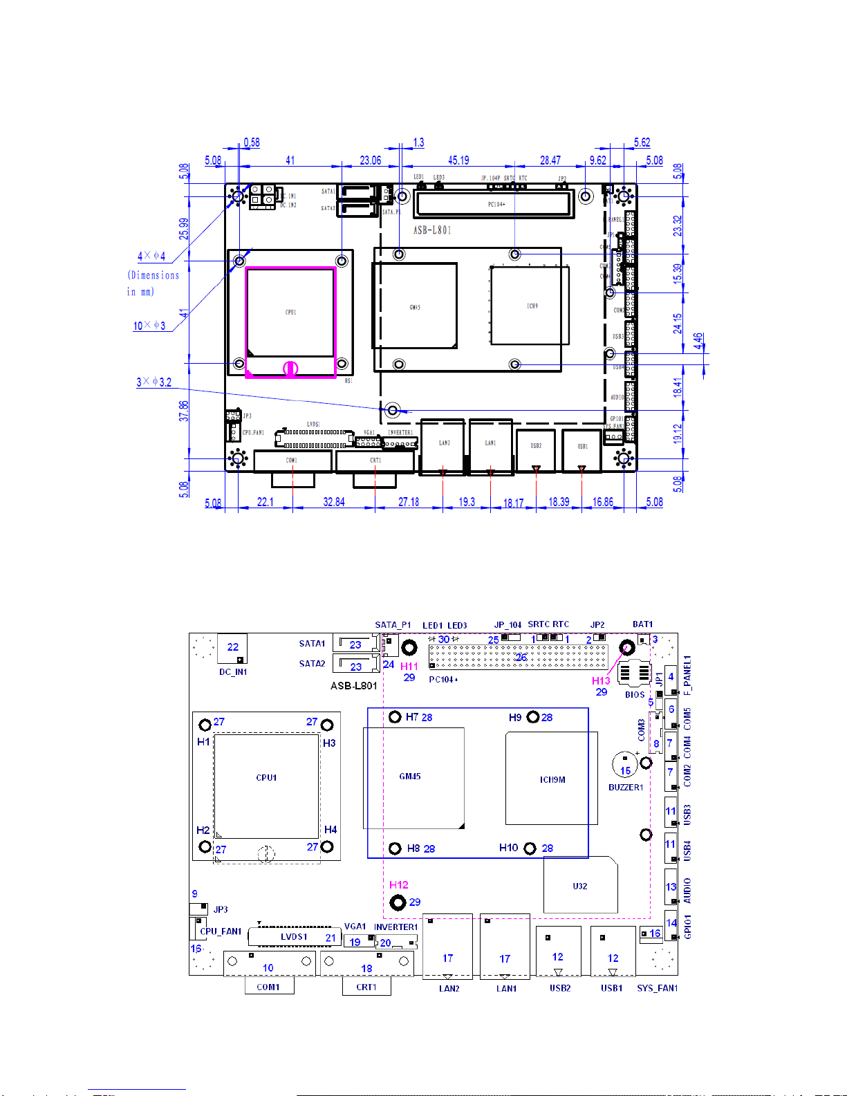
5.2 BOARD DIMENSIONS ..........................................................................................................7
5.3 JUMPERS AND CONNECTORS LOCATION .......................................................................7
5.4 JUMPERS SETTINGAND CONNECTORS..........................................................................8
1. RTC,SRTC....................................................................................................................8
2. JP2................................................................................................................................8
3. BAT1..............................................................................................................................9
4. F_PANEL1.....................................................................................................................9
5. JP1................................................................................................................................9
6. COM5............................................................................................................................9
7. COM2,COM4 ..............................................................................................................10
8. COM3..........................................................................................................................10
9. JP3..............................................................................................................................10
10. COM1..........................................................................................................................11
11. USB3,USB4 ................................................................................................................11
12. USB1,USB2................................................................................................................11
13. AUDIO.........................................................................................................................11
14. GPIO1.........................................................................................................................12
15. BUZZER1....................................................................................................................12
16. CPU_FAN1,SYS_FAN1..............................................................................................12
17. LAN1,LAN2.................................................................................................................12
18. CRT1...........................................................................................................................13
19. VGA1...........................................................................................................................13
20. INVERTER1................................................................................................................13
21. LVDS1.........................................................................................................................13

3
22. DC_IN2 .......................................................................................................................14
23. SATA1,SATA2 .............................................................................................................15
24. SATA_P1.....................................................................................................................15
25. JP_104........................................................................................................................15
26. PC104+.......................................................................................................................15
27. H1,H2,H3,H4...............................................................................................................15
28. H7,H8,H9,H10.............................................................................................................15
29. H11,H12,H13...............................................................................................................15
30. LED1,LED3.................................................................................................................15
31. MPCIE1.......................................................................................................................15
32. H5,H6..........................................................................................................................15
33. IDE_CF1 .....................................................................................................................15
34. DDR3 ..........................................................................................................................16
35. KB/MS.........................................................................................................................16
6 BIOS SETUP DESCRIPTION ....................................................................................................16
6.1 OPERATIONS AFTER POST SCREEN............................................................................16
6.2 BIOS SETUP UTILITY.......................................................................................................17
6.3 MAIN SYSTEM OVERVIEW..............................................................................................18
6.4 ADVANCED SETTINGS ....................................................................................................19
6.5 ADVANCED PCI/PNP SETTINGS.....................................................................................27
6.6 BOOT SETTINGS..............................................................................................................29
6.7 SECURITY SETTINGS......................................................................................................31
6.8 ADVANCED CHIPSET SETTINGS....................................................................................32
6.9 EXIT OPTIONS..................................................................................................................38

4
1 Packing List
Thank you for purchasing anAplex Product!
Open the motherboard package and check for the following items. If the motherboard or
accessories are found damaged or missing, please contact your distributor immediately.
●1 x ASB-L801 4” Embedded Motherboard
●1 x USB (dual ports) Cable
●2 x Serial (COM, DB9) Cable
●1 x SATA Cable
●1 x SATA Power Cable
●1 x PS/2-Keyboard/Mouse Cable
●1 x CD Driver
2 Disclaimer
The information in this document is subject to change without further notice. Please refer to your
vendor for the latest information. In no event shall Aplex Technology Inc. be liable for hidden
defects or damages of any kind, whether consequential or incidental, arising from improper use
or installation of the product.
3 Trademarks
Microsoft, MS-DOS and Windows are registered trademarks of Microsoft Corporation.
Atom are trademarks owned by Intel Corporation.
Other trademarks mentioned in this manual are owned by their respective holders.
4 Safety Notices
4.1 Before using the product, please read this manual carefully.
4.2 Please handle the motherboard with necessary ESD protection measures. For example,
when putting unused motherboard into the antistatic bag, please wear antistatic gloves
before touching the motherboard.
4.3 Never bend the motherboard.
4.4 It is better to hold the motherboard by its edges.
4.5 Avoid turning on and off the PC frequently to prevent possible damages to the motherbo-
ard.
4.6 Be sure to unplug the system before installing or removing onboard devices.

5
5 Introduction
ASB-L801 is a 4" industrial Embedded motherboard developed on the basis of Intel GM45+
ICH9M, which provides abundant peripheral interfaces to meet the needs of different customers.
Also, it features dual 1000M LAN port, 5-COM port and dual Mini PCIE configuration. To satisfy
the special needs of high-end customers, PC104+ port (capable of adjusting IO voltage) richer
extension functions. Due to its compact size, the product is widely used in various sectors of
industrial control.
5.1 Specifications
Specifications
Board Size
165mm x 115mm
CPU Support
Support Intel 45nm Core 2 Duo, Celeron M uFCPGA,
FSB667/800/1066
Chipset
Intel GM45 + Intel ICH9M
Memory Support
1x SO-DIMM (204pins), up to 2GB DDR3 800/1066MHz FSB
Graphics
Integrated Intel GMA 4500HD, DVMT 5.0 compliant
Super I/O
Winbond W83627UHG
BIOS
AMIBIOS
Storage
2 x SATA Connector
1 x Compact Flash II Slot
Network
2 x RJ-45 1000Mbps LAN Intel 82574L
USB
4 x USB 2.0 stack port for external
4 x USB 2.0 Pin header for internal
Serial
1 x RS232 port, DB9 connector for external (COM1),
pin 9 w/5V/12V/Ring select
1 x 422/485 select header for internal (COM3)
3 x RS232 header for internal (COM2,COM4,COM5)
Digital I/O
8-bit digital I/O by Pin header
4-bit digital Input
4-bit digital Output
Battery
Support CR2477 Li battery by 2-pin header
Audio
Support Audio via Realtek ALC662 HD audio decoder
Support Line-in, Line-out, MIC by 2x5-pin header
Keyboard /Mouse
1x PS2 keyboard/mouse by 1x6 box pin header
Expansion Bus
1x PC 104+ connector (PCI master 4, jumper for +3.3V & 5V select)
1x mini-PCI-express slot (half-size )

6
Power
Management
DC12V input
1 x 2-pin power input connector
Front I/O
by 2x5-pin header
Power on/off switch
Reset switch
Power LED status
HDD LED status
Buzzer
Watchdog Timer
Software programmable 1 –255 second by Super I/O
External I/O port
1 x COM Port (COM1)
4 x USB 2.0 Ports (stack)
2 x RJ45 GbE Port (10/100/1000Mbps)
1 x VGA Port
1 x VGA 2x8 Pin Header
Temperature
Operating: 0℃–60℃
Storage: -20℃–80℃
Humidity
5% - 95%, non-condensing, operating
Power
Consumption
12V /2.0A (Intel 575/2.0GHz processor with 2GB DDR3 DRAM)
12V /1.5A (Intel P8400/2.26GHz processor with 2GB DDR3 DRAM)
12V /2.6A (Intel T3100/1.9GHz processor with 2GB DDR3 DRAM)
EMI/EMS
CE/FCC class A

7
5.2 Board Dimensions
5.3 Jumpers and Connectors Location
Board Top

8
Board Bottom
5.4 Jumpers Setting and Connectors
1. RTC/SRTC: (2.0mm Pitch 1X2 Pin Header)CMOS clear jumper, CMOS clear
operation will permanently reset old BIOS settings to factory defaults.
RTC/SRTC
CMOS
OPEN
NORMAL (default)
CLOSE 1-2
Clear CMOS
Procedures of CMOS clear:
5.4.1.1 Turn off the system and unplug the power cord from the power outlet.
5.4.1.2 To clear the CMOS settings, use the jumper cap to close pins1 and 2 for about 3
seconds then reinstall the jumper clip back to pins open.
5.4.1.3 Power on the system again.
5.4.1.4 When entering the POST screen, press the <F1> or <DEL> key to enter CMOS
Setup Utility to load optimal defaults.
5.4.1.5 After the above operations, save changes and exit BIOS Setup.
2. JP2: (2.0mm Pitch 1X2 Pin Header),ATX Power and AT Power setting jumper.
JP2
Mode
Open
ATX Power Mode
Close
AT Power Mode

9
3. BAT1: (1.25mm Pitch 1X2 box Pin Header) 3.0V Li battery is embedded to provide
power for CMOS.
Pin#
Signal Name
Pin1
VBAT
PIN2
Ground
4. F_PANEL: (2.0mm Pitch 2X5 Pin Header), Front panel connector.
Signal Name
Pin#
Pin#
Signal Name
HD LED+
1
2
POWER LED+
Ground
3
4
Ground
Ground
5
6
SW+
RESET+
7
8
Ground
SPK+
9
10
SPK-
Pin1-3: HDD LED, They are used to connect hard disk activity LED. The LED blinks
when the hard disk is reading or writing data.
Pin2-4: POWER LED, They are used to connect power LED. When the system is
powered on or under S0/S1 state, the LED is normally on; when the system
is under S4/S5 state, the LED is off.
Pin5-6: POWER on/off Button, They are used to connect power switch button. The
two pins are disconnected under normal condition. You may short them
temporarily to realize system startup & shutdown or awaken the system from
sleep state.
Pin7-8: RESET Button, They are used to connect reset button. The two pins are dis-
connected under normal condition. You may short them temporarily to realize
system reset.
Pin9-10: BUZZER, They are used to connect an external buzzer.
Note:
When connecting LEDs and buzzer, pay special attention to the signal pola-
rity. Make sure that the connector pins have a one-to-one correspondence
with chassis wiring, or it may cause boot up failure.
5. JP1: (2.0mm Pitch 1x3 Pin Header) COM5 setting jumper, pin 1~3 are used to select
signal out of pin 10 of COM5 port.
JP1 Pin#
Function
Close 1-2
COM5 Pin10=+5V (default)
Close 2-3
COM5 Pin10=+12V (option)
6. COM5: (2.0mm Pitch 2X5 Pin Header), COM5 Port, standard RS232 ports are provided.
They can be used directly via COM cable connection.

10
Signal Name
Pin#
Pin#
Signal Name
DCD
1
2
RXD
TXD
3
4
DTR
Ground
5
6
DSR
RTS
7
8
CTS
RI
9
10
Jp1 Setting:
Pin1-2 : 5V (default)
Pin2-3:12V (option)
7. COM2/COM4: (2.0mm Pitch 2X5 Pin Header),COM2 COM4 Port, up to 2 standard
RS232 ports are provided. They can be used directly via COM cable connection.
Signal Name
Pin#
Pin#
Signal Name
DCD
1
2
RXD
TXD
3
4
DTR
Ground
5
6
DSR
RTS
7
8
CTS
RI
9
10
NC
8. COM3: (2.0mm Pitch 1x6 box Pin Header),it provides selectable RS422/RS485 serial
signal output.
RS422 Type (option)
RS485 Type (default)
Signal Name
Pin#
Pin#
Signal Name
422RX-
1
1
NC
422RX+
2
2
NC
422TX-
3
3
485-
422TX+
4
4
485+
Ground
5
5
Ground
+5V
6
6
+5V
9. JP3: (2.0mm Pitch 2x3 Pin Header),COM1 setting jumper, pin 1~6 are used to select
signal out of pin 9 of COM1 port.
JP3 Pin#
Function
Close 1-2
RI (Ring Indicator) (default)
Close 3-4
COM1 Pin9=+5V (option)
Close 5-6
COM1 Pin9=+12V (option)
10. COM1: (Type DB9),Rear serial port, standard DB9 serial port is provided to make a
direct connection to serial devices. COM1 port is controlled by pins No.1~6 of JP3,select
output Signal RI or 5V or 12v, For details, please refer to description of JP3.

11
Pin#
Signal Name
1
DCD# (Data Carrier Detect)
2
RXD (Received Data)
3
TXD (Transmit Data)
4
DTR (Data Terminal Ready)
5
Ground
6
DSR (Data Set Ready)
7
RTS (Request To Send)
8
CTS (Clear To Send)
9
JP1 Setting:
Pin1-2 : RI (Ring Indicator) (default)
Pin3-4 : 5V Standby power (option)
Pin5-6:12V Standby power (option)
11.USB3/USB4: (2.0mm Pitch 2X5 Pin Header) ,Front USB connector, it provides 4 USB
ports via a dedicated USB cable, speed up to 480Mb/s.
Signal Name
Pin#
Pin#
Signal Name
VCC(+5V)
1
2
VCC(+5V)
USB_DB-
3
4
USB_DA-
USB_DB+
5
6
USB_DA+
Ground
7
8
Ground
NC
9
10
Ground
Note:
Before connection, make sure that pinout of the USB Cable is in accordance with that
of the said tables. Any inconformity may cause system down and even hardware
damages.
12. USB1/2:(Double stack USB typeA), Rear USB connector, it provides up to 4 USB2.0
ports, speed up to 480Mb/s.
13. AUDIO: (2.0mm Pitch 2X6 Pin Header), Front Audio, An onboard Realtek ALC662

12
codec is used to provide high-quality audio I/O ports. Line Out can be connected to a
headphone or amplifier. Line In is used for the connection of external audio source via a
Line in cable. MIC is the port for microphone input audio.
Signal Name
Pin#
Pin#
Signal Name
VCC(+5V)
1
2
Ground
LINE_OUT_L
3
4
LINE_OUT_R
FRONT_JD
5
6
LINE1_JD
LINE_IN_L
7
8
LINE_IN_R
MIC_IN_L
9
10
MIC_IN_R
Ground
11
12
MIC1_JD
14. GPIO1: (2.0mm Pitch 2x5 Pin Header),General-purpose input/output port, it provides
a group of self-programming interfaces to customers for flexible use.
Signal Name
Pin#
Pin#
Signal Name
Ground
1
2
GPIO18_OUT1
GPIO20_OUT2
3
4
GPIO33_OUT3
GPIO34_OUT4
5
6
GPIO18_IN1
GPIO20_IN2
7
8
GPIO33_IN3
GPIO34_IN4
9
10
+5V
15. BZ: onboard buzzer.
16. CPU_FAN/SYS_FAN1: (2.54mm Pitch 1x3 Pin Header),Fan connector, cooling
fans can be connected directly for use. You may set the rotation condition of cooling fan
in menu of BIOS CMOS Setup.
Pin#
Signal Name
1
Ground
2
VCC
3
Rotation detection
Note:
Output power of cooling fan must be limited under 5W.
17. LAN1/2: (RJ45 Connector), Rear LAN port,2 standard 10/100/1000M RJ-45 Ethernet
ports are provided. Used Intel 82574L chipset ,LINK LED (green) and ACTIVE LED
(yellow) respectively located at the left-hand and right-hand side of the Ethernet port
indicate the activity and transmission state of LAN.

13
18. CRT1: (CRT Connector DB15),Video Graphic Array Port, provide high-quality video
output. they can not work at the same time for CRT and VGA1.
19. VGA1: (CRT 2.0mm Pitch 2X5 Pin Header), Video GraphicArray Port, Provide 2x5Pin
cable to VGAPort, they can not work at the same time for CRT and VGA1.
Signal Name
Pin#
Pin#
Signal Name
CRT_RED
1
2
Ground
CRT_GREEN
3
4
Ground
CRT_BLUE
5
6
VGA_EN
CRT_H_SYNC
7
8
CRT_DDCDATA
CRT_V_SYNC
9
10
CRT_DDCCLK
20. INVERTER1: (2.0mm Pitch 1x6 box Pin Header), Backlight control connector for
LVDS1.
Pin#
Signal Name
1
+DC12V
2
+DC12V
3
Ground
4
Ground
5
BKLT_EN
6
BKLT_CTRL
Note:
Pin6 is backlight control signal, support DC or PWM mode, mode select at
BIOS CMOS menu.
21. LVDS1: For 18/24 bit LVDS output connector, Fully supported by Intel GM45 chipset,
the interface features dual channel 18/24-bit output. Model name of the interface
connector is Hirose DF13-40DP-1.25V.
Signal Name
Pin#
Pin#
Signal Name
VDD5
2
1
VDD5
Ground
4
3
Ground
VDD33
6
5
VDD33
LB_D0_N
8
7
LA_D0_N
LB_D0_P
10
9
LA_D0_P
Ground
12
11
Ground

14
LB_D1_N
14
13
LA_D1_N
LA_D1_P
16
15
LA_D1_P
Ground
18
17
Ground
LB_D2_N
20
19
LA_D2_N
LB_D2_P
22
21
LA_D2_P
Ground
24
23
Ground
LB_CLK_N
26
25
LA_CLK_N
LB_CLK_P
28
27
LA_CLK_P
Ground
30
29
Ground
LVDS_DDC_DATA
32
31
LVDS_DOC_CLK
Ground
34
33
Ground
LB_D3_N
36
35
LA_D3_N
LB_D3_P
38
37
LA_D3_P
NC
40
39
NC
22. DC_IN2: (5.0mm 1x2 Pin Connector),DC12V System power input connector。
Pin#
Signal Name
1
+12V
2
Ground
DC_IN1: (2x2 box Pin Connector),DC12V System power input connector。
Pin#
Signal Name
1
Ground
2
Ground
3
+12V
4
+12V
Note:
Make sure that the voltage of power supply is DC(12±5%)V before power on, or it
may cause boot up failure and even system damage.

15
23. SATA1/2: (SATA 7P),SATA1,SATA2 SATA Connectors, Two SATA connectors are
provided, with transfer speed up to 3.0Gb/s.
24. SATA_P1: (2.5mm Pitch 1x2 box Pin Header),an onboard 5V output connector is
reserved to provide power for IDE/SATAdevices.
Pin#
Signal Name
1
+DC5V
2
Ground
Note:
Output current of the connector must not be above 1A.
25. JP_104: (2.0mm Pitch 1X3 Pin Header) PC104+ port voltage selection jumper,select
voltage for PCI-104 Plus device.
JVCCIO
PC104+ VCCIO Voltage
OPEN
Default
CLOSE 1-2
+3.3V PCI Card
CLOSE 2-3
+5V PCI Card
26. PC104+: (4x30 Pin), PC104 plus connector, it conforms to standard PC104+ specifi-
cation. Can expand support four PCI devices.
27. H1/H2/H3/H4: CPU FAN SCREW HOLES, Four screw holes for fixed CPU Cooler
assemble.
28.H7/H8/H9/H10: GM45+ICH9M Heat Sink SCREW HOLES, Four screw holes for intel
GM45 and ICH9M Heat Sink assemble.
29.H11/H12/H13:PC104+ CARD SCREW HOLES, Three screw holes for PC104+ card
assemble.
30.LED1/LED3: LED STATUS. LED1:Motherboard Standby Power Good status。
LED3: Motherboard CPU Power Good status.
31.MPCIE1: (30mmx30mm Socket 52Pin),mini PCIE socket, it is located at the bottom, it
supports mini PCI-E devices with USB2.0, SMBUS and PCI-E signal.
32.H5/H6:MPCIE1 SCREW HOLES, H5 for mini PCIE card (30mmx30mm Socket 52 Pin)
assemble. H6 Reserve.
33. IDE_CF1: (CF Card socket), it is located at the bottom of the board and serves as an
insert interface for Type I and Type II Compact Flash card. The operating voltage of CF

16
card can be set as 3.3V or 5V. The default setting of the product is 3.3V.
34. DDR3: (SO-DIMM 204Pin socket), DDRIII memory socket, the socket is located at the
bottom of the board and supports 204Pin 1.5V DDRIII 800/1066MHz FSB SO-DIMM
memory module up to 2G.
35. KB/MS: (2.0mm Pitch 1X6 box Pin Header), PS/2 keyboard and mouse port, the port
can be connected to PS/2 keyboard or mouse via a dedicated cable for direct used.
(R1.0 )
Pin#
Signal Name
1
KBDATA
2
MSDATA
3
Ground
4
+5V
5
KBCLK
6
MSCLK
6 BIOS Setup Description
6.1 Operations after POST Screen
After CMOS discharge or BIOS flashing operation, the system will display the following
screen for your further operation. Press F2 key to continue or F1 key to enter CMOS
Setup.
AMIBIOS© 2006 American Mega trends , Inc.
BIOS Date: 03/08/11 23:27:33 Ver: 08.00.15
CPU : Genuine Intel(R) CPU 575 @2.00GHz
Speed : 2.00 GHz
Press F11 for BBS POPUP
Initializing USB Controllers. . Done.
2013MB OK
Auto-Detecting Pri Master.. IDE Hard Disk
Pri Master : Hitachi HTS545016B9A300 PB0C64G
Ultra DMA –5, S.M.A.R.T. Capable and Status OK
Auto –detecting USB Mass Storage Devices ..
00 USB Mass storage devices found and configured
CMOS Settings Wrong
CMOS Data / Time Not Set
Press F1 to Run SETUP
Press F2 to load default values and continue
0085

17
After optimizing and exiting CMOS Setup, the POST screen displayed for the first time is as
follows and includes basic information on BIOS, CPU, memory, and storage devices.
AMIBIOS© 2009 American Mega trends , Inc.
BIOS Date: 03/08/11 23:27:33 Ver: 08.00.15
CPU : Genuine Intel(R) CPU 575 @2.00GHz
Speed : 2.00 GHz
Press DEL to Run Setup
Press F11 for BBS POPUP
Initializing USB Controllers. . Done.
2013MB OK
Auto-Detecting Pri Master.. IDE Hard Disk
Pri Master : Hitachi HTS545016B9A300 PB0C64G
Ultra DMA –5, S.M.A.R.T. Capable and Status OK
Auto –detecting USB Mass Storage Devices ..
00 USB Mass storage devices found and configured.
Checking NVRAM..
0085
Press F11 to load default values and continue 0085
Press F11key to enter Boot Menu during POST, as shown by the following figure.
Please select boot device:
Hitachi HTS545016B9A300
USB: USB Hotplug FDD
SATA:4M-CSS HAK40-004G
↑and ↓to move selection
ENTER to select Boot device
ESC to boot using defaults
6.2 BIOS SETUP UTILITY
Press [Del] key to enter BIOS Setup utility during POST, and then a main menu
containing system summary information will appear.

18
BIOS SETUP UTILITY
Main
Advanced
PCIPnP
Boot
Security
Chipset
Exit
System Overview
User [ENTER],[TAB]
or [SHIFT-TAB] to
Select a field
Use[+] or [-] to
configure system Time.
←Select Screen
↑↓ Select Item
+- Charge Field
Tab Select Field
F1 General Help
F10 Save and Exit
ESC Exit
AMIBIOS
Version : 08.00.15
Build Date : 03/08/11
ID : L801V010
Processor
Genuine Intel(R) CPU 575 @ 2.00GHz
Speed :2000MHz
System Memory
Size :1981MB
System Time [00:01:09]
System Date [Tue 03/08/2011]
v02.61 © Copyright 1985-2006 American Megatrends , Inc.
6.3 System Overview
BIOS SETUP UTILITY
Main
Advanced
PCIPnP
Boot
Security
Chipset
Exit
System Overview
User [ENTER],[TAB]
or [SHIFT-TAB] to
Select a field
Use[+] or [-] to
configure system Time.
←Select Screen
↑↓ Select Item
+- Charge Field
Tab Select Field
F1 General Help
F10 Save and Exit
ECS Exit
AMIBIOS
Version : 08.00.15
Build Date : 03/08/11
ID : L801V010
Processor
Genuine Intel(R) CPU 575 @ 2.00GHz
Speed :2000MHz
System Memory
Size :1981MB
System Time [00:02:26]
System Date [Tue 03/08/2011]
V02.61 © Copyright 1985-2006 American Mega trends , Inc.

19
System Time:
Set the system time, the time format is:
Hour : 0 to 23
Minute : 0 to 59
Second : 0 to 59
System Date:
Set the system date, the date format is:
Day: Note that the „Day‟ automatically changes when you set the date.
Month: 01 to 12
Date: 01 to 31
Year: 2009 to 2099
6.4 Advanced Settings
BIOS SETUP UTILITY
Main
Advanced
PCIPnP
Boot
Security
Chipset
Exit
Advanced Settings
Configure CPU
←Select Screen
↑↓ Select Item
Enter Charge Field
F1 General Help
F10 Save and Exit
ESC Exit
WARNING: Setting wrong values In below sections
may cause system to malfunction.
►CPU Configuration
►IDE Configuration
►Super IO Configuration
►Hardware Health Configuration
►ACPI Configuration
►AHCI Configuration
►MPS Configuration
►PCI Express Configuration
►Smbios Configuration
►USB Configuration
V02.61 © Copyright 1985-2006 American Mega trends , Inc.

20
6.4.1 CPU Configuration
BIOS SETUP UTILITY
Advanced
Configure advanced CPU settings
Module Version: 3F.10
For UP platforms,
Leave it enabled.
For DP/MP serves,
It may use to tune
Performance to the
Specific application.
←Select Screen
↑↓ Select Item
+- Charge Field
F1 General Help
F10 Save and Exit
ESC Exit
Manufacturer : Intel
Genuine Intel(R) CPU 575 @ 2.00GHz
Frequency :2.00GHz
FSB Speed : 668MHz
Cache L1 :32 KB
Cache L2 :1024 KB
Ratio Actual Value :L2
Hardware Prefetcher [Enabled]
Adjacent Cache Line Prefetch [Enabled]
Max CPUID Value Limit [Disabled]
Execute-Disable Bit Capability [Enabled]
Intel(R) C-SATAE tech [Disabled]
V02.61 © Copyright 1985-2006 American Mega trends , Inc.
Hardware Prefetcher: [Enabled]
[Disabled]
Adjacent Cache Line Prefetch:
[Enabled]
[Disabled]
Max CPUID Value Limit:
[Enabled]
[Disabled]
Execute-Disable Bit Capability:
[Disabled]
[Enabled]
Intel(R) C-SATAE tech: [Disabled]
[Enabled]
Table of contents
Other Aplex Motherboard manuals