Arcom SC88T User manual

Contents
Revision History . . . . . . . . . . . . . . . . . . . . . . . . . . . . . . . . . . . . . . . . . . . . . . . . . . . . . . . . . . . . . . .3
Section 1. Introduction . . . . . . . . . . . . . . . . . . . . . . . . . . . . . . . . . . . . . . . . . . . . . . . . . . . . . . . . . .5
Section 2. Circuit Description . . . . . . . . . . . . . . . . . . . . . . . . . . . . . . . . . . . . . . . . . . . . . . . . . . . .6
Section 3. STEbus Interface . . . . . . . . . . . . . . . . . . . . . . . . . . . . . . . . . . . . . . . . . . . . . . . . . . . . . .7
Section 4. Links and Options . . . . . . . . . . . . . . . . . . . . . . . . . . . . . . . . . . . . . . . . . . . . . . . . . . . . .10
Section 5. I/O Devices . . . . . . . . . . . . . . . . . . . . . . . . . . . . . . . . . . . . . . . . . . . . . . . . . . . . . . . . . . .13
Section 6. Memory Map . . . . . . . . . . . . . . . . . . . . . . . . . . . . . . . . . . . . . . . . . . . . . . . . . . . . . . . . .15
Section 7. Using the SC88T . . . . . . . . . . . . . . . . . . . . . . . . . . . . . . . . . . . . . . . . . . . . . . . . . . . . . .17
Appendix A. Component List . . . . . . . . . . . . . . . . . . . . . . . . . . . . . . . . . . . . . . . . . . . . . . . . . . . .19
Appendix B. Connections . . . . . . . . . . . . . . . . . . . . . . . . . . . . . . . . . . . . . . . . . . . . . . . . . . . . . . . .20
Appendix C. Specification . . . . . . . . . . . . . . . . . . . . . . . . . . . . . . . . . . . . . . . . . . . . . . . . . . . . . . .22
Appendix D. Example Program . . . . . . . . . . . . . . . . . . . . . . . . . . . . . . . . . . . . . . . . . . . . . . . . . . .23
Appendix E. Circuit Diagram . . . . . . . . . . . . . . . . . . . . . . . . . . . . . . . . . . . . . . . . . . . . . . . . . . . . .30
Page 1
J90 SC88T2192-08819-000-000
SC88T
STE 80188 CPU
Technical Manual

J90 SC88T
Page 2
2192-08819-000-000

Revision History
Page 3
J90 SC88T2192-08819-000-000
Manual
V1 Iss 2
Addendum
Issue A
Issue B
V1 Iss 2
V2 Iss 3
V2 Iss 3
870414 First Published in this format.
970818 ECO2630.
971103 ECO2674
PCB Comments
© Arcom Control Systems Ltd
Cambridge
1997
The choice of board or systems is the responsibility of the buyer, and the use to which they are put
cannot be the liability of Arcom Control Systems Ltd. However, Arcoms sales team is always
available to assist you in making your decision.
Product Information
Full information about other Arcom products is available via the Fax-on-Demand System, (Telephone
numbers are listed below), or by contacting our Website at: www.arcom.co.uk, or for the US,
www.arcomcontrols.com
Additional useful contact information:
Customer Support: (tel) +44 (0)1223 412428, (fax) +44 (0)1223 403400, (email) [email protected]
Sales: (tel) +44 (0)1223 411200, (fax) +44 (0)1223 410457, (email) [email protected], or for the US,
United Kingdom
Arcom Control Systems Ltd
Clifton Road
Cambridge
CB1 4WH
UK
tel: +44 (0)1223 411200
fax: +44 (0)1223 410457
FoD: 01223 240600
United States
Arcom Control Systems Inc
13510 South Oak Street
Kansas City, MO 64145
USA
tel: (toll free) 888-941-2224
fax: 816-941-7807
FoD: 800-747-1097
Germany
(Kostenlose Infoline:)
tel: 0130 824 511
fax: 0130 824 512
FoD: 0130 860 449
Italy
(Numeroverde:)
FoD: 1678 73600
Belgium
(Groen Nummer:)
tel: 0800 7 3192
fax: 0800 7 3191
Netherlands
(Gratis 06 Nummer:)
tel: 06022 11 36
fax: 06022 11 48
France
Arcom Control Systems
Centre d’affaires SCALDY
23, rue Colbert
7885 SAINT QUENTIN
Cedex, FRANCE
tel:(Numero Vert) 0800 90 84 06
fax:(Numero Vert) 0800 90 84 12
FoD:(Numero Vert) 0800 90 23 80

J90 SC88T
Page 4
2192-08819-000-000

Section 1. Introduction
The SC88T is a powerful and expandable single-board computer, based on the
Intel 80188 microprocessor. It is designed as a CPU board for CPU in a large
control system. It uses the industry-standard STEbus, so a large range of
peripheral boards are available.
Software allows programs written in Borland C to be put into an EPROM and
run on the SC88T without disks, and support for development on a PC. Contact
us for details.
The STEbus interface is an important feature of the SC88T. The bus is being
ratified by the IEEE (IEEE designation is P1000), and it is designed as a
processor- and manufacturer-independent, asynchronous, multiprocessing bus.
The asynchronous nature of the bus means that a slave board (memory or I/O)
must acknowledge commands by the SC88T, which will wait until it does, so
that any speed of peripheral board can be accessed by any speed of CPU board.
The multiprocessing ability lets you run several CPU boards on the same bus.
This is explained in greater detail later on.
Page 5
J90 SC88T2192-08819-000-000

Section 2. Circuit Description
The 16MHz oscillator module drives the 80188 CPU (IC12) and optionally the
STEbus system clock. The 8MHz output clock from the CPU is halved by IC11,
to produce the 4MHz clock to drive the SCC (IC13). The SCC is wired to
connector PL3 via RS232 buffer IC18 and IC19.
IC9 is a logic array which detects bus accesses and generates wait states, based
on the address, the state of the on-board chip selects and the CPU status. IC8
latches the top 4 bits of the CPU address bus and IC7 latches the lowest eight
bits. IC11 controls chip-selects for the RAMs (IC15,17) and generates a one bit
output port for use as an attention request on the STEbus.
The EPROMs (IC14 and 16) can be 8, 16, 32 or 64k each and there are 2 jumpers
to set the EPROM size.
Address and data lines on the bus are driven by IC1,2,4 and 5, with IC5 driving
the strobes. Incoming bus signals are buffered by IC3 and 6. Reset can come in
from the bus (via LK5A) to reset the CPU, or it can go to the bus from the on-
board reset circuit, in which case a reset switch can be wired between the pins
of connector PL2.
J90 SC88T
Page 6
2192-08819-000-000
Section 3. STEbus Interface
The SC8TT has a STEbus interface with the IEEE number P1000. Here is a
summary of the features of the bus with some notes on their implementation on
the SC88T board. The pinout of the bus is given in Appendix B.
Table 1. STEbus interface on the SC88T
Page 7
J90 SC88T2192-08819-000-000
Signal
A0 - A19
A0 - 11
A0 - 2
D0 - 7
ADRSTB*
DATSTB*
CM2
CM1
CM0
0
0
0
I/O
0
0
0
0
0
3s
3s
3s
3s
3s
3s
3s
3s
3s
20-bit memory
address
12-bit I/O address
3-bit acknowledge
address
8-bit data bus
Address Strobe
Data Strobe
Buffered from the CPU 20-bit address.
As above.
The SC88T does not handle bus-vectored
interrupts, so it does not generate
acknowledge cycles. It does respond to bus
non-vectored interrupts on lines ATNRQ0*-
ATNRQ3* if they have been appropriately
jumpered.
Driven by the CPU on write cycles, or by the
slave on read cycles.
Addresses, data and command modifiers are
valid before the falling edge of ADRSTB* and
DATSTB*. Both strobes are active at the same
time on the SC88T.
On the write cycle, valid data and CM0 are
present before this is asserted. On a read
cycle, CM0 height is present before it is
asserted and DATSTB* then indicates to the
slave that the CPU is ready to accept
Command modifiers indicating the type of
bus cycle, according to the following table:
CM 2 1 0
0 0 0 \
0 0 1 } reserved
0 1 0 /
0 1 1 acknowledge
1 0 0 I/O write
1 0 1 I/O read
1 1 0 memory write
1 1 1 memory read
(Note: the acknowledge cycle is NOT
generated by the SC88T.)
In-Out Type Description Implementation

Table 1. (continued)
The SC88T can be jumpered either to act as a potential master which requests
the bus from the permanent master or a separate arbiter, or it can be set up to
ignore arbitration. If the SC88T is set to ignore arbitration it must be the only
master on the bus. If you wish to use more than one master on the bus, then you
must have one and only one arbiter. A suitable arbiter is available on the
SYSCON board. See Links and Options for details of how to set up the board.
Key: * = signal is active low
3s = tri-dtate
tp = totem-pole
o/c = open-collector
It is quite easy to use the SC88T on the STEbus. You will need a terminated
backplane, and one or more slave boards, such as A/D converters, for example.
In order to comply fully with the specification of the impedance of each
backplane line should be 60 ohms ±10%. However, a short backplane is not
likely to cause any malfunction even if its impedance varies considerably from
this. A terminator is necessary because some of the lines are open-collector, and
timing is critical on the strobes.
A SC88T configured as standard will generate all necessary bus signals. All that
is required to generate a bus access is that you try to read from or write to a
memory or I/O location which the on-board logic defines as on the bus. See the
Memory Map and I/O Devices sections for details on which addresses are on-
board and which are not.
Note: The internal timers on the SC88T can be programmed so that if the slave
board which you are attempting to access does not respond, for example if you
used the wrong address, a bus timeout will be generated. This will release the
SC88T from its wait-state and generate an interrupt.
See section 7. for more details.
J90 SC88T
Page 8
2192-08819-000-000
Signal
BUSRQ0-1*
BUSAK0-1*
0
I
o/c
in
Bus requests
Bus Acknowledge
Potential (temporary) bus masters request the
bus from the arbiter on either of these lines.
BUSRQ0* has a higher priority than
BUSRQ1*.
The SC88T acts as temporary master, and can
be jumpered to ignore arbitration as a single
master.
The arbiter acknowledges a request from
either of the two potential masters on these
lines. A potential master may only drive the
bus when it has received an acknowledge on
the line corresponding to its request.
In-Out Type Description Implementation

If the SC88T HANGS on a bus access, or a bus timeout occurs, check the
following:
Are the address and data lines enabled (HUNG state)?
If they are not, the SC88T has not gained access to the bus. This may be
because some other master already has access to the bus and has not
released it. Check the state of the BUSRQ* and BUSAK* lines, and jumpers
LK2C and D.
If they are, check that DATACK* or TFRERR* has been received.
If DATACK* or TFRERR* have not been received (Bus timeout)
Check that the slave board can respond to the bus access which the SC88T
sent out.
If it can, check the SYSCLK is present on the bus, as many slave boards
require this for timing, and check also that SYSCLK is coming from only
one source, if you have more than one CPU on the bus.
Check also that your software has allowed bus timeouts to occur, and that it can
deal with interrupts from bus timeouts if they happen. It may sometimes be
useful to disable bus timeouts and check the bus in the HUNG state if you are
confused.
Page 9
J90 SC88T2192-08819-000-000
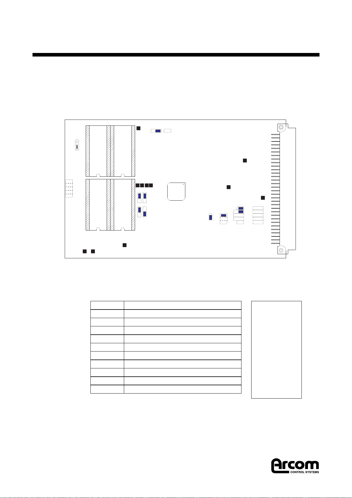
Section 4. Links and Options
There are many different ways in which you can configure the SC88T; they are
selected by jumpering across the links on the board. A + indicates a default link
setting. The board is described as seen from the component side of the board,
with the 64-way bus connector to the right.
Figure 1. Link Positions
Link area 1 Attention Requests in and out
J90 SC88T
Page 10
2192-08819-000-000
TP3
TP4
LK5 PL2
TP1
TP8
LK6A
B
A
B
A
B
A
B
A
B
LK7
LK9 LK8
TP9
TP10
TP11
A B
TP6 TP7
LK4
LK2 LK1
A
B
C
A
B
C
D
E
A
B
C
D
E
LK3
1 2 1 2
PL1
PL3
LK10
TP2
TP5
LK1A1
LK1A2
LK1B1
LK1B2
LK1C1
LK1C2
LK1D1
LK1D2
LK1E1
LK1E2
LK1DE2
/ATOUT to ATNRQ1*
ATNRQ1* goes to CPU INT0
/ATOUT to ATNRQ2*
ATNRQ2* goes to CPU INT1
/ATOUT to ATNRQ3*
ATNRQ3* goes to CPU INT3
/ATOUT to ATNRQ5*
ATNRQ5* goes to CPU DRQ0
ATNRQ7* goes to CPU DRQ1
ATNRQ6* goes to CPU DRQ1
ATNRQ6* goes to CPU DRQ0
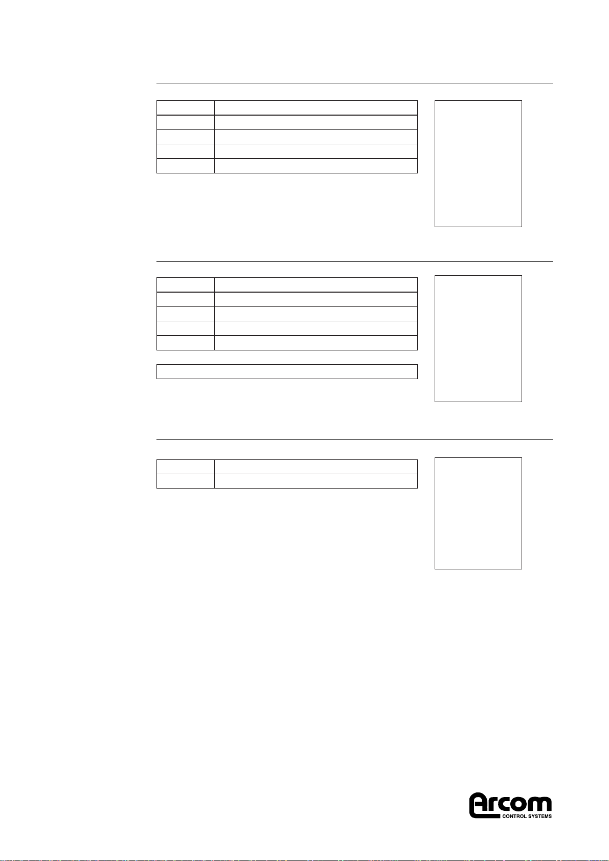
Figure 2.
Link area 1.
o A1 o A2 o
o B1 o B2 o
o C1 o C2 o
o D1 o D2 o
DE2
o E1 o E2 o

Link area 2 Reset, Bus Requests/Acknowledges, Clock.
Notes:
If LK2B2 is made, the state of LK2C and D is irrelevant.
If LK2B2 is made, an external arbiter cannot be used, and the SC88T must be the
only master on the STEbus.
The request and acknowledge must be on the same level if an external arbiter is
used. This means that if LK2C1 is made, LK2D1 must also be made.
Alternatively, if LK2C2 is made, LK2D2 must also be made.
Link area 3 Non-Maskable Interrupts (NMIs)
Link area 4 RAM size
Link area 5 Board reset
Page 11
J90 SC88T2192-08819-000-000
+ LK2A
LK2B1
+ LK2B2
LK2C1
LK2C2
LK2D1
LK2D2
LK2E
SYSRST* to bus from this board
Accept bus acknowledges from
external arbiter
Ignore arbitration, single master only
Bus requests on BUSRQ1*
Bus requests on BUSRQ0*
Bus acknowledges on BUSACK1*
Bus acknowledges on BUSACK0*
SYSCLK from this board
+ LK3A
LK3B
LK3C
NMI disabled
NMI from ANRQ0*
NMI from TFRERR*
+ LK4 open
LK4 made
8k RAM chips installed
(e.g. 6264 or similar)
32k RAM chips installed
(e.g. 55257 or similar)
LK5A
+ LK5B This board is reset from the STEbus
This board is reset from a switch
across PL2
Figure 3.
Link area 2.
o A o
o B1 o B2 o
o C1 o C2 o
o D1 o D2 o
o E o
Figure 4.
Link area 3.
o A o
o B o
o C o
Figure 5.
Link area 4.
o
o
Figure 6.
Link area 5.
o A o B o
Link area 6 and 7 EPROM pins
Link area 8 and 9 RAM pins
Link area 10 Serial Input level on channel A
Note: This link is hardwired in the B position. You must take care if the A position is
used: If RS232 levels are input in the A position, SCC will be destroyed.
J90 SC88T
Page 12
2192-08819-000-000
+ LK6A
LK6B
+ LK7A
LK7B
EPROMs pin 1 to +5V (all except 27512)
EPROMs pin 1 to A15 (27512 only)
EPROMs pin 27 to +5V (2764 & 27128)
EPROMs pin 27 to A14 (27256 & 27512)
LK8A
+ LK8B
+ LK9A
LK9B
NB: LK9 Dependant on LK8
RAM power is from STEbus VSTBY line
RAM power is from on-board +5V
RAM pin 26 to +5V (8k RAMs or VSTBY)
RAM pin 26 to A13 (32k RAMs)
Figure 7.
Link areas 6
and 7
o o
7A 6A
o o
7B 6B
o o
Figure 8.
Link areas 8
and 9
o o
9A 8A
o o
9B 8B
o o
LK10A
+ LK10B Serial input is at TTL levels
Serial input is at RS232 levels
Figure 9.
Link area 10
o
A
o
B
o

Section 5. I/O Devices
The chip-selects for I/O devices are generated by the 80188, and it is vital to set
the 80188 up in software as part of the initialisation sequence. If this is not done
the board will not function correctly. See section 7 for information on how to do
this.
There are three types of I/O devices which the 80188 can access.
1. I/O boards on the STEbus
The STEbus 4k I/O space is accessed in the lower 32k of the 80188s 64k I/O
address space. The selection is automatic, and the programmer should not
relocate any of the programmable I/O chip selects in this space.
2. The on-board SCC for serial communications
The on-board SCC is controlled by two programmable chip-selects. PCS1 is the
chip-select which accesses the registers. Accessing PCS2 will assert INTA*, the
SCC interrupt acknowledge input. This must be done to acknowledge the SCC
interrupt generated on INT2 of the 80188, because the 80188 in its most useful
interrupt mode does not generate an acknowledge. A read from PCS2 will read
the interrupt vector from the SCC and reset the SCC ready for the next interrupt.
3. The 80188 on-chip peripherals (counter/timers, DMA etc)
These integrated peripherals (and the address of PCS1 and PCS2) are controlled
by the Internal Control Block. Even the I/O base location of this block of
peripherals is controlled by the relocation register within the block. It is
recommended that you do not alter this block unless you are sure what you are
doing.
Page 13
J90 SC88T2192-08819-000-000
Internal block control register map
After a reset, the 256-byte Internal Control Block base address will be at FF00
(Hex) in I/O space. The individual control registers reside within the block, at
fixed-offsets from the base address. Each register is 16-bits wide.
Note that programming the control block is not a trivial task. More detailed
information on how to do this may be found in the Intel 80188 data book. This
manual covers values for most useful memory maps for the SC88T.
If PACS is loaded with OFBE and MPCS is loaded with 80B8 then the Peripheral
Chip Select map appears as below.
J90 SC88T
Page 14
2192-08819-000-000
Base +offset
FF00 +20 to +3E
+50 to +56
+58 to +5E
+60 to +66
+A0
+A2
+A4
+A6
+A8
+C0 to +CA
+D0 to +DA
+FE
UMCS
LMCS
PACS
MMCS
MPCS
Interrupt Controller
Timer 0 Control
Timer 1 Control
Timer 2 Control
Upper Memory Chip Select
Lower Memory Chip Select
Peripheral Base Address Control
Middle Memory Chip Select
Middle Peripheral Chip Select
DMA Descriptors Channel 0
DMA Descriptors Channel 1
Relocation register
Control Block register
Base +offset
F800 +000
+080
081
082
083
+100
+180
+200
+280
+300
+380
PCS0
PCS1
PCS2
PCS3
PCS4
PCS5
PCS6
PCS7
not used
SCC channel B control
SCC channel A control
SCC channel B data
SCC channel A data
Read to generate INTA* and fetch vector
from the SCC (i.e. the interrupt acknowledge
address)
Writing a byte with D0 = 1 asserts /ATOUT
(low) Do not read, as D0 will not be
predictable.
not used
not used
not used
not used
Peripheral Chip Select I/O map

Section 6. Memory Map
The 80188 CPU has several programmable chip-select lines, which are asserted
when the CPU address falls within the chip-select boundaries defined in the
CPUs internal chip select registers. Upon reset, the 80188 asserts the Upper
Memory-Chip Select (UCS) to select EPROM1 (IC16), and jumps to location
0FFFF0H. The first instructions must be to re-set the Upper Memory Chip Select
register (UMCS) as in the table below, then jump to some code lower in (IC16).
This code can then set up the MMCS and MPCS registers, by which time both
EPROMS will be properly selected. An example of this is given at the end of the
assembly language program in Appendix D.
If EPROM0 (IC14) is not to be used then it will not be enabled if the MMCS
register is left unaccessed. If IC14 is to be used, then using the values in the table
below , EPROM0 will occupy memory directly below IC16, forming a
contiguous block. This also imposes the restriction that EPROM0 and EPROM1
must be the same size.
Because UCS overlaps MCS3, the number of programmable wait states must be
identical for the UCS and MCSO-3 . Two wait-states will be required by slow
EPROMs. If STEbus memory overlaps MCS1 and MCS0 then MCS0-3 must
accept externally generated wait-states until DATACK* is received from the bus
. Both the above conditions are satisfied by the contents of the table below. Slow
EPROMs are those of 250ns access time and above. Note that Arcom use two
wait-states in their initialisation code. This allows the use of any EPROM
currently available.
The RAM is selected by the Lower Memory Chip-Select (LCS), which may be set
from 8k (one 8k RAM) to 64k (two 32k RAMs). Wait-states are not usually
required for fast static RAMs.
If a memory access is made to an address which is within neither UCS, MCS2 or
LCS, the STEbus will be selected automatically. This may result in a bus timeout
if no actual memory exists on the bus. The tables below contain chip select
register values for various RAM and EPROM sizes. EPROM IC16 and IC14 must
be the same size.
Page 15
J90 SC88T2192-08819-000-000
Total EPROM
capacity
16k
32k
64k
128k
2764 8k
27128 16k
27256 32k
27512 64k
FE3E
FC3E
F83E
F03E
F802
F002
E002
C002
8438
8838
9038
A038
Individual
EPROM type,
size
Register contents (hex)
UMCS MMCS MPCS
Total RAM
8k
16k
32k
64k
6264
6264
55257
55257
----
6264
-----
55257
01F8
03F8
07F8
0FF8
IC15 IC17 LMCS

The memory blocks of the 80188 cannot be
mapped at any arbitrary location. The
Middle Memory Chip-Selects are all the
same size, and must be mapped at a base
address which is a multiple of the middle
memory block size. Hence this is the only
way of creating a chip select area contiguous
with UCS.
MCS0, MCS1 and MCS3 are not used. To
ensure that they do not interfere with STE
memory space, set UCS and MCS0-3 to
include externally -generated wait states. (So
that accesses to memory in the MCS0 and
MCS1 address ranges wait for the DATACK*
signal from the STEbus.)
Example shown with two 8k RAMs (as
supplied) plus two 32k EPROMs.
J90 SC88T
Page 16
2192-08819-000-000
Example memory map using two 32k EPROMs. If EPROM 0 is not used, and
MCS0-3 disabled, then STEbus accesses may continue up to the base address of
EPROM1.

Section 7. Using the SC88T
Because the SC88T can be configured in so many different ways, it is difficult to
make any general recommendation about using it, mainly because the software
will determine how it is used. There are two obvious situations where it can be
employed, and a summary of them may suggest other possibilities.
As a target system
Here the SC88T runs software created on another computer, which is
transferred either by blowing an EPROM or by downloading machine-code into
RAM. A useful approach is to have a machine-code monitor in the EPROM
socket, so that the code can be debugged.
If you want to start from scratch the following notes may help.
The chip-select for EPROM (UCS) should be set up first, so that you can jump to
the start of EPROM and then continue initialising.
The LCS is required before any stack or memory operations are done with the
on-board memory.
The peripheral chip-selects must be programmed to allow access to the on-
board SCC.
Timers 0 and 1 may be programmed to produce a bus timeout function. The
input to T0 is the bus driver enable line; T0 output is wired to T1 input, and T1
output going low will take the CPU out of the wait-state. For this to happen it is
necessary to set T0 up as a free-running timer which is stopped by the active-
low bus-driver enable signal: T1 must be set up to be retriggered by pulses on
its input (which is connected to T0 output). If T1 then fails to be retriggered to
T0 it will time out. It can also generate an interrupt when it times out so that the
CPU is aware that a timeout has occurred.
The SCC requires some initialisation code, and it is strongly recommended that
you obtain the SCC Technical Manual before doing anything unusual.
If 80188 instructions are used in test and set operations for communication
between processors on the bus, they should be prefixed with the LOCK prefix.
This will prevent the bus request from going away until the instruction is
complete.
Page 17
J90 SC88T2192-08819-000-000

J90 SC88T
Page 18
2192-08819-000-000

Appendix A. Component List
Page 19
J90 SC88T2192-08819-000-000
LK10B Cable Misc, Solid Wire Tin Copper 22swg
64PCB 964-053
Bergstick 1 row
Bergstick 1 row
Bergstick 1 row
Bergstick 1 row
Bergjump
Bergstick 2 row
Bergstick 2 row
Bergstick 2 row
Bergstick 2 row
PCB Test point loop
Brass Hot Tin
28 Pin TP
16 MHz Half Size
22U 16V 10% CASE-D
3U3 16V 10% CASE-B
10U 16V CASE-B
8530 SCC 6MHz ZILOG PLCC
14C89
14C88 Texas Only
80C188-16 CMOS
S04
LS245
HCT373
1206 CASE 31R at 100MHz
4.7uH 900Ma CASE 2220
10K DIL 4 IND ROHM MNR34
10K DIL 4 IND ROHM MNR34
Single 1N4148
BAR43S 2x SCHOTTKY SOT23
NCHANNEL MOSFET2N7002
1N0 10% 50V 0805
100N 10% 50V 0805
180P 10% 0805
220P 10% 50V 0805
33R 5% 1/8W
1K0 5% 1/8W
4K7 5% 1/8W
10K 5% 1/8W
330R 5% 1/8W
47K 5% 1/8W 1206
100R 5% 1/8W
2K2 5% 1/8W
16V8-25 PLCC
16V8-25 PLCC
Conn Multi, 41612
Conn Multi, Inter-PCB
Conn Multi, Inter-PCB
Conn Multi, Inter-PCB
Conn Multi, Inter-PCB
Conn Multi, Inter-PCB
Conn Multi, Inter-PCB
Conn Multi, Inter-PCB
Conn Multi, Inter-PCB
Conn Multi, Inter-PCB
Conn Terminals/Test Lead
Fastening, Rivet
Socket IC TH, Misc
XTAL Th, Module
CAP SM, TANT
CAP SM, TANT
CAP SM, TANT
IC Interface SM, Periph
IC Interface SM, Periph
IC Interface SM, Periph
IC Processor Th, STD
IC STD Logic SM, TTL
IC STD Logic SM, TTL
IC STD Logic SM, HCT
Inductor SM , Misc
Inductor SM , Misc
RES Fixed SM, Network
RES Fixed SM, Network
Semi SM, Diode
Semi SM, Diode
Semi SM, Trans
CAP SM, Ceramic
CAP SM, Ceramic
CAP SM, Ceramic
CAP SM, Ceramic
RES Fixed SM, 1206
RES Fixed SM, 1206
RES Fixed SM, 1206
RES Fixed SM, 1206
RES Fixed SM, 1206
RES Fixed SM, 1206
RES Fixed SM, 1206
RES Fixed SM, 1206
IC PLD SM, Misc
IC PLD SM, Misc
PL1
LK1-1 (A-E>
LK2-1 (B-D)
LK4-9
PL2
MISC
LK1-2 (A-E)
LK2-2 (A-E)
LK3
PL3
TP1-11
MISC
IC14-17
XM1
C2, 3, 33, 34
C35
C36, 37
IC13
IC18
IC19
IC12
IC3, 6, 10
IC1, 2, 4, 5
IC7, 8
L1-20
L21, 22
RP3+6
RP1+4, RP2+5
D1, 2
D3
TR1, 2
C1
C14-32, 38, 39
C4
C5-13
R9-11
R4, 7
R1
R13-15
R12
R6
R5, 16, 17
R2, 3, 8
IC11
IC9
1
1
0.2
0.1
0.5
0.1
13
0.2
0.2
0.1
0.2
11
2
4
1
4
1
2
1
1
1
1
3
4
2
20
2
2
4
2
1
2
1
21
1
9
3
2
1
3
1
1
3
3
1
1
Appendix B. Connections
There are three connectors on the board. Pin 1 of each connector is marked, and
they are shown here as they appear on the board.
PL1
STEbus 64-way a/c DIN41612
J90 SC88T
Page 20
2192-08819-000-000
Pin
1
2
3
4
5
6
7
8
9
10
11
12
13
14
15
16
17
18
19
20
21
22
23
24
25
26
27
28
29
30
31
32
gnd o o gnd
+5V o o +5V
D0 o o D1
D2 o o D3
D4 o o D5
D6 o o D7
A0 o o gnd
A2 o o A1
A4 o o A3
A6 o o A5
A8 o o A7
A10 o o A9
A12 o o A11
A14 o o A13
A16 o o A15
A18 o o A17
CM0 o o A19
CM2 o o CM1
ADRSTB* o o gnd
DATACK* o o DATSTB*
TRFERR* o o gnd
ATNRQ0* o o SYSRST*
ATNRQ2* o o ATNRQ1*
ATNRQ4* o o ATNRQ3*
ATNRQ6* o o ATNRQ5*
gnd o o ATNRQ7*
BUSRQ0* o o BUSRQ1*
BUSAK0* o o BUSAK1*
SYSCLK o o VSTBY
-12V o o +12V
+5V o o +5V
gnd o o gnd
Row
a c
Table of contents
Other Arcom Motherboard manuals


 manual")


