Arcom VIPER User manual

VIPER Contents
VIPER
Intel PXA255 XScale RISC based
PC/104 Single Board Computer
Technical Manual
www.arcom.com

VIPER Contents
Definitions
Arcom is the trading name for Arcom Control Systems Inc and Arcom Control Systems Ltd.
Disclaimer
The information in this manual has been carefully checked and is believed to be accurate. Arcom assumes no responsibility
for any infringements of patents or other rights of third parties, which may result from its use.
Arcom assumes no responsibility for any inaccuracies that may be contained in this document. Arcom makes no commitment
to update or keep current the information contained in this manual.
Arcom reserves the right to make improvements to this document and /or product at any time and without notice.
Warranty
This product is supplied with a full 3 year warranty. Product warranty covers failure caused by any manufacturing defects.
Arcom will make all reasonable effort to repair the product or replace it with an identical variant. Arcom reserves the right to
replace the returned product with an alternative variant or an equivalent fit, form and functional product. Delivery charges will
apply to all returned products. Please go to www.arcom.com/support for information about Product Return Forms.
Trademarks
ARM and StrongARM are registered trademarks of ARM Ltd.
Intel and XScale are trademarks or registered trademarks of Intel Corporation or its subsidiaries in the United States and
other countries.
Windows CE .NET is a trademark of the Microsoft Corporation.
CompactFlash is the registered trademark of SanDisk Corp.
Linux is a registered trademark of Linus Torvalds.
RedBoot and Red HatTM is a registered trademark of Red Hat Inc.
VxWorks is a register trademark of Wind River.
Bluetooth is a registered trademark of Bluetooth SIG, Inc.
All other trademarks recognized.
Revision History
Manual PCB Date Comments
Issue A
Issue B
Issue C
Issue D
Issue E
Issue F
Issue G
Issue H
V1 Issue 3
V1 Issue 3
V1 Issue 4
V1 Issue 5
V1 Issue 6
V1 Issue 6
V1 Issue 6
V1 Issue 6
26th June 2003
8th July 2003
14th August 2003
14th October 2003
11th December 2003
11th February 2004
14th May 2004
15th July 2004
First full release of Manual
Minor editorial changes
Content update
Minor changes
Update for new PCB Issue
Minor changes
Major technical information enhancements, updated layout
Minor changes
© 2004 Arcom.
Arcom is a subsidiary of Spectris plc.
For contact details, see page 72.
Arcom operates a company-wide
quality management system,
which has been certified by the
British Standards Institution (BSI)
as compliant with ISO9001:2000

VIPER Contents
Contents
Introduction ........................................................................................................................................4
VIPER ‘at a glance’ ................................................................................................................5
VIPER features ......................................................................................................................6
VIPER support products ........................................................................................................8
Handling your board safely ....................................................................................................9
Conventions .........................................................................................................................10
Getting started .................................................................................................................................11
Using the VIPER ..................................................................................................................11
Detailed Hardware Description ........................................................................................................13
VIPER block diagram...........................................................................................................13
VIPER address map ............................................................................................................14
Translations made by the MMU ...........................................................................................15
PXA255 processor ...............................................................................................................16
PXA255 GPIO pin assignments...........................................................................................17
Real Time Clock...................................................................................................................21
Watchdog timer ....................................................................................................................22
Memory ................................................................................................................................23
Interrupt assignments ..........................................................................................................25
Flat panel display support ....................................................................................................29
Audio....................................................................................................................................38
General purpose I/O ............................................................................................................39
USB interface.......................................................................................................................42
10/100BaseTX Ethernet.......................................................................................................43
Serial COMs ports................................................................................................................45
PC/104 interface ..................................................................................................................48
JTAG and debug access......................................................................................................49
Power and power management .......................................................................................................51
Power supplies.....................................................................................................................51
Power management.............................................................................................................52
Connectors, LEDs and jumpers .......................................................................................................59
Connectors...........................................................................................................................60
Status LED’s ........................................................................................................................69
Jumpers ...............................................................................................................................70
Appendix A – Contacting Arcom.......................................................................................................72
Appendix B – Specification ..............................................................................................................73
Appendix C - Mechanical diagram ...................................................................................................74
Appendix D - Reference information................................................................................................75
Appendix E - Acronyms and Abbreviations ......................................................................................77
Index ................................................................................................................................................78

VIPER Introduction
Introduction
The VIPER is an ultra low power PC/104 compatible single board computer based on
the Intel 400MHz PXA255 XScale processor. The PXA255 is an implementation of the
Intel XScale micro architecture combined with a comprehensive set of integrated
peripherals including, a flat panel graphics controller, DMA controller, interrupt
controller, real time clock and multiple serial ports. The VIPER board offers a wide
range of features making it ideal for power sensitive embedded communications and
multimedia applications.
The board is available in the following standard variants:
VIPER-400-M64-F32: Intel XScale TM PXA255 400MHz microprocessor, 64MByte
SDRAM, 32MByte FLASH.
•
•
•
•
VIPER-400-M64-F16: Intel XScale TM PXA255 400MHz microprocessor, 64MByte
SDRAM, 16MByte FLASH.
VIPER-400-M64-F32-I: Intel XScale TM PXA255 400MHz microprocessor, 64MByte
SDRAM, 32MByte FLASH, Industrial temperature range.
VIPER-400-M64-F16-I: Intel XScale TM PXA255 400MHz microprocessor, 64MByte
SDRAM, 16MByte FLASH, Industrial temperature range.
For alternative memory configurations, please contact Arcom.
© 2004 Arcom Issue H 4
VIPER Introduction
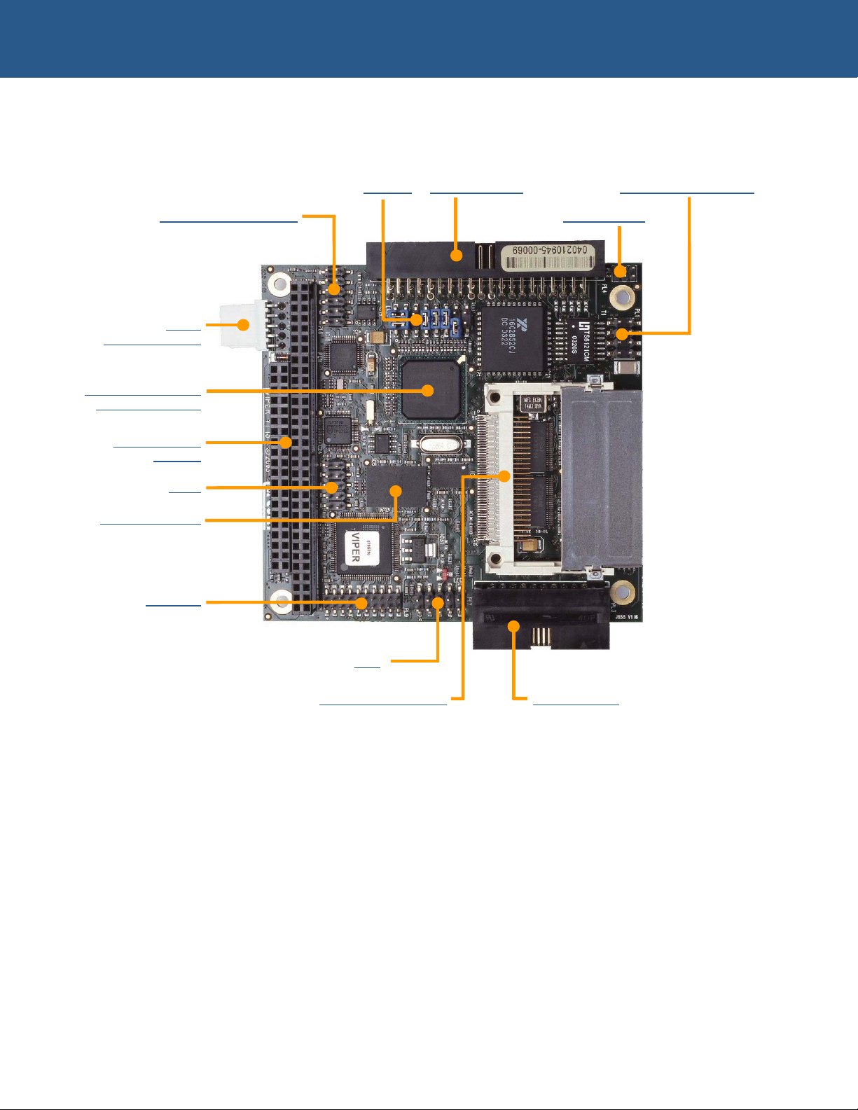
VIPER ‘at a glance’
Jumpers Five Serial Ports 10/100BaseTX Ethernet
Audio – In/Out/MIC/AMP Ethernet LEDs
Powe
r
(inc battery input)
Intel PXA255 XScale
400MHz processo
r
8/16-bit PC/104
interface
USB
CompactFLASH (CF+) TFT/STN panel
JTAG
Intel StrataFLASH
Digital I/O
© 2004 Arcom Issue H 5

VIPER Introduction
VIPER features
Microprocessor
Intel XScaleTM PXA255 400MHz RISC processor•
•
•
•
•
•
•
•
•
•
•
•
•
•
•
•
•
•
•
•
Cache
32K data cache, 32K instruction cache, 2K mini data cache
System memory
Up to 64MByte un-buffered 3.3V SDRAM
Silicon disk
Up to 32MByte Intel Strata FLASH (with FLASH access LED)
1MByte Bootloader FLASH EPROM (with FLASH access LED)
256KByte SRAM (with external battery backup)
Type I/II CompactFLASH (CF+) socket
Video
TFT/STN (3.3V or 5V – factory fit) flat panel graphics controller
Up to 800X600 resolution
8/16bpp
Backlight Control
Audio
National Semiconductor A AC’97 CODEC (16bit) and LM4880 Power Amp
Line IN, Line OUT, Microphone and 250mW per channel amplified output
Serial ports
5 x 16550 compatible high-speed UARTs
4 x RS232 and 1 x RS422/485 Interfaces
2 x channels with 128Byte Tx/Rx FIFO
USB host interface
Two USB 1.1 compliant interfaces
Short circuit protection and 500mA current limit protection
Network support
SMSC LAN91C111 10/100BaseTX Ethernet controller
One 10/100BaseTX NIC port
© 2004 Arcom Issue H 6

VIPER Introduction
Real Time Clock (RTC)
Battery backed RTC (external battery)•
•
•
•
•
•
•
•
•
•
•
•
± 1minute/month accuracy, at 25°C.
Watchdog
Adjustable timeout of 271ns to 19 minutes, 25 seconds
General Purpose I/O (GPIO)
8 x 5V tolerant Inputs
8 x 3.3V Outputs (5V tolerant)
User configuration
1 user-configurable jumper
Expansion
PC/104 expansion bus - 8/16 bit ISA bus compatible interface
JTAG port
Download data to FLASH memory
Debug and connection to In-Circuit Emulator (ICE)
Power
Typically 2W from a single 5V supply
Power Management features allowing current requirements to be as low as
107mA ±5mA (535mW ±25mW).
Size
PC/104 compatible footprint 3.8” x 3.6” (96mm x 91mm)
© 2004 Arcom Issue H 7

VIPER Introduction
VIPER support products
The VIPER is supported by the following products:
VIPER-UPS (Uninterruptible Power Supply)
The VIPER-UPS serves as a 5V DC power supply and battery back up system for
the VIPER. The UPS accepts between 10 – 36 VDC (10-25VAC) input and
generates the +5V supply for the VIPER. In addition to this, it includes an intelligent
battery charger/switch capable of using either the onboard 500mAHr NiMH battery
or an external sealed lead acid rechargeable battery. For further details, see
www.arcom.com/products/icp/pc104/processors/viper_UPS.htm.
•
VIPER-ICE (Industrial Compact Enclosure)
The VIPER-ICE is a simple low cost aluminum enclosure, which provides easy
connection to all on board features. The enclosure includes the VIPER-UPS and
optionally a color Q-VGA (320x240) TFT flat panel display and analog touch screen.
•
• VIPER-FPIF1 (Flat Panel Interface)
The VIPER-FPIF1 is a simple board that enables easy connection between the
VIPER and an LCD flat panel. See section VIPER-FPIF1 details, page 33 for further
details. Contact Arcom (see Appendix A – Contacting Arcom, page 72) for
purchasing information.
© 2004 Arcom Issue H 8

VIPER Introduction
Handling your board safely
Anti-static handling
This board contains CMOS devices that could be damaged in the event of static
electricity discharged through them. At all times, please observe anti-static precautions
when handling the board. This includes storing the board in appropriate anti-static
packaging and wearing a wrist strap when handling the board.
Packaging
Please ensure that should a board need to be returned to Arcom, it is adequately
packed, preferably in the original packing material.
Electromagnetic compatibility (EMC)
The VIPER is classified as a component with regard to the European Community EMC
regulations and it is the users responsibility to ensure that systems using the board are
compliant with the appropriate EMC standards.
© 2004 Arcom Issue H 9

VIPER Introduction
Conventions
Symbols
The following symbols are used in this guide:
Symbol
Explanation
Note - information that requires your attention.
Tip - a handy hint that may provide a useful
alternative or save time.
Caution – proceeding with a course of action may
damage your equipment or result in loss of data.
Jumper fitted on pin A.
Jumper fitted on pin B.
Jumper is fitted.
Jumper is not fitted.
B
A
B
A
Tables
With tables such as that shown below, the white cells show information relevant to the
subject being discussed. Grey cells are not relevant in the current context.
Byte lane Most Significant Byte Least Significant Byte
Bit 15 14 13 12 11 10 9 8 7 6 5 4 3 2 1 0
Field - - - - - - - - - - - - - RETRIG AUTO_
CLR R_DIS
Reset X X X X X X X X 0 0 0 0 0 0 0 0
Relevant
information
© 2004 Arcom Issue H 10

VIPER Getting started
Getting started
Depending on the Development Kit purchased, a Quickstart Manual is provided for
Windows CE .NET, embedded Linux, or VxWorks to enable users to set-up and start
using the board. Please read the relevant manual and follow the steps defining the set-
up of the board. Once you have completed this task you will have a working VIPER
system and can start adding further peripherals enabling development to begin.
This section provides a guide to setting up and using of some of the features of the
VIPER. For more detailed information on any aspect of the board see Detailed
hardware description, page 13.
Using the VIPER
Using the CompactFLASH™ socket
The VIPER is fitted with a Type I/II CompactFLASH socket mounted on the topside of
the board. The socket is connected to Slot 0 of the PXA255 PC Card interface. It
supports 3.3V Type I and II CompactFLASH cards, for both memory and IO. The VIPER
supports hot swap changeover of the cards and notification of card insertion.
RedBoot supports ATA type CompactFLASH cards. Files can be read providing the card
is formatted with an EXT2 file system. Eboot cannot boot from CompactFlash.
5V CompactFLASH is not supported.
The CompactFLASH card can only be inserted one way into the socket. The
correct orientation is for the top of the card, i.e. with the normal printed side face
down to the PCB.
Using the serial interfaces (RS232/422/485)
The five serial port interfaces on the VIPER are fully 16550 compatible. Connection to
the serial ports is made via a 40-way boxed header. The pin assignment of this header
has been arranged to enable 9-way IDC D-Sub plugs to be connected directly to the
cable. See the section PL4 – COMS ports, page 63, for pin assignment and connector
details.
A suitable cable for COM1 is provided as part of the Development Kit. The D-Sub
connector on this cable is compatible with the standard 9-way connector on a desktop
computer.
© 2004 Arcom Issue H 11

VIPER Getting started
Using the audio features
There are four audio interfaces supported on the VIPER: amp out, line out, line in and
microphone. The line in, line out and amp interfaces support stereo signals and the
microphone provides a mono input. The amplified output is suitable for driving an 8Ω
load with a maximum power output of 250mW per channel. Connections are routed to
PL6 - see the sections Audio (page 38) and PL6 – Audio connector (page 65) for further
connector details.
Using the USB ports
The standard USB connector is a 4-way socket, which provides power and data signals
to the USB peripheral. The 10-way header PL7 has been designed to be compatible
with PC expansion brackets that support two USB sockets. See the sections USB
interface (page 42) and PL7 – USB connector (page 65) for further details.
Using the Ethernet interface
The SMSC LAN91C111 10/100BaseTX Ethernet controller is configured by the
RedBoot bootloader for embedded Linux or VxWorks, and by Windows CE .NET once it
has booted. Connection is made via connector PL1. A second connector PL2 provides
activity and link status outputs for control LED's. See the sections 10/100BaseTX
Ethernet (page 43), PL1 – 10/100BaseTX Ethernet connector (page 61) and PL2 –
Ethernet status LED's connector (page 61) for further details.
Using the PC/104 expansion bus
PC/104 modules can be used with the VIPER to add extra functionality to the system.
This interface supports 8/16 bit ISA bus style peripherals.
Arcom has a wide range of PC/104 modules, which are compatible with the VIPER.
These include modules for digital I/O, analog I/O, motion control, video capture, CAN
bus, serial interfaces, etc. Please contact the Arcom sales team if a particular interface
you require does not appear to be available as these modules are in continuous
development. Contact details are provided in Appendix A – Contacting Arcom, page 72.
In order to use a PC/104 board with the VIPER it should be plugged into PL11 for 8-bit
cards and PL11/PL12 for 8/16-bit cards. See the sections PC/104 interface (page 48)
and PL11 &PL12 – PC/104 connectors (page 67) for further details.
Before powering up the system, check that the jumper settings on the card for I/O
address and IRQ settings do not conflict with any devices on the VIPER. The ISA
interface on the VIPER does not support DMA. See the section Interrupt assignments,
page 25, for details about PC/104 interrupt use.
The VIPER provides +5V to a PC/104 add-on-board via the PL11 and PL12 connectors.
If a PC/104 add-on-board requires a +12V supply, then +12V must be supplied to the
VIPER Power Connector PL16 pin 4. If –12V or –5V are required, these must be
supplied directly to the PC/104 add-on board.
The VIPER is available with non-stack through connectors by special order. Contact
Arcom (see Appendix A – Contacting Arcom, page 72) for more details.
© 2004 Arcom Issue H 12
VIPER Detailed hardware description
Detailed hardware description
The following section provides a detailed description of the functions provided by the
VIPER. This information may be required during development after you have started
adding extra peripherals or are starting to use some of the embedded features.
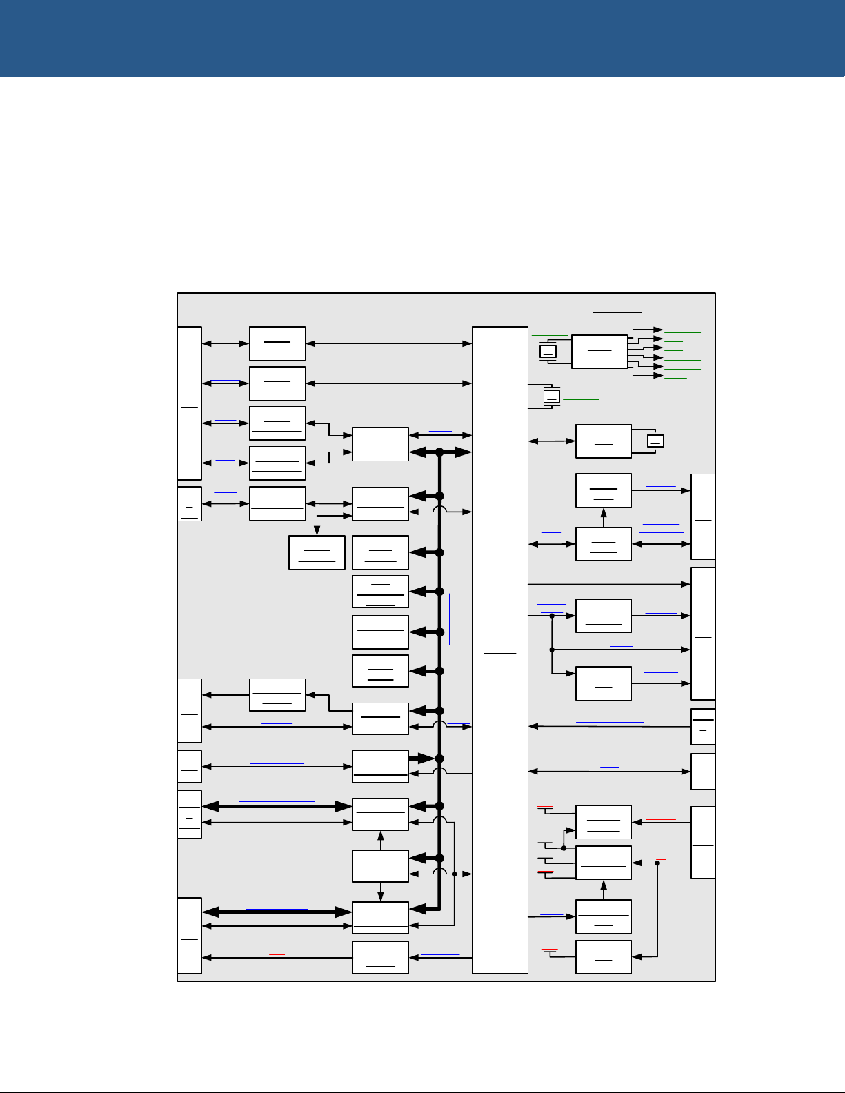
VIPER block diagram
The diagram below illustrates the functional organization of the VIPER PC/104 SBC.
PXA255
64MB
SDRAM
1MB
Bootloader
FLASH
16 or 32MB
Silicon Disk
256kB
SRAM
DUART
PL4
COM 1 RS232
Transceiver
RS232
Transceiver
COM 2&3
COM 4
COM5
RS232
Transceiver
RS422/485
Transceiver
PL5
CF Power
Switch
USB Power
Switch
Buffers and
Transceivers
CPLD
Buffers and
Transceivers
Address & Data
CF & PC/104 Control Signals
PC/104 Control
PC/104 Address & Data
CF Address & Data
CF Control
CF_SWITCH
PL11
&
PL12
LAN91C111
PL1
&
PL2
10/100
baseTX
Serial
EEPROM
Transformer
Buffers and
Transceivers
PL9 IN[0:7] / OUT[0:7]
USB Host
Controller
PL7
USB1 & 2
X2
Voltage
Monitor
Triple Reg
Reg
Micropower
DAC
JTAG
X3 Clock
Generation
RTC X1
PL6
AMP R+L
LINE IN R+L
LINE OUT R+L
MIC IN
AC'97
Codec
Power
Amp
AC'97
Signals
Dual
MOSFET
PL3
BLKEN &
LCDEN
LCD Signals
Reg
POSBIAS /
NEGBIAS
BLKSAFE &
LCDSAFE
LCDEN
VIPER
Control
Control
Control
Control
PL10
PL17
&
LK1
Control
PL16
Jumper Configuration
3.6864MHz
25MHz
14.318MHz 1.8432MHz
6MHz
8MHz
24.576MHz
14.318MHz
32.768kHz
3.3V 1.8V
3.3V
1.06-1.29V
3.3V
5V
VBAT_IN
3.3V
5V
© 2004 Arcom Issue H 13

VIPER Detailed hardware description
VIPER address map
PXA255
chip
select Physical address
Bus/register
width Description
- 0xA4000000 – 0xFFFFFFFF - Reserved
SDCS0 0xA0000000 – 0xA3FFFFFC 32-bit SDRAM, IC2&3
- 0x4C000000 – 0x9FFFFFFF - Reserved
NA 0x48000000 – 0x4BFFFFFF 32-bit Memory Control Registers 1
NA 0x44000000 – 0x47FFFFFF 32-bit LCD Control Registers 1
NA 0x40000000 – 0x43FFFFFF 32-bit PXA255 Peripherals 1
- 0x3C200400 – 0x3FFFFFFF - Reserved
NA 0x3C000000 – 0x3C1FFFFF 16-bit PC/104 Memory Space
- 0x30000400 – 0x3BFFFFFF - Reserved
NA 0x30000000 – 0x300003FF 16-bit PC/104 I/O Space
NA 0x20000000 – 0x2FFFFFFF 32-bit CompactFLASH, PL5
- 0x14840000 – 0x1FFFFFFF - Reserved
CS5 0x14800000 – 0x1483FFFF 8-bit SRAM (see page 24)
- 0x14500001 – 0x47FFFFFF - Reserved
CS5 0x14500000 – 0x14500000 8-bit General Purpose Input, PL9
(see page 66)
- 0x14300020 – 0x144FFFFF - Reserved
CS5 0x14300010 – 0x1430001F 8-bit COM4 (see page 46)
CS5 0x14300000 – 0x1430000F 8-bit COM5 (see page 46)
- 0x14100004 – 0x142FFFFF - Reserved
CS5 0x14100002 – 0x14100003 8-bit ICR Register (see page 26)
CS5 0x14100000 – 0x14100001 8-bit PC104I Register (see page 26)
- 0x10000004 – 0x140FFFFF - Reserved
CS4 0x10000000 – 0x10000002 32-bit Ethernet Data port
- 0x0C000004 – 0x0FFFFFFF - Reserved
CS3 0x0C000000 – 0x0C000002 16-bit USB Host Controller
- 0x08000310 – 0x0BFFFFFF - Reserved
CS2 0x08000300 – 0x0800030E 16-bit Ethernet I/O Space
- 0x06000000 – 0x080002FF - Reserved
CS1 0x04000000 – 0x05FFFFFE 16-bit FLASH Memory / Silicon Disk
- 0x00100000 – 0x03FFFFFF - Reserved
CS0 0x00000000 – 0x000FFFFE 16-bit Bootloader FLASH
1Details of the internal registers are in the Intel Developer Manual on the Development Kit CD.
© 2004 Arcom Issue H 14

VIPER Detailed hardware description
Translations made by the MMU
For details of translations made by the MMU by Redboot for embedded Linux, please
refer to VIPER embedded Linux Quickstart Manual.
For details of translations made by the MMU by Redboot for VxWorks, please refer to
VIPER VxWorks Quickstart and Technical Manual
For details of translations made by the MMU for Windows CE .NET, please check the
Windows CE .NET documentation for more information about memory mapping. One
source of this information is on the msdn website under Windows CE .NET Memory
Architecture.
© 2004 Arcom Issue H 15

VIPER Detailed hardware description
PXA255 processor
The PXA255 is a low power ARM (version 5TE) instruction set compliant RISC
processor. The PXA255 does not include a floating-point unit. The device does,
however, contain a DSP co-processor to enhance multimedia applications.
The 400MHz PXA255 is driven by a 3.6864 MHz clock, which generates all the high-
speed clocks within the device. The default run mode frequency is 400MHz for
embedded Linux, VxWorks and Windows CE .NET. Currently embedded Linux and
VxWorks supports changing the operating frequency and Windows CE .NET will
provide support shortly. Please refer to the relevant operating system technical manual
to select an alternative operating frequency.
The processor has two supply inputs: I/O and core generated on the VIPER from the
main +5V supply input. The I/O supply is powered from +3.3V, and the core is powered
from a +1.06 to +1.3V adjustable supply. See the section Processor power
management, page 55, for operation details.
The PXA255 has an integrated Memory and CompactFlash Controller with 100 MHz
Memory Bus, 32 KB data and 32 KB instruction caches and 2 KB Mini data cache for
streaming data.
The PXA255 provides up to 85 GPIO pins, many of these have been configured for
alternative functions like the AC’97 and PC card / CompactFLASH interfaces. Details of
these pin configurations are provided in the section PXA255 GPIO pin assignments,
page 17.
The PXA255 also has the following features that can be used on the VIPER:
Peripheral Control Module:•
•
- 16 channel configurable DMA controller.
- Integrated LCD controller with unique DMA for fast color screen support.
- Serial ports including AC’97, three UARTs, and enhanced USB end point
interface.
System Control Module:
- General-purpose interruptible I/O ports.
- Real-time clock.
- Watchdog.
- Interval timers.
- Power management controller.
- Interrupt controller.
- Reset controller.
- Two on-chip oscillators.
The PXA255 processor is packaged in a 256-pin PBGA, which is attached to the board
during the assembly process.
The PXA255 processor is a low power device and does not require a heat sink for
temperatures up to 70°C (85°C for the industrial variant).
© 2004 Arcom Issue H 16

VIPER Detailed hardware description
PXA255 GPIO pin assignments
The following table summarizes the use of the 85 PXA255 GPIO pins, their direction,
alternate function and active level.
For embedded Linux the GPIO pins are setup by Redboot. Under VxWorks and
Windows CE .NET, they are setup by themselves and not by the bootloader.
Key:
AF Alternate function.
Dir Pin direction.
Active Function active level or edge.
Sleep Pin state during sleep mode (all Hi-Z states are to ‘1’ during sleep).
GPIO
No AF Signal Name Dir Active Sleep Function See section…
0 0 ETHER_INT Input Input Ethernet Interrupt
1 0 PC/104_IRQ Input See
page 26
Input CPLD Interrupt
2 0 USB_IRQ Input Input USB Interrupt
3 0 UART_INT1 Input Input COM 5 Interrupt
4 0 UART_INT2 Input Input COM 4 Interrupt
Interrupt assignments
(page 25) and Wake up
events (page 58)
5 0
USER_CONFIG1 Input NA Input User Config 1, Jumper
LK2
User configurable jumper 1
– LK2 (page 70)
6 0 PSU_DATA Output NA 0 Microprocessor Core
Voltage DAC Data
Processor power
management (page 55)
7 0
Reserved Input NA Input Reserved Reserved – LK3 (page 70)
8 0 CF_RDY Input NA Input CompactFLASH
Ready/nBusy
Interrupt assignments,
(page 25 and
CompactFLASH
page 24)
9 0 BLKEN Output High 0 LCD Backlight Enable LCD backlight enable
(page 31)
10 0 LCDEN Output High 0 LCD Logic Supply
Enable
LCD logic supply enable
(page 32)
11 0 PSU_CLK Output 0 Microprocessor Core
Voltage DAC Clock
Processor power
management (page 55)
12 0 SHDN Output High 1 COM 1, 2, 3 & 4 UART
Shutdown
13 0 EN1# Output Low 0 COM 1, 2, 3 & 4 UART
Enable
UART power management
(page 57)
© 2004 Arcom Issue H 17
VIPER Detailed hardware description
GPIO
No AF
Signal Name Dir Active Sleep Function See section…
14 0 FLASH_
STATUS
Input NA Input Bootloader FLASH
Status,
Ready / nBusy
Interrupt assignments
(page 25) and FLASH
memory/silicon disk (page
23)
15 2 CS1 Output Low Hi-Z Chip Select 1 VIPER address map
(page 14)
16 2 PWM0 Output See
inverter
datasheet
0 Backlight Brightness
On/Off or variable if
PWM
LCD backlight brightness
control (page 32)
17 2 PWM1 Output NA 0 STN Bias STN BIAS voltage
(page 32)
18 1 ARDY Input Low Input 10/100 Ethernet PHY
Ready
-
19 0 PSU_nCS_LD Output Low 0 Microprocessor Core
Voltage DAC Chip
Select
Processor power
management (page 55)
20 0 OUT0
21 0 OUT1
22 0 OUT2
23 0 OUT3
24 0 OUT4
25 0 OUT5
26 0 OUT6
27 0 OUT7
Output User
Config 0 User Config General purpose I/O
(page 39)
28 1 AC97_BITCLK Input Input BITCLK
29 1 AC97_IN Input NA Input SDATA_IN0
30 2 AC97_OUT Output NA 0 SDATA_OUT
31 2 AC97_SYNC Output 0 SYNC
-
32 0 CF_DETECT Input Input CF Detection Interrupt assignments
(page 25) and
CompactFLASH (page 24)
33 2 CPLDCS Output Low Hi-Z Chip Select 5 VIPER address map,
(page 14)
© 2004 Arcom Issue H 18

VIPER Detailed hardware description
GPIO
No AF
Signal Name Dir Active Sleep Function See section…
34 1 RXD1 Input NA Input COM1 Receive Data
35 1 CTS1 Input NA Input COM1 Clear To Send
36 1 DCD1 Input NA Input COM1 Data Carrier
Detect
37 1 DSR1 Input NA Input COM1 Data Sender
Ready
38 1 RI1 Input NA Input COM1 Ring Indicator
39 2 TXD1 Output NA 0 COM1 Transmit Data
40 2 DTR1 Output NA 0 COM1 Data Terminal
Ready
41 2 RTS1 Output NA 0 COM1 Request To
Send
42 1 RXD2 Input NA Input COM2 Receive Data
43 2 TXD2 Output NA 0 COM2 Transmit Data
44 1 CTS2 Input NA Input COM2 Clear To Send
45 2 RTS2 Output NA 0 COM2 Request To
Send
46 2 RXD3 Input NA Input COM3 Receive Data
47 1 TXD3 Output NA 0 COM3 Transmit Data
Serial COMs ports
(page 45) and PL4 –
COMS ports (page 63).
48 2 CB_POE Output Low Hi-Z Socket 0 & 1 Output
Enable
49 2 CB_PWE Output Low Hi-Z Socket 0 & 1 Write
Enable
50 2 CB_PIOR Output Low Hi-Z Socket 0 & 1 I/O Read
51 2 CB_PIOW Output Low Hi-Z Socket 0 & 1 I/O Write
52 2 CB_PCE1 Output Low Hi-Z Socket 0 & 1 Low Byte
Enable
53 2 CB_PCE2 Output Low Hi-Z Socket 0 & 1 High
Byte Enable
-
54 2 CB_PKTSEL Output NA 0 PSKTSEL 0 = Socket
0 Select / 1 = Socket 1
Select
-
55 2 CB_PREG Output Low 0 PREG -
56 1 CB_PWAIT Input Low Input PWAIT
57 1 CB_PIOIS16 Input Low Input IOIS16
-
© 2004 Arcom Issue H 19

VIPER Detailed hardware description
GPIO
No AF
Signal Name Dir Active Sleep Function See section…
58 2 LCD_D0 Output NA 0 LCD Data Bit 0
59 2 LCD_D1 Output NA 0 LCD Data Bit 1
60 2 LCD_D2 Output NA 0 LCD Data Bit 2
61 2 LCD_D3 Output NA 0 LCD Data Bit 3
62 2 LCD_D4 Output NA 0 LCD Data Bit 4
63 2 LCD_D5 Output NA 0 LCD Data Bit 5
64 2 LCD_D6 Output NA 0 LCD Data Bit 6
65 2 LCD_D7 Output NA 0 LCD Data Bit 7
66 2 LCD_D8 Output NA 0 LCD Data Bit 8
67 2 LCD_D9 Output NA 0 LCD Data Bit 9
68 2 LCD_D10 Output NA 0 LCD Data Bit 10
69 2 LCD_D11 Output NA 0 LCD Data Bit 11
70 2 LCD_D12 Output NA 0 LCD Data Bit 12
71 2 LCD_D13 Output NA 0 LCD Data Bit 13
72 2 LCD_D14 Output NA 0 LCD Data Bit 14
73 2 LCD_D15 Output NA 0 LCD Data Bit 15
74 2 LCD_FCLK Output NA 0 LCD Frame Clock (STN)
Vertical Sync (TFT)
75 2 LCD_LCLK Output NA 0 LCD Line Clock (STN) /
Horizontal Sync (TFT)
76 2 LCD_PCLK Output NA 0 LCD Pixel Clock
(STN) / Clock (TFT)
77 2 LCD_BIAS Output NA 0 LCD Bias (STN) / Date
Enable (TFT)
Flat panel display support
(page 29) and PL3 – LCD
connector (page 62)
78 2 ETHERCS2 Output Low Hi-Z Chip Select 2
79 2 USBCS Output Low Hi-Z Chip Select 3
80 2 ETHERCS1 Output Low Hi-Z Chip Select 4
VIPER address map (page
14)
81 0 SDRAM Input NA Input SDRAM Size
Detection 0 = 64MB,
1 = 16MB
-
82 0 CF_SWITCH Output High 0 CompactFLASH
Power Switch Enable
CompactFLASH (page 24)
and CompactFLASH
power management
(page 57)
83 0 RTC_IO Bidirec-
tional
NA 0 RTC Data
84 0 RTC_CLK Output 0 RTC Clock
Real Time Clock (page 21)
© 2004 Arcom Issue H 20
Table of contents
Other Arcom Motherboard manuals


