austriamicrosystems AS3990 User manual

AS3990/AS3991
UHF RFID Single Chip Reader EPC Class1 Gen2 Compatible
www.austriamicrosystems.com/AS3990
www.austriamicrosystems.com/AS3991 Revision 3.9 1 - 51
Datasheet
1 General Description
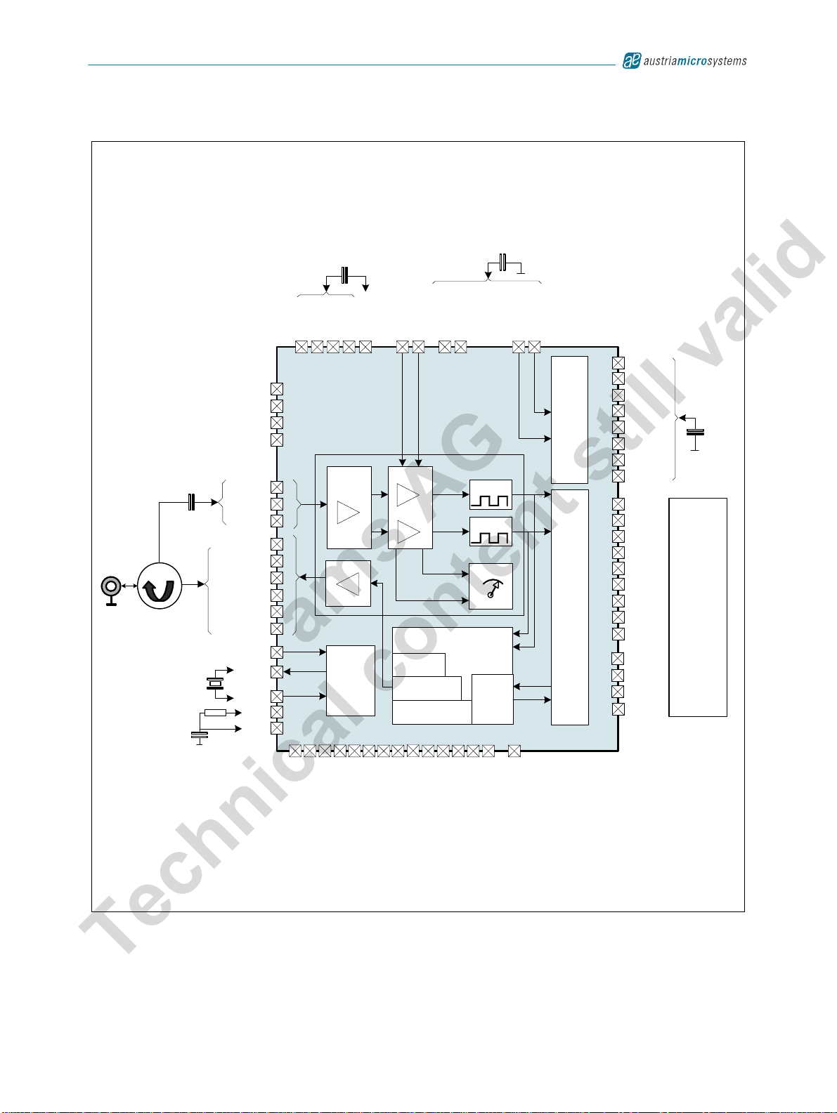
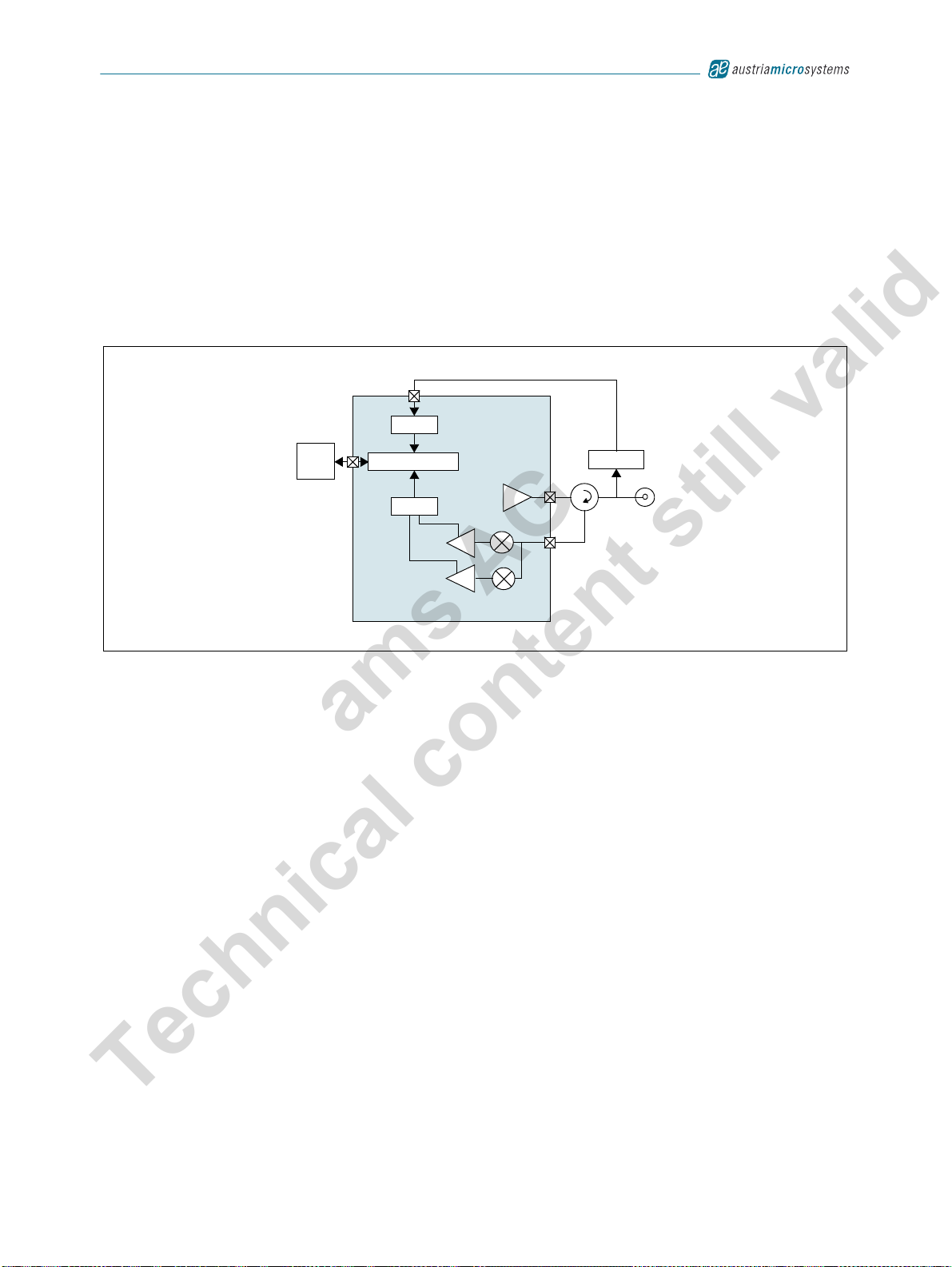
The AS3990/AS3991 UHF reader chip is an integrated analog front
end and protocol handling systems for a ISO18000-6C 900MHz
RFID reader system.
Equippedwithbuilt-inprogrammingoptions,thedeviceissuitablefor
a wide range of UHF RFID applications. The AS3990/AS3991
includes improved on-board VCO and internal PA.
The reader configuration is achieved by selecting the desired
protocol in control registers. Direct access to all control registers
allows fine tuning of different reader parameters.
Parallel or serial interface can be selected for communication
between the host system (MCU) and the reader IC. When hardware
coders and decoders are used for transmission and reception, data
is transferred via 24 bytes FIFO register.
In case of direct transmission or reception, coders and decoders are
bypassed and the host system can service the analog front end in
real time.
Thetransmitter generates20dBmoutput power into50Ωload and is
capable of ASK or PR-ASK modulation. The integrated supply
voltage regulators ensure supply rejection of the complete reader
system.
Thetransmissionsystemcompriseslowleveldatacoding.Automatic
generation of FrameSync, Preamble, and CRC is supported.
The receiver system allows AM and PM demodulation. The receiver
also comprises automatic gain control option (patent pending) and
selectable gain and signal bandwidth to cover a range of input link
frequency and bit rate options.
The signal strength of AM and PM modulation is measured and can
be accessed in RSSI register.
Thereceiveroutputis selectablebetweendigitized sub-carriersignal
and any of integrated sub-carrier decoders. Selected decoders
deliver bit stream and data clock as outputs.
The receiver system also comprises framing system. This system
performs the CRC check and organizes the data in bytes. Framed
data is accessible to the host system through a 24 byte FIFO
register.
To support external MCU and other circuitry a 3.3V regulated supply
and clock outputs are available. The regulated supply has 20mA
current capability.
The AS3990/AS3991 is available in a 64-pin QFN (9mm x 9mm),
ensuring the smallest possible footprint.
2 Key Features
Filters dedicated to 250kHz and 320kHz M4 and M8 DRM
operation. Available RX modes:
- LF40kHz, 160kHz: FM0, M2, M4, M8
- LF 250kHz, 320kHz, 640kHz: M4, M8
ISO18000-6C (EPC Gen2) full protocol support
ISO18000-6A,B compatibility in direct mode
Integrated low level transmission coding
Integrated low level decoders
Integrated data framing
Integrated CRC checking
Parallel 8-bit or serial4-pinSPIinterface to MCU using24bytes
FIFO
Voltage range for communication to MCU between 1.8V and
5.5V
Selectable clock output for MCU
Integrated supply voltage regulator (20mA), which can be used
to supply MCU and other external circuitry
Integrated supply voltage regulator for the RF output stage,
providing rejection to supply noise
Internal power amplifier (20dBm) for short range applications
Modulator using ASK or PR-ASK modulation
Adjustable ASK modulation index
AM & PM demodulation ensuring no“communication holes”
with automatic I/Q selection
Built-in reception low-pass and high-pass filters having select-
able corner frequencies
Selectable reception gain
Reception automatic gain control
AD converter for measuring TX power using external RF power
detector
DA converter for controlling external power amplifier
Frequency hopping support
On-board VCO and PLL covering complete RFID frequency
range 840MHz to 960MHz
Oscillator using 20MHz crystal
Power down, standby and active mode
Can be powered by USB with no need for step conversion
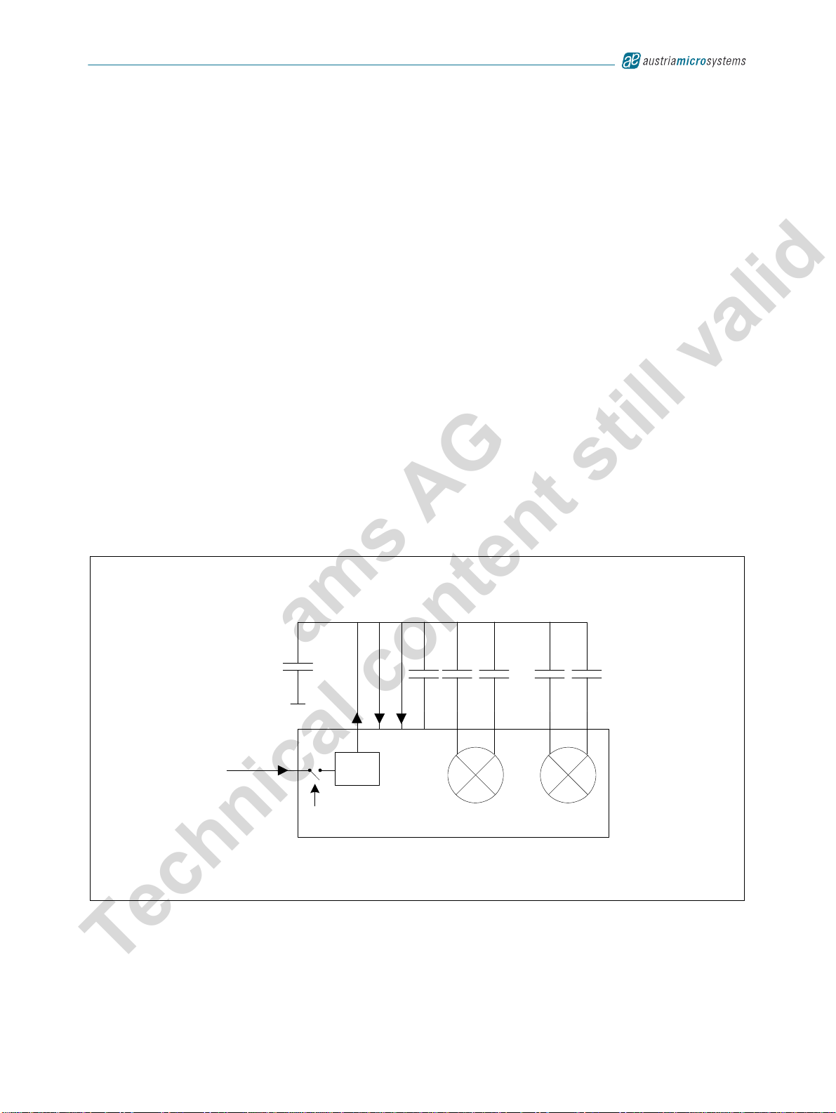
3 Applications
The device is an ideal solution for UHF RFID reader systems and
hand-held UHF RFID readers.
ams AG
Technical content still valid

www.austriamicrosystems.com/AS3990
www.austriamicrosystems.com/AS3991 Revision 3.9 2 - 51
AS3990/AS3991
Datasheet - Applications
Figure 1. Block Diagram
MCU Interface
AS3990 /
AS3991
Directional unit
COMN_A
COMP_B
COMN_B
VDD_5LFI
VSS
VSS
MIX_INP
MIX_INN
MIXS_IN
VSN_MIX
CBIB
VDD_MIX
CBV5
VDD_TXPAB
VEXT
VEXT2
RFOUTN_2
RFOUTN_1
RFOUTP_2
RFOUTP_1
VSN_1
VSN_2
VSN_3
VSN_4
VSN_5
VSN_D
RFOPX
RFONX
VSN_RFP
OSCO
OSCI EN
IRQ
IO0
IO1
IO2
IO3
IO4
IO5
IO6
IO7
CLSYS
CLK
VDD_IO
VDD_D
VDD_RF
VDD_B
AGD
VSN_A
EXT_IN
VSN_CP
VDD_A
VDDLF
COMP_A
EXP_PAD
CD1
CD2
VDD_RFP
4xC 2xC
7xC
Micro
controller
Oscillator
& Timing
System
RSSI
AFE
Digitizer
Digitizer
IQ Down-
Conversion
Mixer
Gain Filter
RF Out
24 Byte
FIFO
EPC Gen2 Protocol
Handling
CRC
GEN-2
Frame Gen
OAD
OAD_2
ADC
DAC
VCO
CP
Supply Regulators &
References
31
30
58
4
7
9
10
27
28
20
21
32
33
56
36
37
60
6268111214222324
25 26 29 35 55 57 65
49
40
39
50
48
47
46
45
44
43
42
41
51
VOSC
34
61
63
59
54
19
18
38
64 2 1 3 5 53 52 13 15 16 17
ams AG
Technical content still valid

www.austriamicrosystems.com/AS3990
www.austriamicrosystems.com/AS3991 Revision 3.9 3 - 51
AS3990/AS3991
Datasheet - Contents
Contents
1 General Description.................................................................................................................................................................. 1
2 Key Features............................................................................................................................................................................. 1
3 Applications............................................................................................................................................................................... 1
4 Pin Assignments....................................................................................................................................................................... 5
4.1 Pin Descriptions.................................................................................................................................................................................... 5
5 Absolute Maximum Ratings...................................................................................................................................................... 8
6 Electrical Characteristics........................................................................................................................................................... 9
7 Detailed Description................................................................................................................................................................ 11
7.1 Supply................................................................................................................................................................................................. 11
7.1.1 Power Modes............................................................................................................................................................................. 12
7.2 Host Communication.......................................................................................................................................................................... 12
7.3 VCO and PLL ..................................................................................................................................................................................... 13
7.3.1 VCO and External RF Source.................................................................................................................................................... 13
7.3.2 PLL ............................................................................................................................................................................................ 13
7.4 Chip Status Control ............................................................................................................................................................................ 13
7.5 Protocol Control.................................................................................................................................................................................. 13
7.6 Option Registers Preset ..................................................................................................................................................................... 14
7.7 Transmitter.......................................................................................................................................................................................... 14
7.7.1 Normal Mode............................................................................................................................................................................. 14
7.7.2 Direct Mode ............................................................................................................................................................................... 16
7.7.3 Modulator................................................................................................................................................................................... 16
7.7.4 Amplifier..................................................................................................................................................................................... 17
7.8 Receiver............................................................................................................................................................................................. 17
7.8.1 Input Mixer................................................................................................................................................................................. 17
7.8.2 RX Filter..................................................................................................................................................................................... 17
7.8.3 RX Gain..................................................................................................................................................................................... 18
7.8.4 Received Signal Strength Indicator (RSSI)................................................................................................................................ 18
7.8.5 Reflected RF Level Indicator ..................................................................................................................................................... 18
7.8.6 Normal Mode............................................................................................................................................................................. 18
7.8.7 Direct Mode ............................................................................................................................................................................... 19
7.8.8 Normal Mode With Mixer DC Level Output And Enable RX Output Available........................................................................... 20
7.9 ADC / DAC ......................................................................................................................................................................................... 20
7.9.1 DA Converter............................................................................................................................................................................. 20
7.9.2 AD Converter............................................................................................................................................................................. 20
7.10 Reference Oscillator......................................................................................................................................................................... 20
8 Application Information........................................................................................................................................................... 21
8.1 Configuration Registers Address Space............................................................................................................................................. 21
8.2 Main Configuration Registers............................................................................................................................................................. 22
8.3 Control Registers - Low Level Configuration Registers...................................................................................................................... 23
8.4 Status Registers................................................................................................................................................................................. 28
8.5 Test Registers..................................................................................................................................................................................... 31
8.6 PLL, Modulator, DAC, and ADC Registers......................................................................................................................................... 32
8.7 RX Length Registers .......................................................................................................................................................................... 35
8.8 FIFO Control Registers....................................................................................................................................................................... 36
8.9 Direct Commands............................................................................................................................................................................... 37
ams AG
Technical content still valid

www.austriamicrosystems.com/AS3990
www.austriamicrosystems.com/AS3991 Revision 3.9 4 - 51
AS3990/AS3991
Datasheet - Contents
8.9.1 Idle (80)...................................................................................................................................................................................... 38
8.9.2 Soft Init (83)............................................................................................................................................................................... 38
8.9.3 Hop to Main Frequency (84)...................................................................................................................................................... 38
8.9.4 Hop to Auxiliary Frequency (85)................................................................................................................................................ 38
8.9.5 Trigger AD Conversion (87)....................................................................................................................................................... 38
8.9.6 Reset FIFO (8F)......................................................................................................................................................................... 38
8.9.7 Transmission With CRC (90)..................................................................................................................................................... 38
8.9.8 Transmission With CRC Expecting Header Bit (91).................................................................................................................. 38
8.9.9 Transmission Without CRC (92)................................................................................................................................................ 38
8.9.10 Delayed Transmission With CRC (93)..................................................................................................................................... 39
8.9.11 Delayed Transmission Without CRC (94)................................................................................................................................ 39
8.9.12 Block RX (96)........................................................................................................................................................................... 39
8.9.13 Enable RX (97)........................................................................................................................................................................ 39
8.10 EPC GEN2 Specific Commands ...................................................................................................................................................... 39
8.10.1 Query (98)................................................................................................................................................................................ 39
8.10.2 QueryRep (99)......................................................................................................................................................................... 39
8.10.3 QueryAdjustUp (9A)................................................................................................................................................................. 39
8.10.4 QueryAdjustNic (9B)................................................................................................................................................................ 39
8.10.5 QueryAdjustDown (9C)............................................................................................................................................................ 39
8.10.6 ACK (9D) ................................................................................................................................................................................. 39
8.10.7 NAK (9E).................................................................................................................................................................................. 39
8.10.8 ReqRN (9F) ............................................................................................................................................................................. 40
8.11 Reader Communication Interface..................................................................................................................................................... 40
8.12 Parallel Interface Communication..................................................................................................................................................... 42
8.13 Serial Interface Communication ....................................................................................................................................................... 43
8.13.1 Timing Diagrams...................................................................................................................................................................... 44
8.13.2 Timing Parameters .................................................................................................................................................................. 45
8.14 FIFO................................................................................................................................................................................................. 45
9 Package Drawings and Markings ........................................................................................................................................... 46
10 Ordering Information............................................................................................................................................................. 50
ams AG
Technical content still valid

www.austriamicrosystems.com/AS3990
www.austriamicrosystems.com/AS3991 Revision 3.9 5 - 51
AS3990/AS3991
Datasheet - Pin Assignments
4 Pin Assignments
Figure 2. Pin Assignments (Top View)
4.1 Pin Descriptions
Table 1. Pin Descriptions
Pin Number Pin Name Pin Type Description
1COMN_A
Bidirectional Connect de-coupling capacitor to VDD_5LFI
2COMP_B
3COMN_B
4 DAC Output DAC output for external amplifier support, Output Resistance of DAC pin
is 1kΩ
5 VDD_5LFI Supply Input Positive supply for LF input stage, connect to VDD_MIX
6 VSS Substrate
7 MIX_INP Input Differential mixer positive input
8 VSS Supply Input Substrate
9MIX_INN Input Differential mixer negative input
10 MIXS_IN Single ended mixer input
1
2
3
4
5
6
7
8
9
10
11
12
13
14
15
16
39
38
37
36
35
34
33
46
45
44
43
42
41
40
48
47
28
29
30
31
32
23
24
25
26
27
18
19
20
21
22
17
53
52
51
50
49
58
57
56
55
54
63
62
61
60
59
64
AS3990/AS3991
RFOUTN_2
VSN_D
OAD2
OAD
RFONX
VSN_2
VSN_3
VSN_4
VSN_5
RFOUTN_1
VDD_RF
VDD_B
RFOUTP_1
RFOUTP_2
VSN_1
VEXT2
CD1
CD2
VDD_IO
CLK
CLSYS
ADC
VSN_CP
EXT_IN
VSN_A
AGD
VDDLF
CP
VOSC
VCO
VDD_A
COMP_A
EN
VDD_D
OSCO
OSCI
VSN_RFP
VDD_RFP
RFOPX
IO5
IO4
IO3
IO2
IO1
IO0
IRQ
IO7
IO6
COMN_A
COMP_B
COMN_B
DAC
VDD_5LFI
VSS
MIX_INP
VSS
MIX_INN
MIXS_IN
VSN_MIX
CBIB
VDD_MIX
CBV5
VDD_TXPAB
VEXT
ams AG
Technical content still valid

www.austriamicrosystems.com/AS3990
www.austriamicrosystems.com/AS3991 Revision 3.9 6 - 51
AS3990/AS3991
Datasheet - Pin Assignments
11 VSN_MIX Supply Input Mixer negative supply
12 CBIB Bidirectional Internal node de-coupling capacitor to GND
13 VDD_MIX Supply Output Mixer positive supply, internally regulated to 4.8V
14 CBV5 Bidirectional Internal node de-coupling capacitor to VDD_MIX
15 VDD_TXPAB
Supply Input
Power Amplifier Bias positive supply. Connect to VDD_MIX
16 VEXT Main positive supply input (5…5.5V)
17 VEXT2 PA positive supply regulator input (2.5… 5.5V)
18 VDD_RF Supply Output PA positive supply regulator output, internally regulated to 2…3.5V
19 VDD_B PA buffer positive supply. Internally regulated to 3.4V
201RFOUTP_1 Output PA positive RF output
RFOUT1 and RFOUT2 must be tied together
211RFOUTP_2
221VSN_1
Supply Input PA negative supply
231VSN_2
241VSN_3
251VSN_4
261VSN_5
271RFOUTN_1 Output PA negative RF output or used in single ended mode.
RFOUT1 and RFOUT2 must be tied together
281RFOUTN_2
29 VSN_D Supply Output Digital negative supply
30 OAD2 Bidirectional Analog or digital received signal output and MCU support mode sense
input
31 OAD Analog or digital received signal output
32 RFONX Output Low power linear negative RF output (~0dBm)
33 RFOPX Low power linear positive RF output (~0dBm)
34 VDD_RFP Supply Output RF path positive supply, internally regulated to 3.4V
35 VSN_RFP Supply Input RF path negative supply
36 OSCI Input Crystal oscillator input
37 OSCO Bidirectional Crystal oscillator output or external 20MHz clock input
38 VDD_D Supply Output Digital part positive supply, internally regulated to 3.4V
39 EN Input Enable input
40 IRQ Output Interrupt output
Table 1. Pin Descriptions
Pin Number Pin Name Pin Type Description
ams AG
Technical content still valid

www.austriamicrosystems.com/AS3990
www.austriamicrosystems.com/AS3991 Revision 3.9 7 - 51
AS3990/AS3991
Datasheet - Pin Assignments
41 IO0
Bidirectional
I/O pin for parallel communication
42 IO1
43 IO2 I/O pin for parallel communication
EnableRX input in case of direct mode
44 IO3 I/O pin for parallel communication
Modulation input in case of direct mode
45 IO4 I/O pin for parallel communication
Slave select in case of serial communication (SPI)
46 IO5 I/O pin for parallel communication
Sub-carrier output in case of direct mode
47 IO6 Bidirectional
I/O pin for parallel communication.
MISO in case of serial communication (SPI)
Sub-carrier output in case of direct mode
48 IO7 I/O pin for parallel communication.
MOSI in case of serial communication (SPI)
49 CLSYS Output Clock output for MCU operation
50 CLK Input Clock input for MCU communication (parallel and serial)
51 VDD_IO Supply Input Positive supply for peripheral communication, connect to host positive
supply
52 CD2 Bidirectional Internal node de-coupling capacitor
53 CD1 Bidirectional
54 AGD Analog reference voltage
55 VSN_A Supply Input Analog part negative supply
56 EXT_IN Input RF input in case external VCO is used
57 VSN_CP Supply Input Charge pump negative supply
58 ADC Input ADC input for external power detector support
59 VDD_A Supply Output Analog part positive supply, internally regulated to 3.4V
60 VCO Input VCO input
61 VOSC Bidirectional Internal node de-coupling capacitor
62 CP Output Charge pump output
63 VDDLF Supply Input Positive supply for LF processing, internally regulated to 3.4V
64 COMP_A Bidirectional Internal node, connect de-coupling capacitor to VDD_5LFI
65 EXP_PAD Supply Input Exposed paddle, must be tied to GND
1. Internal Power amplifier is not available on AS3990.
Table 1. Pin Descriptions
Pin Number Pin Name Pin Type Description
ams AG
Technical content still valid

www.austriamicrosystems.com/AS3990
www.austriamicrosystems.com/AS3991 Revision 3.9 8 - 51
AS3990/AS3991
Datasheet - Absolute Maximum Ratings
5 Absolute Maximum Ratings
Stresses beyond those listed in Table 2 may cause permanent damage to the device. These are stress ratings only, and functional operation of
the device at these or any other conditions beyond those indicated in Electrical Characteristics on page 9 is not implied. Exposure to absolute
maximum rating conditions for extended periods may affect device reliability.
Table 2. Absolute Maximum Ratings
Parameter Min Max Units Comments
Electrical Parameters
Supply voltage, VEXT 5.5 V -
Positive voltage other pads VS± 0.3 V-
Negative voltage other pads -0.3 V -
Output current, IO±100 mA -
Electrostatic Discharge
ESD rating1
1. This integrated circuit can be damaged by ESD. We recommend that all integrated circuits are handled with appropriate precautions.
Failure to observe proper handling and installation procedures can cause damage. ESD damage can range from subtle performance
degradation to complete device failure. Precision integrated circuits may be more susceptible to damage because very small parametric
changes could cause the device not to meet the published specifications. RF integrated circuits are also more susceptible to damage
due to use of smaller protection devices on the RF pins, which are needed for low capacitive load on these pins.
IO pins, HBM 2 kV According to MIL 883 Emethod 3015
RF pins, HBM 1 kV
Temperature Ranges and Storage Conditions
Maximum junction temperature, TJ125 ºC The maximum junction temperature for continuous
operation is limited by package constraints.
Storage temperature range, Tstg -55 +150 ºC -
Lead temperature 1.6 mm (1/16 inch) from case
for 10 seconds 260 ºC
The reflow peak soldering temperature (body
temperature) specified is in accordance with IPC/
JEDEC J-STD-020 “Moisture/Reflow Sensitivity
Classification for Non-Hermetic Solid State Surface
Mount Devices”.
Thelead finish forPb-free leaded packages ismatte tin
(100% Sn)
ams AG
Technical content still valid

www.austriamicrosystems.com/AS3990
www.austriamicrosystems.com/AS3991 Revision 3.9 9 - 51
AS3990/AS3991
Datasheet - Electrical Characteristics
6 Electrical Characteristics
VEXT = 5.3V, typical values at 25ºC, unless otherwise noted.
Table 3. Electrical Characteristics
Symbol Parameter Conditions Min Typ Max Units
IVEXT Supply current without PA driver
current VEXT Consumption 80 mA
IVEXT+IVEXT2 Supply Current for AS3991 and
internal PA1
1. Internal PA is available on AS3991only.
VEXT2 Consumption,
VEXT2 = 2.5V 310 mA
ISTBY Standby current - 3 mA
IPD Supply current in power-down mode All system disabled including supply
voltage regulators 20 100 µA
210
VAGD AGD voltage - 1.5 1.6 1.7 V
VPOR Power on reset voltage (POR) - 1.4 2.0 2.5 V
VVDD Regulated supply for internal circuitry
and for external MCU - 3.2 3.4 3.6 V
VDD RF Regulated supply for internal PA - 1.9 2 2.1 V
VVDD MIX1 Regulated supply for mixers,
bit vext_low=L The difference between the external
supplyand the regulatedvoltage is higher
than 250mV
4.5 4.8 5.1 V
VVDD MIX2 Regulated supply for mixers,
bit vext_low=H 3.5 3.7 3.9 V
PPSSR Rejection of external supply noise on
the supply regulators 26 dB
PRFAUX Auxiliary output power - 0 dBm
PRFOUT Internal PA output power1-20dBm
RRFIN RFIN input resistance - 100 Ω
VSENS Input sensitivity - -66 dBm
1dBCP Input 1dB compression point - 10 dBm
IP3 Third order intercept point - 21 dBm
TREC Recovery time after modulation Maximum LF selected 10 µs
Logic Input / Output
- Maximum CLK frequency - 1 MHz
VLOW Input logic low - 0.2 VDD_IO
VHIGH Input logic high - 0.8 VDD_IO
RIO Output resistance IO0…IO7 low_io = H for VDD_IO < 2.7V 400 800 Ω
RCL SYS Output resistance CL SYS 200 Ω
ams AG
Technical content still valid

www.austriamicrosystems.com/AS3990
www.austriamicrosystems.com/AS3991 Revision 3.9 10 - 51
AS3990/AS3991
Datasheet - Electrical Characteristics
Table 4. Recommended Operating Conditions
Symbol Parameter Conditions Min Typ Max Units
- Supply Voltage - 5.0 5.3 5.5 V
- Supply voltage (bit vext_low set) - 4.1 V
TJOperating virtual junctiontemperature
range - -40 125 ºC
TAMB Ambient temperature - -40 85 ºC
- Rth junction to exposed die pad - 19 º/W
ams AG
Technical content still valid

www.austriamicrosystems.com/AS3990
www.austriamicrosystems.com/AS3991 Revision 3.9 11 - 51
AS3990/AS3991
Datasheet - Detailed Description
7 Detailed Description
The RFID reader IC comprises complete analog and digital functionality for reader operation including transmitter and receiver section with
complete EPC Gen2 or ISO18000-6C digital protocol support. To integrate as many components as possible, the device also comprises an on-
board PLL section with integrated VCO, supply section, DAC and ADC section, and host interface section. In order to cover a wide range of
possibilities, there is also Configuration registers section that configures operation of all blocks.
For operation, the device needs to be correctly supplied via. VEXT and VEXT2 pins and enabled via. EN pin (Refer Supply on page 11 for
connecting to supplyandPowerModes on page12about operationoftheENpin).Atpower-up theconfigurationregisters are preset to adefault
operation mode. The preset values are described in the Configuration Registers Address Space on page 21 below each register description
table. It is possible to access and change registers to choose other options.
The communication between the reader and the transponder follows the reader talk first method. After power-up and configuring IC, the host
system starts communication by turning on the RF field by setting option bit rf_on in the ‘Chip status control register’ (00) (see Table 13) and
transmitting the first protocol command (Select in EPC Gen2). Transmitting and receiving is possible in the following two modes:
1. Normal Data Mode: In this mode, the TX and RX data is transferred through the FIFO register and all protocol data processing is done
internally.
2. Direct Data Mode: In this mode, the data processing is done by the host system.
7.1 Supply
The effective supply system of the chip decreases the influence of the supply noise and interference and thus improves de-coupling between
different building blocks. A set of 3.4V regulators is used for supplying the reference block, AD and DA converters, low frequency receiver cells,
the RF part, and digital part. It is possible to use the digital part supply VDD_D for supplying the external MCU with a current consumption up to
20mA. The input pin for the regulators is VEXT. The output pins for regulators are VDD_A, VDD_LF, VDD_D, VDD_RFP and VDD_B. Each of
the pins require stabilizing capacitors to connected ground (2.2…10µF and 10…100nF) in parallel. Depending on quality of the capacitors,
100pF could be required.
Figure 3. Mixer Supply
An additional 4.8V regulator is used for the input RF mixers supply. The input of this regulator is VEXT, output is VDD_MIX pin. For correct
operation of the 4.8V regulator, the VEXT voltage needs to bebetween 5.3V and 5.5V. VDD_MIX needs de-couplingcapacitors to VDD_MIX like
other VDD pins.
In case lower VEXT supply voltage is used (down to 4.1V), two option bits have to be set to optimize the chip performance to the lower supply.
Thevext_low in the‘TRcalhigh and miscregister’(05) bit decreases VDD_MIXvoltage to 3.7V to maintain the regulators PSSRandtheir<1>bit
in the ‘RX special setting 2’ (0A) adapts mixer’s internal operating point to lower supply. Adaptation to low supply is implemented in differential
mixer only. The consequence of the decreased supply is lower mixer’s input range.
VDD_MIX
VDD_5LFI
VDD_TXPAB
CBV5
COMP_A
COMP_B
COMN_A
COMN_B
Mixer
LDO
VEXT
On
receive
ams AG
Technical content still valid

www.austriamicrosystems.com/AS3990
www.austriamicrosystems.com/AS3991 Revision 3.9 12 - 51
AS3990/AS3991
Datasheet - Detailed Description
VDD_5LFI and VDD_TXPAB pins are supply input pins and should be connected to VDD_MIX. The internal 20dBm power amplifier1has an
internal regulator from 2…3.5V. The output voltage selection is done by reg2v1:0 option bits in the ‘Regulator and IO control register’ (0B) (see
Table 24).
The input pin is VEXT2 and output is VDD_RF. For optimum noise rejection performance, the input voltage at VEXT2 pin needs to be at least
0.5V above the regulated supply output. Connecting VEXT2 directly to VEXTis possible only at the expense of increasing IC’spower dissipation
and decreasing the maximum operating temperature.
A separate I/O supply pin (VDD_IO) is used to supply the internal level shifters for communication interface to the host system (MCU). VDD_IO
should be connected to MCU supply to ensure proper communication between the chip and MCU. In case the MCU is supplied by VDD_D from
the reader IC also VDD_IO should be connected to VDD_D.
7.1.1 Power Modes
The chip has three power modes.
Power Down Mode: The power down mode is activated by EN pin low (EN=L). For correct operation, the OAD2 pin should not be con-
nected.
Normal Mode: The normal mode is entered by EN=H. In this case all supply regulators, reference voltage system, crystal oscillator, RF
oscillator and PLL are enabled. After the crystal oscillator stabilizes, the CLSYS clock becomes active (default frequency is 5MHz) and the
chip is ready to move to transmit or receive operation.
Standby Mode: The standby mode is entered from normal mode by option bit stby=H. In the standby mode the regulators, reference volt-
age system, and crystal oscillator are operating in low power mode; but the PLL, transmitter output stages and receiver are switched off. All
the register settings are kept while switching between standby and normal mode.
Power Down with MCU Support mode intends to support the MCU if the majority of the reader IC is in power down. This mode is enabled by
connecting 10kΩresistor between OAD2 pin and ground. During EN=L period, the VDD_D regulator is enabled in low power mode and the
CLSYS frequency is 60kHz typically.
It is also possible to trigger temporary normal mode from power down mode (EN=L) by pulling shortly the OAD2 pin low via 10kΩor less. After
the crystal oscillator is stable and the CLSYS clock output is active, the chip waits for approximately 200µs and then changes back to the power
down mode. Using this function, the superior system can wake up the reader IC and MCU that are both in the power down mode. If the MCU
during 200µs period finds out that the RFID system must react, it confirms the normal mode by setting EN high.
7.2 Host Communication
An8-bitparallel interface (pinsIO0toIO7)withtwocontrolsignals(CLK,IRQ)formsthemain communicationsystem. It can alsobechanged (by
hardwiring some of the 8 I/Opins) to a serial interface. The data handling is done bya24byteFIFOregister usedinbothdirections, transmission
and reception. For more details, refer Reader Communication Interface on page 40.
The signal level for communication between the host system (MCU) is defined by the supply voltage connected to VDD_IO pin. Communication
is possible in wide range between 1.8V and 5.5V. In case the pull-up output resistance at VDD_IO below 2.7V is to high, it can be decreased by
setting option bit vdd_io_low in the ‘TRcal High and Misc register’ (05). In case the MCU is supplied from the reader IC, then both the MCU
supply and VDD_IO pin need to be connected to VDD_D.
CLSYS output level is defined by the VDD_IO voltage. It is also possible to configure CLSYS to open drain N-MOS output by setting the option
bit open_dr in the in the ‘TRcal high and misc register’ (05), (see Table 18). This function can be used to decrease amplitude and harmonic
content of the CLSYS signal and decrease the cross-talk effects that could corrupt operation of other parts of the circuit.
1. Internal PA is available on AS3991only.
Table 5. AS3990/AS3991 Power Modes
Power Mode EN OAD2 Std by
Power down L - X
Power down
SYSCLK of 60kHz L 10k to GND X
Normal power H X X
Standby - X H
Listen mode L 10k and falling edge X
ams AG
Technical content still valid

www.austriamicrosystems.com/AS3990
www.austriamicrosystems.com/AS3991 Revision 3.9 13 - 51
AS3990/AS3991
Datasheet - Detailed Description
7.3 VCO and PLL
The PLL section is composed of a voltage control oscillator (VCO), prescaler, main and reference divider, phase-frequency detector, charge
pump, and loop filter. All building blocks excluding the loop filter are completely integrated. Operating range is 860MHz to 960MHz.
7.3.1 VCO and External RF Source
Instead of the internal PLL signal, an external RF source can be used. The external source needs to be connected to EXT_IN pin and option bit
eext_in in the ‘PLL A/B divider auxiliary register’ (17) (see Table 36) needs to be set high. The EXT_IN input optimum level is 0dBm with a DC
level between 0V and 2V.
It is also possible to use external VCO and internal PLL circuitry. In this case, the output of the external VCO (0dBm) needs to be connected to
EXT_IN, option bits eext_in and epresc in the ‘PLL A/B divider auxiliary register’ (17) both need to be set high. The charge pump output pin CP
needs to be connected to the external loop filter input and loop filter output to the external VCO input. This configuration is useful in case the
application demands better phase noise performance than the completely integrated oscillator offers.
The internal on-board VCO is completely integrated including the variable capacitor and inductor. The control input is pin VCO; input range is
between 0 and 3.3V. The option bits eosc<2:0> in the ‘CLSYS, analog out and CP control’ (14) (Table 33) can be used for oscillator noise and
current consumption optimization. Option bit lev_vco in the ‘PLL A/B divider auxiliary register’ (17) (see Table 36) is used to optimize the internal
VCO output level to other RF circuitry demands. VCO and CP pin valid range is between 0.5V and 2.9V.
AS3991 and above have internal VCO set to a frequency range around 1800MHz, later internally divided by two for decreasing the VCO pulling
effect. The tuning curve of 1800MHz VCO is divided into 16 segments to decrease VCO gain and attain lowest possible phase noise.
Configuration of the 1800MHz VCO tuning range can be manual using option bits vco_r<3:0> in the ‘CL_SYS, analog out and CP control’
register (14) or automatic using L-H transition on option bit auto in the same register. The device allows measurement of the VCO voltage using
option bit mvco and reading out the 4 bits result of the automatic segment selection procedure, both in the same register.
7.3.2 PLL
The divide by 32/33 prescaler is controlled by the main divider. The main divider ratio is defined by the ‘PLL A/B divider main register’ (16). The
low ten bits in the three bytes deep register define A value and the next ten bits define B value. The A and B values define the main divider
division ratio to N=B*32+A*33. The reference clock is selectable by RefFreq<2:0> bits in the ‘PLL R, A/B divider main register’ (16) (see Table
35). The available values are 500 kHz, 250 kHz, 200 kHz, 100 kHz, 50 kHz, 25 kHz. Charge pump current is selectable between 150µA and
1200µAusingoptionbitscp1:0inthe‘CL_SYS,analogoutandCPcontrolregister’(14)(see Table 33).Thecp<3> is usedtochange the polarity
(direction) of the charge pump output.
The frequency hopping is supported by direct commands ‘Hop to main frequency’ (84) and ‘Hop to auxiliary frequency’ (85). The hopping is
controlled by host system (MCU) using two configuration registers for two frequencies. Before enabling the RF field, the host system needs to
configure the PLL by writing the ‘CL_SYS, analog out and PLL register’ (09) and the ‘PLL R, A/B divider main’ (16) registers. Any time during
operating at the first selected frequency, the external system can configure the three bytes deep ‘PLL A/B divider auxiliary (17)’ register.
Hopping to the second frequency is triggered, if direct command ‘Hop to auxiliary frequency’ is sent. Hop to the third frequency is similar: the
register ‘PLL A/B divider main (16)’ can be written any time the external system has free resources and actual hop is triggered by direct
command ‘Hop to main frequency’.
7.4 Chip Status Control
In the ‘Chip status control register’ (00) (see Table 13), main functionality of the chip is defined. By setting the rf_on bit in the ‘Chip control
register’ (00), the transmit and receive part are enabled. The initial RF field ramp-up is defined with the Tari1:0 option bits in the ‘Protocol control
register’ (01) (see Table 14). It is also possible to slow down the initial RF field ramp by option bits trfon1:0 in the ‘Modulator control register’ (15)
(see Table 34). The available values are 100µs, 200µs, and 400µs.
The host system can check whether the field ramp-up is finished via the rf_ok bit in the ‘AGC and internal status register’ (0E) (see Table 27),
which is set high when ramp-up is finished. By setting the rf_on bit low, the field will ramp-down similarly to the ramp-up transient. It is also
possible to enable receiver operation by setting rec_on bit. The agc_on and agl_on bits enables the (Automatic Gain Control) AGC and
(Automatic Gain Leveling) AGL functionality, dac_on enables DA converter, bit direct enables the direct data mode, and stby bit moves chip to
the stand-by power mode.
7.5 Protocol Control
In the ‘Protocol control register’ (01) (see Table 14), the main protocol parameters are selected (Tari value and RX coding for EPC Gen2
protocol). The Gen2 Protocol is configured by setting Prot<1:0> bits to low. The dir_mode<6> bit defines type of output signals in case the direct
mode is used. The rx_crc_n<7> bit high defines reception in case the user does not want to check CRC internally. In this case, the CRC is not
checked but is just passed to the FIFO like other data bytes. In the EPC Gen2, this function is useful in case of truncated EPC reply where the
‘CRC’ transponder transmits is not valid CRC calculated over actual transmitted data.
ams AG
Technical content still valid

www.austriamicrosystems.com/AS3990
www.austriamicrosystems.com/AS3991 Revision 3.9 14 - 51
AS3990/AS3991
Datasheet - Detailed Description
7.6 Option Registers Preset
After power up (EN low to high transition), the option registers are preset to values that allow default reader operation. Default transmission uses
Tari 25µs, PW length is 0.5Tari, TX one length is 2 Tari, and RTcal is 133µs. Default reception uses FM0 coding with long preamble, link
frequency 160kHz. Default operation is set to internal PLL with internal VCO, differential input mixers, low power output (RFOPX, RFONX), and
DSB-ASK transmit modulation.
7.7 Transmitter
Transmitter section comprises of protocol processing digital part, shaping, modulator and amplifier circuitry. The RF carrier is modulated with the
transmit data and amplified for transmission.
7.7.1 Normal Mode
In normal mode, all signal processing (protocol coding, adding preamble or frame-sync and CRC, signal shaping, and modulation) is done
internally.
The external system (MCU) triggers the transmission and loads the transmit data into the FIFO register. The transmission is started by sending
the transmit command followed by information on the number of bytes that should be transmitted and the data. The number of bytes needs to be
written in the ‘TX length’ registers and the data to the FIFO register. Both can be done by a single continuous write. The transmission actually
starts when the first data byte is written into the FIFO.
The second possibility is to start transmission with one of the direct Gen2 commands (Query, QueryRep, QueryAdjust, ACK, NAK, ReqRN). In
this case, the transmission is started after receiving the command.
In case the transmission data length is longer than the size of the FIFO, the host system (MCU) should initially fill the FIFO register with up to 24
bytes. The reader chip starts transmission and sends an interrupt request when only 3 bytes are left in the FIFO. When interrupt is received, the
host system needs to read the ‘IRQ status register’ (0C) (see Table 25). By reading this register, the host system is notified by the cause of the
interrupt and the same reading also clears the interrupt. In case the cause of the interrupt is low FIFO level and the host system did not put all
data to the FIFO, the remaining data needs to be sent to FIFO, again according to the available FIFO size. In case all transmission data was
already sent to the FIFO, the host system waits until the transmission runs out. At the end of the transmit operation, the external system is
notified by another interrupt request with a flag in the IRQ register that signals the end of transmission.
The two ‘TX length’ registers support in-complete bytes transmission. The high two nibbles in register 1D and the nibble composed of bits B4 ~
B7in‘TXlength byte 2’ (1E)register (see Table43)store the numberofcomplete bytesthatshould be transmitted. Bit B0 (in register1E)is a flag
that signals the presence of additional bits that do not form a complete byte. The number of bits are stored in bits B1~B3 of the same register
(1E).
The protocol selection is done by the ‘Protocol control register’ (01) (see Table 14). As defined by selected protocol, the reader automatically
adds all the special signals like Preamble, Frame-Sync, and CRC bytes. The data is then coded to the modulation pulse level and sent to the
modulator. This means that the external system only has to load the FIFO with data and all the micro-coding is done automatically.
The EPC Gen 2 protocol allows some adjustment in transmission parameters. The reader IC supports three Tari values (25µs, 12.5µs, 6.25µs)
by changing Tari<1:0> option bits in the ‘Protocol control register’ (01). PW length and length of the logical one in the transmission protocol can
be adjusted by TxPW<1:0> and TxOne<1:0> option bits in the ‘TX options’ (02) register. Session that should be used in direct commands is
defined in the S1and S0 bits in the same register. The back scatter link frequency is defined by TRcal in the Query command transmission. The
TRcal is defined by option bits TRcal<11:0> in the ‘TRcal registers’ (04, 05).
Table 6. Register Bits Settings
Protocol Setting Register Bits Individual Settings
TARI Protocol
control<1:0> 6.25µs (00) 12.5µs (01) 25µs
PW length
control TX option
<7:6> 0.27TARI (00) 0.35TARI(01) 0.44TARI(10) 0.5TARI(11)
Data1 Tx TX option
<5:4> 1.5TARI(00) 1.66TARI(01) 1.83TARI(10) 2TARI(11)
Coding Protocol
control<4:3> FMO(00) M2(01) M4(10) M8(11)
Link frequency RX option
<7:4> 40 kHz
(0000) 80 kHz
(0011) 160 kHz
(0110) 213.3 kHz
(1000) 256 kHz
(1001) 320 kHz
(1100) 640 kHz
(1111)
ams AG
Technical content still valid

www.austriamicrosystems.com/AS3990
www.austriamicrosystems.com/AS3991 Revision 3.9 15 - 51
AS3990/AS3991
Datasheet - Detailed Description
The software designer needs to take care that actual TRcal (reg. 04, 05) and RxLF<3:0> (reg. 03) bits and DR bit in the transmission of the
Query command are matched. Precise description is in the EPC Gen2 or ISO18000-6C protocol description.
The Transmit section contains a timer. The timer is used to issue a command in a specified time window after a transponder’s response. The
timer’s time is defined in ‘TX replay in slot’ (06) register. The timer is enabled by using the command ‘Delayed transmission without CRC’ (92) or
‘Delayed transmission with CRC’ (93) and is actually started at the end of the reception.
Table 7. EPC_gen2 - Tari Combinations
Forward Link
TARI settings
Zero and one length (RT CAL)
25µs 12.5µs 6.25µs
2.5 32.5 32.5 3
Backscatter Link
LF
(kHz) Division
Ratio TR cal
(microseconds)
40 8 200.00 3.2 2.6667 - - - -
80 8 100.00 1.6 1.3333 - - - -
160 64/3 133.33 2.1333 1.7778 - - - -
213.3 64/3 100.02 1.6003 1.3335 - - - -
256 64/3 83.33 1.3333 1.1111 2.6667 2.2222 - -
320 64/3 66.67 - - 2.1333 1.7778 - -
Backscatter Link
640 64/3 33.33 - - - - 2.1333 1.7778
40 8 200.00 - - - - - -
80 8 100.00 1.6 1.3333 - - - -
160 8 50.00 - - 1.6 1.3333 - -
213.3 8 37.51 - - - - 2.4004 2.0003
256 8 31.25 - - - - 2 1.6667
320 8 25.00 - - - - 1.6 1.3333
640 8 12.50 - - - - - -
40 64/3 533.33 - - - - - -
80 64/3 266.67 - - - - - -
160 64/3 133.33 2.1333 1.7778 - - - -
213.3 64/3 100.02 1.6003 1.3335 - - - -
256 64/3 83.33 1.3333 1.1111 2.6667 2.2222 - -
320 64/3 66.67 - - 2.1333 1.7778 - -
640 64/3 33.33 - - - - 2.1333 1.7778
ams AG
Technical content still valid

www.austriamicrosystems.com/AS3990
www.austriamicrosystems.com/AS3991 Revision 3.9 16 - 51
AS3990/AS3991
Datasheet - Detailed Description
7.7.2 Direct Mode
Direct mode is applied if the user wants to use analog functions only and bypass the protocol handling supported in the reader IC.
Direct Mode Using Parallel Interface. The reader IC enters the direct mode when option bit ‘direct’ is set to high in the ‘Chip status control
register’ (00). As the direct mode starts immediately, all the register settings that help to configure the operation of the chip needs to be done
prior to entering the direct mode. The ‘write’ command for direct mode should not be terminated by stop condition since the stop condition
terminates the direct mode. This is necessary as direct mode uses four IO pins (IO2, IO3, IO5, IO6) and normal parallel or serial communication
is not possible in direct mode. To terminate the direct mode, the user needs to send the stop condition. After stop condition, normal
communication via. interface and access to the registers are possible.
Direct Mode Using Serial Interface (SPI). To enter direct mode via SPI, bit direct should be set to high in the ‘Chip status control register’
(00)and stop condition (IO4 L-to-H transition) has to besent.As the directmode starts immediately,all the registersettings that helptoconfigure
the operation of the chip needs to be done prior to entering the direct mode. The direct mode persists till writing bit direct to low (IO4 H-to-L, SPI
write to reg00). Since the direct mode uses four IO pins (IO2, IO3, IO5,IO6), itis notpossible to readregisters during the directmode(IO6which
is MISO in SPI mode is used as direct mode data or subcarrier output). It is possible to write register 00 to terminate the direct mode. After direct
mode termination, normal communication via SPI interface and access to the registers are possible.
For more information on transmit modulation input signal possibilities, refer to Modulator on page 16.
For more information on the receive output signal possibilities, refer to Receiver on page 17.
The digital modulation input in direct mode is IO3. RF field is set to high level if IO3 is high, and to low level if IO3 is low. IO2 is used as RX
enable. For correct operation, follow the instructions given below:
1. Configuration registers should be defined, starting from reg01
2. Direct command Enable RX (97) should be sent
3. Bit direct should be written to reg00
4. IO2 should be low during data transmission via IO3
5. IO2 should be changed to high level just before the reception is expected
6. IO3 should be maintained high during reception
7.7.3 Modulator
For the modulation signal source, there are three possibilities:
Normal data mode – Internally coded and internally shaped.
Externally coded and internally shaped modulation enabled by entering direct mode. For more information on entering and terminating the
direct mode, refer to Direct Mode on page 16.
Externally coded and externally shaped modulation is enabled by setting option bit e_amod in the ‘Modulator control register’ (15) and
entering direct mode. For more information on entering and terminating the direct mode, refer to Direct Mode on page 16. In this case, ADC
and DAC pins are differentialmodulator input.TheDClevel shouldbe2.2V, amplitude 600mVp. It isalsopossible touseCD1and CD2 pins
as high and low reference for the external modulation shape circuitry.
The internal modulator is capable of DSB-ASK and PR-ASK modulation. Modulation shape is controlled with a double D/A converter. The first
one defines the upper (un-modulated) signal level while the second one generates the modulation transient. The level defined by the first
converter is filtered by capacitors on CD1 and CD2 pins to decrease the noise level. The two levels are used as a reference for the shaping
circuitry that transforms the digital modulation signal to shaped analog modulation signal. Sinusoidal and linear shapes are available. The output
of the shaping circuit is interpolated and connected to the modulator input.
The output level and modulation shape properties are controlled by the ‘Modulator control register’ (15). The level of the output signal is adjusted
by option bits tx_lev<4:0>. Modulation depth for ASK is adjusted by mod_dep<5:0> bits. Valid values for DSB-ASK are 01 to 3F. PR-ASK
modulation is selected by pr-ask bit high. In case of PR-ASK, the mod_dep<5:0> bits are used to adjust the delimiter/first zero timing. Linear
modulation shape is selected by lin_mod bit. The rate of the modulation transient is automatically adjusted to selected Tari and can be adjusted
by ask_rate<1:0> bits. For smoother transition of the modulation signal, an additional low pass filter can be used. The Filter will be enabled by
e_lpf bit. The adjustment step is 1.6%, 3F gives 100% ASK modulation depth.
PR-ASK modulation is selected by pr-ask bit high. In case of PR-ASK the mod_dep<5:0> bits are used to adjust the delimiter/first zero timing in
a range 9.6µs to 15.9µs. Linear modulation shape is selected by lin_mod bit. The rate of the modulation transient is automatically adjusted to
selected Tari and can be adjusted by ask_rate<1:0> bits. For smoother transition of the modulation signal, additional low pas filter can be used
by e_lpf bit.
In ASK modulation it is possible to adjust delimiter length by setting option bit ook_ask in the ‘Modulator control register’ (15). In this case,
ook_ask defines 100% ask modulation and the mod_dep<5:0> bits are used for delimiter length setting similar to the PR-ASK mode.
Bits aux_mod and main_mod define whether the modulation signal will be connected to the auxiliary low power output or to the main PA output.
In case one of the outputs are enabled by the etxp<3:0> bits and appropriate aux_mod or main_mod bit is low, the output is enabled but not
modulated.
ams AG
Technical content still valid

www.austriamicrosystems.com/AS3990
www.austriamicrosystems.com/AS3991 Revision 3.9 17 - 51
AS3990/AS3991
Datasheet - Detailed Description
7.7.4 Amplifier
The following two outputs are available:
Low power high linear output (~0dBm)can be usedfor driving anexternal amplifier.This outputuses RFOPX and RFONXpins and it has
nominal output impedance of 50Ω. It needs an external RF choke and de-coupling capacitor for operation. It is also possible to use differen-
tial output for driving balanced loads. The output is enabled by etx<1:0> bits in the ‘Regulator an IO control’ (0B) register (see Table 24).
With the help of these bits, it is also possible to adjust current capability of the output.
Higher output power output (~20dBm) can be used for antenna driving in case of short range applications. Internal higher power
amplifier2is enabled by etx<3:2> bits in the ‘Regulator an IO control’ (0B) register (see Table 24). For operation it needs external RF choke
and correct impedance matching for operation in 50Ωsystem. It is also possible to use differential output by setting etx<4>. The differential
outputs are RFOUTP_1, RFOUTP_2 and RFOUTN_1, RFOUTN_2. Single ended output is RFOUTN_1, RFOUTN_2.
7.8 Receiver
Receiver section comprises two input mixers followed by gain and filtering stages. The two receiving signals are fed to decision circuitry, bit
decoder and framer where preamble is removed and CRC is checked. The clean framed data is accessible to the host system (MCU) via. 24
byte FIFO.
7.8.1 Input Mixer
The two input mixers are driven with 90º shifted LO signals and form IQ demodulator circuit. Using IQ architecture, the amplitude modulated
input signals are demodulated in the in-phase channel (I) while the phase modulated input signals are demodulated in the quadrature phase (Q)
channel. Mixed input modulation is demodulated in both receiving channels. This configuration allows reliable operation regardless the
transponders. Modulation presents amplitude or phase modulation at receiver’s input and suppresses communication holes that are caused by
modulation alternation.
To optimize the receiver’s noise and input range properties, the mixers have adjustable input range. Depending on the reflectivity of the
environment or antenna,the receiver’s input RFvoltage can increase to alevel that corruptsmixer operation. Insuch acase, the input range can
be widened by internal input attenuator setting option bit ir<0>.
In case lower supply voltage is used, the ir<1> option bit adapts mixer’s operation point to decreased supply. The ir<1:0> bits are in the ‘RX
special setting2 register’ (0A) (see Table 23). Single ended input mixer should be used only with 4.8V VDD_MIX supply (option bit low_vext=0)
and accordingly high VEXT voltage.
By default differential mixers input is chosen. The differential input is formed by pins MIX_INP and MIX_INN. Input should be AC coupled.
Besides a differential input, it is possible to use single ended mixers input. It is chosen by s_mix bit in the ‘Rx special setting registers’ (0A) (see
Table 23). The single ended mixers input MIXS_IN pin. Input should be AC coupled also. The unused input doesn’t need to be connected.
7.8.2 RX Filter
The high pass filter corner frequency is adjustable in the range between 6 kHz and 150 kHz. Filter low pass corner frequency is adjustable inthe
range between 160 kHz and 1200 kHz. The appropriate combinations for different link are selected by the lf<2:1> option bits in the ‘RX special
setting’ (09) register. The following table presents typical filter characteristics:
For the better reception of the FM0 coded signals, it is possible to decrease the high pass corner frequency by the factor of two by option bit
fl<3>. This improves passthrough of the FM0 preamble.
It is possible to additionally speed up the first AC coupling time constant by setting option bit fl<4> in the ‘RX special setting’ (09) register (see
Table 22).
Theinternal (patentpending) feedback AC coupling system priortothe start oftransmit modulation stores theDC operatingpoints andafter data
transmission progressively adjusts the high pass time constant to allow very fast settling time prior to beginning of reception. Such system is
needed to accommodate the short TX to RX time used at the highest bit rates in the EPC Gen-2 protocol.
2. Internal PA is available on AS3991only.
fl<2:1> 3dB Bandwidth Attenuation at 10kHz Attenuation at 600kHz Attenuation at 1200kHz
00 6.5 –160kHz NA 17dB 31dB
01 20 – 320kHz 7dB 9dB 20dB
10 55 – 830kHz 16dB NA 6dB
11 145 – 1200kHz 24dB NA NA
ams AG
Technical content still valid

www.austriamicrosystems.com/AS3990
www.austriamicrosystems.com/AS3991 Revision 3.9 18 - 51
AS3990/AS3991
Datasheet - Detailed Description
7.8.3 RX Gain
Gain in the receiving chain can be adjusted to optimize the signal to noise and interference ratio. There are three ways of adjusting: manual
adjustment, AGC, and AGL.
Manual Adjustment is gain adjustable by setting option bits gain<5:1> in the ‘RX special setting 2 registers’ (0A) (see Table 23). The low
two bits decrease digitizer hysteresis by 5dB (3steps), the high three bits decrease the amplifier gain by 3dB (7 steps).
AGC is automatic gain control. It can be enabled by option bit agc_on in the ‘Chip status control’ register (00) (see Table 13). AGC com-
prises of a system that decreases gain during the first periods of the incoming preamble. Gain is decreased equally for both channels to a
level that results the stronger signal is just in the range. In this case, the ratio between I and Q channel amplitude is maintained. The
resulted status of the AGC can be seen in the ‘AGC and internal status’ register (0E) (see Table 27).
AGL is another possibility for adjusting the gain. AGL bit needs to be set high at the moment when there is no actual transponder response
at receiver input. It automatically decreases gain for each channel to the level that is just below the noise and interference level. The gain of
the two channels is independent. The resulted status of the AGL for both channels can be seen in the ‘AGL status ‘register (10) (see Table
29).
Difference between the AGCand AGL functionality is that AGC is doneeach time at beginning of thereceive telegram; while AGL isdone only at
the moment when agl_on bit is set high, stored, and is valid till the agl_on bit is set low.
The two receiving signals are digitized and evaluated. The decision circuit selects the in-phase signal or quadrature signal for further processing,
whichever presents the better received signal. Which of the signals is chosen can be seen in the in_select bit in the ‘AGC and internal status’
register (0E). Bit is valid from preamble end till start of the next transmission.
7.8.4 Received Signal Strength Indicator (RSSI)
The receiver section includes a double RSSI meter. The RSSI meters are connected to the outputs of both receiver chains to measure in real
time the peak to peak demodulated voltage of each receiving channel during the reception of each transponder response (from the end of RX
wait timer till the end of reception). The peak value of each RSSI meter is stored and presented in the ‘RSSI levels’ (0F) register (see Table 28).
The RSSI register is valid till start of next transmission.
7.8.5 Reflected RF Level Indicator
The receiver also comprises the input RF level indicator. It is used for diagnostic of circuitry or environment difficulties.
The reflection of poor antenna, reflection of reflective antenna’s environment, or directional device leakage (circulator) can cause that input
mixers are overdriven with the transmitting signal.
Overloading of the input mixers by reflected transmitting carrier can be notified by the host system (MCU) by measuring the RF input level via
internal AD converter. The reflected carrier that is seen on the two mixers input is down converted to zero frequency. The two DC levels on the
mixers outputs are proportional to the input RF level and dependant on the input phase and can be used for measuring the level of the reflected
carrier. They can be connected to the on-board ADC converter by setting option bits msel<2:0> in the ‘Test setting and measurement selection
register’ (11). The appropriate settings for connecting two mixers’ DC levels to AD converter are 001 and 002. Conversion is started by direct
command ‘Trigger AD conversion’ (87). Result in register 19 is valid 20µs after triggering.
7.8.6 Normal Mode
In the normal mode, the digitized output after decision circuit is connected to the input of the digital portion of the receiver.This input signal is the
sub-carrier coded signal, which is a digital representation of modulation signal on the RF carrier.
The digital part of the receiver consists of two sections, which partly overlap. The first section comprises the bit decoders for the various
protocols. The bit decoders convert the sub-carrier coded signal to a bit stream and the data’s clock according to the protocol defined by option
bits Rx-cod<1:0> in the ‘Protocol control’ (01) register (see Table 14) and Rx_LF<3:0> option bits in the ‘RX options’ (03) register. Preamble is
truncated. The decoder logic is designed for maximum error tolerance. This enables the decoders to successfully decode even partly corrupted
sub-carrier signals due to noise or interference. The receiver also supports transfer of incomplete bytes. The number of valid bits in the last
received byte is reported by Bb<2:0> bits in the ‘TX length byte 2’ (1E) register (see Table 43).
The second section comprises the framing logic for the protocols supported by the bit decoder section. In the framing section, the serial bit
stream data is formatted in bytes. The preamble, FrameSync, and CRC bytes are checked and removed. The result is ‘clean’ data, which is sent
to the 24-byte FIFO register where it can be read out by the host system (MCU).
In the EPC Gen2 protocol, the decoder supports long RX preamble (TRext=1) for FM0, and all Miller coded signals and short RX preamble
(Trext=0) for Miller4 and Miller8 coded signals. In the EPC Gen2 protocol, the timing between transponders response and the subsequent
reader’s command is quite short. To relieve the host system (MCU) of reading RN16 (or handle) out of the FIFO and then writing it back into the
FIFO, there is a special register for storing last received RN16 during the Query, QueryRep, QueryAdjust or RegRN commands. The last stored
RN16 is automatically used in ACK command.
ams AG
Technical content still valid

www.austriamicrosystems.com/AS3990
www.austriamicrosystems.com/AS3991 Revision 3.9 19 - 51
AS3990/AS3991
Datasheet - Detailed Description
The start of the receive operation (successfully received preamble) sets the flags in the ‘IRQ and status’ register. The end of the receive
operation is signalled to the host system (MCU) by sending an interrupt request (pin IRQ). If the receive data packet is longer than 8 bytes, an
interrupt is sent to the MCU when the 18th byte is received to signal that the data should be removed from the FIFO.
In case an error in data format or inCRC is detected, the external system is made aware of the error by an interrupt request pulse. The nature of
the interrupt request pulse is available in the ‘IRQ and status register’ (0C) (see Table 25).
The receive part comprises two timers.
The RX wait time timer setting is controlled by the value in the ‘RX wait time’ (08) (see Table 21). This timer defines the time after the end
of transmit operation in which the receive decoders are not active (held in reset state). This prevents any incorrect detection that could be
caused as a result of transients that are caused by transmit operation or transients that are caused by noise or interference. The value of
the ‘RX wait time register’ defines this time with increments of 6.4µs. This register is preset at every write to the “Protocol control” register
(01) according to the minimum tag response time defined by default register definition.
The RX no response timer setting is controlled by the ‘RX no response wait time’ (07) (see Table 20). This timer measures the time from
the start of slot in the anti-collision sequence until the start of tag response. If there is no tag response in the defined time, an interrupt
request is sent and a flag is set in ‘IRQ status control’ register. Thisenables the external controller to be aware of empty slots. The wait time
is stored in the register with increments of 25.6µs. This register is automatically preset for every new protocol selection.
‘RX length register’ (1A, 1B) defines the number of bits that the receiver should receive. The number of bits is taken into account only in case the
value is different than 0 00, otherwise receiver stops on pause at the end of reception. Since in noisy environment, the end of transponders
transmission is not precisely defined using the RX length registers improves the probability for successful receiving. For direct commands 98 to
9C, the RX length is internally set to 16 to receive RN16. For direct command 9F, the RX length is internally set to 32 to receiveRN16 and CRC.
For other commands when the host system knows the expected RX length, it is recommended to write it in the RX length register. The only case
when RX length is not known in advance is reception of the PC+EPC.
AS3991 and above handle the afore mentioned issue by using special RX mode. The idea is that reader chip generates an additional interrupt
after two bytes (PC part of the PC+EPC field) are received. MCU reads out the two bytes that define the length of the on going telegram and
writes it in the RX length register.
To use IRQ after the two received bytes, the fifo_dir_irq2 bit in the reg1A should be set and non-zero length (typical PC+EPC length) should be
written in the 1B register before start of reception. The fifo_dir_irq2 performs the following changes in the behavior of the logic:
All received bytes are directly transferred to FIFO.
Normally the receiving data is pipelined, causing that the two CRC bytes are not seen in the FIFO. If dir_fifo=1, then all bytes including CRC
are seen in the FIFO.
Additional interrupt is generated after two bytes are received. In the IRQ status register, the ‘header/2byte’ (B3) bit is set. If the reception is
still in progress, IRQ status value is 48.
At this moment, the MCU needs to read out the first two bytes (PC part of the PC+EPC field) and set RX length accordingly. The
fifo_dir_irq2 bit should be maintained high.
At the end of reception, another IRQis generated. Additional IRQ status bit ‘Irq_err3 – preamble/end’(B1) is set.IRQ statusis 42 ifthe inter-
mediate 2nd_byte interrupt was read out and cleared, or 4A if the reception was over before the intermediate interrupt was read out and
cleared.
7.8.7 Direct Mode
The direct mode is applied in case the user wants to use analog functions only and bypass the protocol handling supported in the reader IC.
(Refer to Transmitter on page 14 for information on entering direct mode.)
Regarding receiving tag data in direct data mode, there are three possibilities depending on setting of option bits:
Internally decoded bit stream and bitclock according to the protocol defined by option bits Rx-cod<1:0>in the ‘Protocol control’ (01) register
and Rx_LF<3:0> option bits in the ‘RX options’ (03) register is enabled by low level of option bit dir_mode in the ‘Protocol control’ (01) regis-
ter. Outputs are IO5 and IO6.
Digitized sub-carrier signalsof both receiving channels areenabled byhigh level ofoption bit dir_mode in the ‘Protocol control’(01)register.
Outputs are IO5 and IO6.
Analog sub-carrier signals of both receiving channels are enabled by high level of option bit e_anasupc in the ‘CLSYS, analog out, and CP
control’ (14) register. Outputs are OAD and OAD2.
In case MCU support mode is used, the OAD2 resistor to ground (the one that is needed for entering this mode) can be removed during
reception not to load the analog OAD2 output. Resistor is necessary only during EN=L, EN L-to-H transition and EN H-to-L transition. It is not
necessary during reception.
ams AG
Technical content still valid

www.austriamicrosystems.com/AS3990
www.austriamicrosystems.com/AS3991 Revision 3.9 20 - 51
AS3990/AS3991
Datasheet - Detailed Description
7.8.8 Normal Mode With Mixer DC Level Output And Enable RX Output Available
One of the possibilities for achieving low reflected TX power is active tuning of the antenna or the directivity device. For correct tuning, the data
on the amplitude and phase of the incoming reflected power is available in the output DC level of the two mixers. The two voltages are available
on the OAD and OAD2 inputs.
For correct operation, the tuning circuitry needs to know when receiver is enabled and the two mixer output DC levels are correct. This signal is
available on ADC in case‘Testsetting’ low register(12l)is set to 1A, oronDACpinincase ‘Test setting’lowregister (12l) is set to1B.Tuningcan
be done on CWand also during telegram reception. In thefirst case, the receiver is enabled by‘Enable RX’ direct command. In thesecondcase,
the receiver is automatically enabled after data transmission.
7.9 ADC / DAC
Figure 4. ADC/DAC Section
7.9.1 DA Converter
DA converter intends to support the TX power control function in cases that the external PA supports this function (typically named ramp input or
gain control input). The output level is stored in the DAC control register (18) (see Table 37) and the output pin is DAC. Output range is 0V to two
times AGD voltage (3.2V). Input code 00 gives output level equal to AGD. The 7 LSB gives absolute output level and the MSB Bit is the sign. DA
converter is enabled by dac_on bit in the ‘Chip status control’ register (00). Output resistance on DAC pin is 1kΩtypically. For applications that
require current, a voltage follower needs to be included.
7.9.2 AD Converter
AD converter intends to support the external power detector placed before or after the circulator to measure actual output power. The analog
voltage from the power detector is connected to the ADC pin. AD conversion is triggered by the ‘Trigger AD conversion’ (87) command, and the
resulted value is available in the ‘ADC readout register’ (19) (see Table 38). AD converter can also be used for measuring the mixers DC output
levels. The source for the conversion is selected by msel<2:0> bits in the ‘Test setting 1 and measurement selection’ register (11)(seeTable 31).
Input range is 0V to two times AGD voltage (3.2V). Input level equal to AGD gives output code 00. The 7 LSB bits give absolute output level, the
MSB bit is a sign, H means positive, L means negative value. Result is valid 20µs after triggering.
AD converter can be used to measure VEXT voltage, and according to the result, the MCU can decide to use adaptation to low supply voltage
(low_vext=1 and ir<1>=1 option bits) or inform the superior system that supply needs to be fixed or just disable transmission. The value in ‘ADC
readout register’ (19) is calculated accordingly to the equation:
ADCreg = [(VEXT-1.6)*0.8-1.6] / 0.0126 (EQ 1)
Where:
ADCreg is the value, sign should be considered as above
VEXT is in volts
7.10 Reference Oscillator
Reference frequency of 20MHz isneeded for the chip.It is possible to use quartzcrystal or external reference source(TCXO). In casethecrystal
is used it should be connected between OSCI and OSCO pin with appropriate load capacitors between each oscillating pin and ground. Load
capacitance 15-20pF is proposed. Maximum series resistance in resonance is 30Ω.
In case external reference source is used, it should be connected to OSCO pin. The signal should be sinusoidal shape, 1Vpp, DC level 1.6V or
AC coupled.
MCU
ADC
Interface
RSSI
Power
detector
AS3990/AS3991
ams AG
Technical content still valid
This manual suits for next models
1
Table of contents
Other austriamicrosystems Media Converter manuals

austriamicrosystems
austriamicrosystems AS5163 User manual

austriamicrosystems
austriamicrosystems AS5130 User manual

austriamicrosystems
austriamicrosystems AS5046 User manual

austriamicrosystems
austriamicrosystems AS5163 User manual

austriamicrosystems
austriamicrosystems AS5040 User manual

austriamicrosystems
austriamicrosystems AS5215 User manual

austriamicrosystems
austriamicrosystems AS5043 User manual

austriamicrosystems
austriamicrosystems AS5045 User manual

austriamicrosystems
austriamicrosystems AS5043 User manual

austriamicrosystems
austriamicrosystems AS5132 User manual