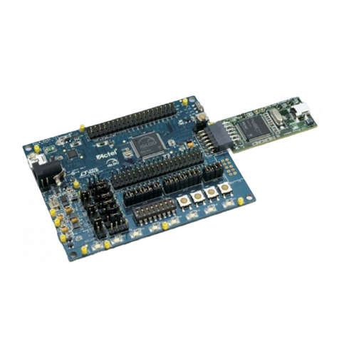
Avago HDJD-JD04 User manual

HDJD-JD04
Development Kit
Operating Hardware Manual
Introduction
Thank you for purchasing the HDJD-JD04 Development
Kit from Avago Technologies. The HDJD-JD04 Kit is a
simple development board, which demonstrates the
capabilities of the 20-pin ADJD-J823 color management
controller device with integrated RGB photosensors
as feedback device of an RGB LED-based backlighting
system.
The development kit can be used stand-alone with an
Autoload feature enabled, or connect direct to an IBM-PC
computer (using USB port).
Sample programs are provided to demonstrate the
unique features of the device.
The HDJD-JD04 Development Kit comes with the fol-
lowing:
•HDJD-JD04 Development Board (Figure 1-1)
•HDJD-JD04 FPC Board (Figure 1- 2)
•CD-ROM, which contains:
•HDJD-JD04 Development Kit Hardware User Guide
•ICMv2 Operating Software Manual
•Application Notes
•Datasheets
If you are missing any part of the kit, please contact your
nearest Avago Technologies sales oce listed in the back
of this publication for help.
AVAGO TECHNOLOGIES’ PRODUCTS AND SOFTWARE ARE NOT SPECIFICALLY DESIGNED, MANUFACTURED OR AUTHORIZED FOR SALE AS
PARTS, COMPONENTS OR ASSEMBLIES FOR THE PLANNING, CONSTRUCTION, MAINTENANCE OR DIRECT OPERATION OF A NUCLEAR FACILITY
OR FOR USE IN MEDICAL DEVICES OR APPLICATIONS. CUSTOMER IS SOLELY RESPONSIBLE, AND WAIVES ALL RIGHTS TO MAKE CLAIMS
AGAINST AVAGO TECHNOLOGIES OR ITS SUPPLIERS, FOR ALL LOSS, DAMAGE, EXPENSE OR LIABILITY IN CONNECTION WITH SUCH USE.
ESD WARNING: Standard CMOS handling precautions should be observed to avoid static discharge.
WARNING: This product is non RoHS compliant

2
HDJD-JD04 Development Board
The HDJD-JD04 development board has the following hardware features:
1. 20-pin QFN packaged ADJD-J823 device
2. Onboard +3.3V linear regulator with internal microprocessor reset circuit for direct input from +5V USB supply
or external +5V supply
3. 1K I2C Serial EEPROM
4. USB port and associated hardware for direct connection to a USB port interface
5. USB Data Transfer IC
6. Jumper to select either using USB +5V or external +5V
7. PCB mounting socket for external +5V supply
8. PWM output connector that connects to external LED driver card
9. HDJD-JD04 Flex Connector that connect the HDJD-JD04 exible circuit board
10. PWM output connector that connects to external LED driver card
11. External I/O connector that port various control pins of ADJD-J823 device externally
8910
11
5
6
4
7
Figure 1. HDJD-JD04 Development Board Hardware
1
2
3

3
HDJD-JD04 Development Kit Hardware User Guide
This guide describes the HDJD-JD04 Development Board, including hardware component layout and schematic.
Detailed information on ADJD-J823 can refer to the data sheet.
Chapter 1: Introduction - This chapter introduces the HDJD-JD04 Development Kit and provides a brief
description of the hardware.
Chapter 2: Hardware Description - This chapter describes in detail the hardware of the HDJD-JD04 Development
Board.
Reference Documents
Reference documents listed below are included in the CD-ROM.
•ADJD-J823 Technical Data Sheets Application Notes
•ADJD-J823 Application Note
•ICM Program User Guide
•HDJD-JD04 User Guide
Hardware Detail
The HDJD-JD04 Development Kit hardware is extremely simple and is intended to illustrate the ease of use of the Color
Management Controller with integrated RGB photosensors.
Power Supply
The development board has a linear regulator that will step-down the +5V input to provide +3.3V supply needed to
power up all the components onboard. The user can either choose USB +5V or external regulated 5V can be plugged
into J7.
The user can choose using the following jumper setting
J8 – External +5V
J9 – USB +5V
Note: The HDJD-JD04 Development Kit does not include a power supply.
USB Port
A USB port interface is provided for easy interfacing with an IBM-PC computer. The port is used to emulate I2C com-
munication using software to perform the communication translation job. The normal USB port cable can be used to
hook up the board with the computer.
Serial EEPROM
A M24C01 1K (128 x 8) I2C serial EEPROM, from Microchip, is included on the board to illustrate I2C bus concepts and
to store ADJD-J823 conguration and calibration data.
External Input-Output Connector
Most of the ADJD-J823 pins are mappable on the external input-output connector. These pins include:
•PWM output R/G/B (PWM R/G/B)
•I2C SDA (SDA)
•I2C SCL (SCL)
Sleep trigger (SLEEP)

4
Schematics
The following gures show schematics for the HDJD-JD04 Development board.
Figure 2a. HDJD-JD04 Development Board Schematic
1
2
3
4
5
CN1
CN-USB
3V3OUT
6
USBDM
8
USBDP
7
RSTOUT#
5
XTIN
27
XTOUT
28
RESET#
4
EECS
32
EESK
1
EEDATA
2
TEST
31
D0 25
D1 24
D2 23
D3 22
D4 21
D5 20
D6 19
D7 18
TXDEN 16
PWREN# 15
PWRCTL 14
TXLED# 12
RXLED# 11
SLEEP# 10
GND
9
GND
17
AGND
29 AVCC 30
VCC 3
VCC 26
VCC-IO 13
U3
FT232BM
C4
33nF
R5 27R
R6 27R
R7
470R
C5
0.1uF
5V
C6
10nF
R8
1k5
R9
2k2
C10
0.1uF
R10
10k
5V
5V
C11
10uF
C12
0.1uF
C13
0.1uF
3.3V
SCL
SDA
PWMR
PWMB
PWMG
GND
Spare1
Spare2
Spare3
Spare4
SLEEP
MR
Spare1
Spare2
Spare3
Spare4
5V
5V
3.3V
3.3V
GND
GND
1
2
3
4
5
6
J4
CON6
1
2
3
4
J5
CON4
JAZZ2 SystemBoard
L1
FBI 42R/100MHz
1
2
3
4
5
6
7
8
J3
CON8
SCL
SDADecouplingcapacitor for FT232BM
1
2
3
4
J6
CON4
MR
SLEEP
1
2
3
4
5
6
7
8
9
10
J2
CON10
5V
1
2
J7
CON2
1 2
J8
Ext 5V
1 2
J9
USB 5V
Y1
6MHz
C19
27pF
C18
27pF
J2, J5 is flex connector
J3, J4, J6 is header pin.
DO
4VSS 5
DI
3CLK
2CS
1VCC 8
N C 6
N C 7
U4
93LC46B

For product information and a complete list of distributors, please go to our web site: www.avagotech.com
Avago, AvagoTechnologies, and the A logo are trademarks of AvagoTechnologies, Limited in the United States and other countries.
Data subject to change. Copyright © 2007 AvagoTechnologies Limited. All rights reserved. Obsoletes AV02-0061EN
AV02-0500EN - July 4, 2007
N C 1
PWMB 2
PWMG 3
PWMR 4
DGND
5
DGND
6
DVDD
7
AGND
8
CLKIO 9
XRST
10
SCLS LV
11
SDASLV
12
SCLPROM 13
SDAPROM 14
SLEEP
15
AGND
16
AGND
17
AGND
18
AVDD
19
N C 20
U1
JAZZ2
3.3V
C1
0.1uF
C2
10nF SCL
1
VSS 2
SDA
3
VCC
4
WP 5
U2
24XX01B
R2
2k7
R1
2k7
R3
2k7
R4
2k7
3.3V C3
0.1uF
PWMR
PWMB
PWMG
SCL
SDA
JAZZ2 FPC
RESET
SLEEP
R11
2k7
C16
0.1uF
C17
10nF
3.3V
SCL
SDA
PWMR
PWMB
PWMG
GND
MR
SLEEP
3.3V
R12
2k7
3.3V
C14
1uF
C15
10uF
MR
5V
1
2
3
4
5
6
7
8
9
10
J1
CON10
5V
IN 1
GND 3
SHDN 4
RESET
5
MR 6
OUT
7
IN 2
OUT
8
U5
MAX6473TA33BD3-T
Figure 2b. HDJD-JD04 Development Board Schematic
AVAGO TECHNOLOGIES’ PRODUCTS AND SOFTWARE ARE NOT SPECIFICALLY DESIGNED, MANUFACTURED OR AUTHORIZED FOR SALE AS
PARTS, COMPONENTS OR ASSEMBLIES FOR THE PLANNING, CONSTRUCTION, MAINTENANCE OR DIRECT OPERATION OF A NUCLEAR FACILITY
OR FOR USE IN MEDICAL DEVICES OR APPLICATIONS. CUSTOMER IS SOLELY RESPONSIBLE, AND WAIVES ALL RIGHTS TO MAKE CLAIMS
AGAINST AVAGO TECHNOLOGIES OR ITS SUPPLIERS, FOR ALL LOSS, DAMAGE, EXPENSE OR LIABILITY IN CONNECTION WITH SUCH USE.
ESD WARNING: Standard CMOS handling precautions should be observed to avoid static discharge.
WARNING: This product is non RoHS compliant
Table of contents
Other Avago Microcontroller manuals