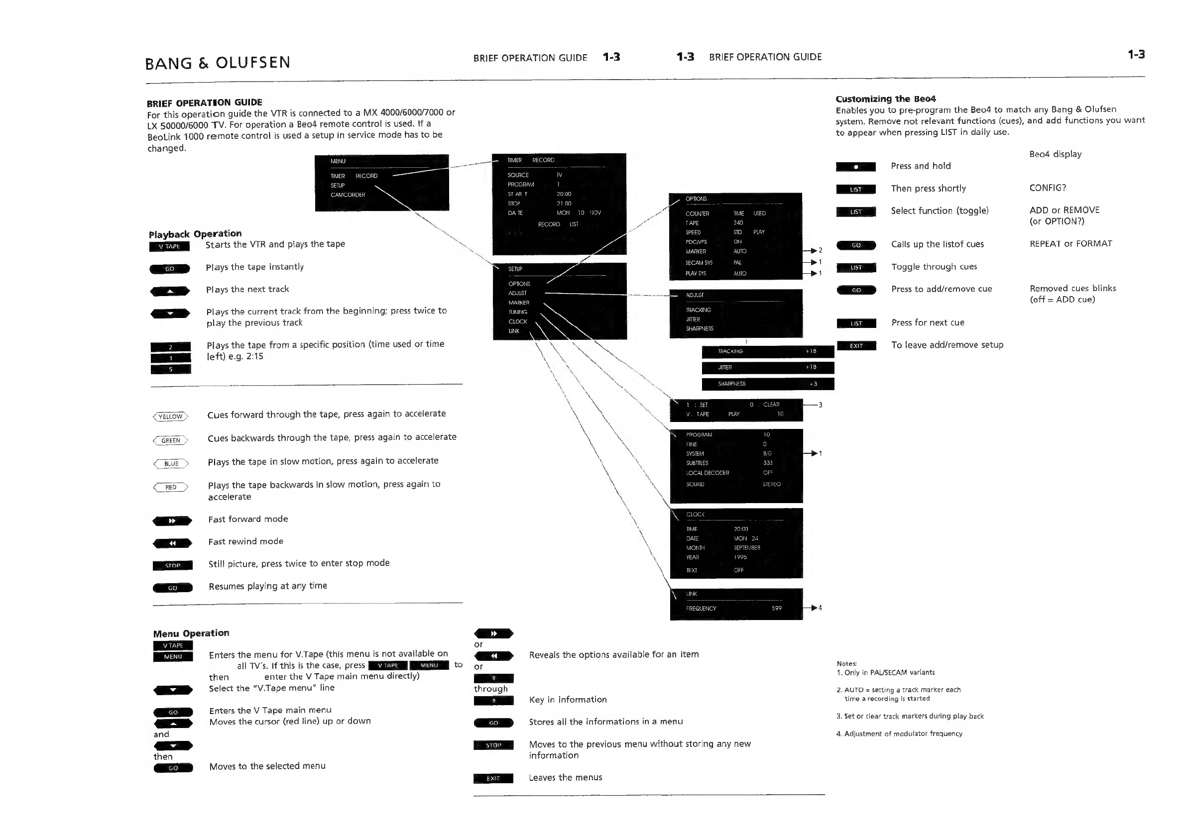
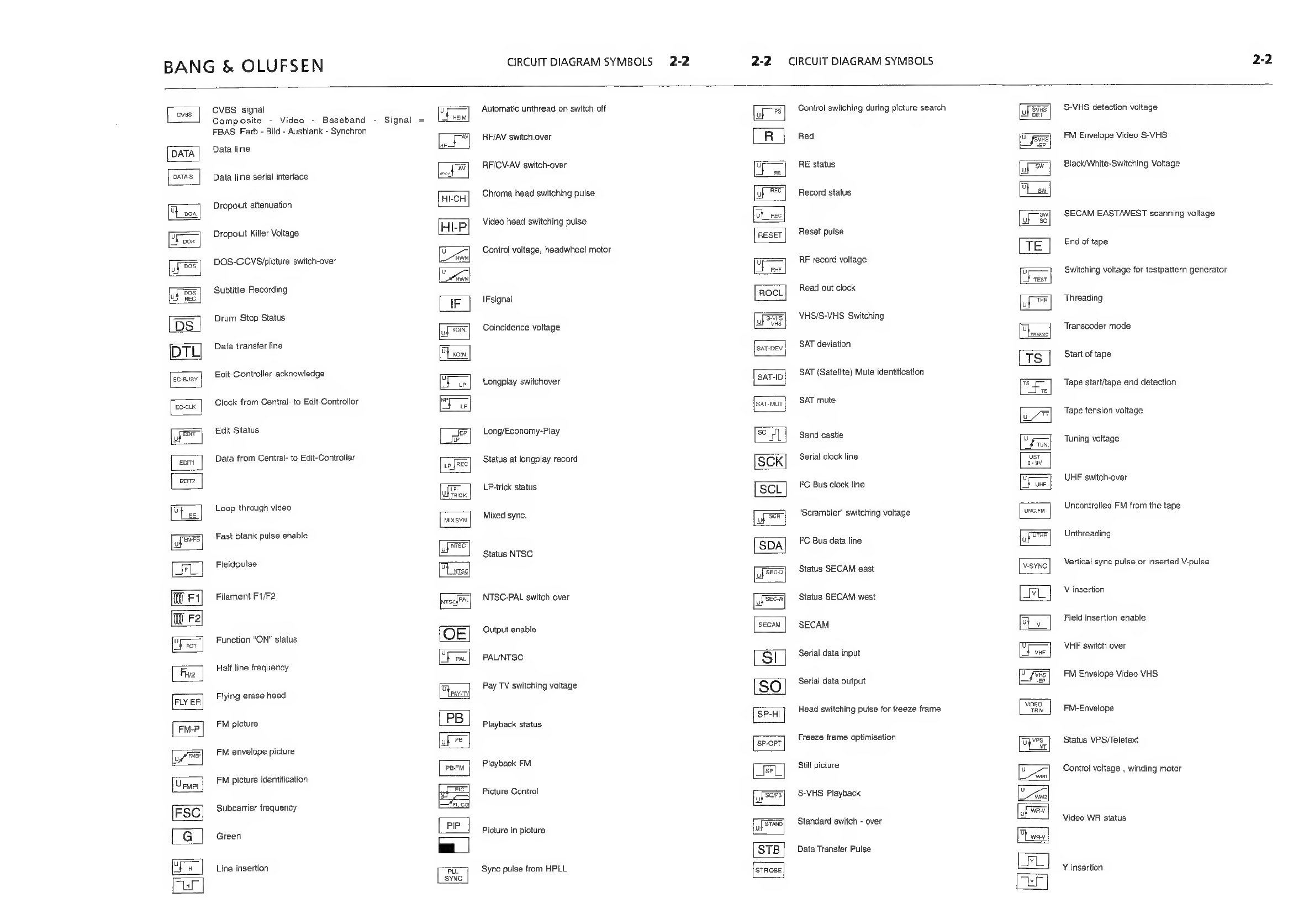
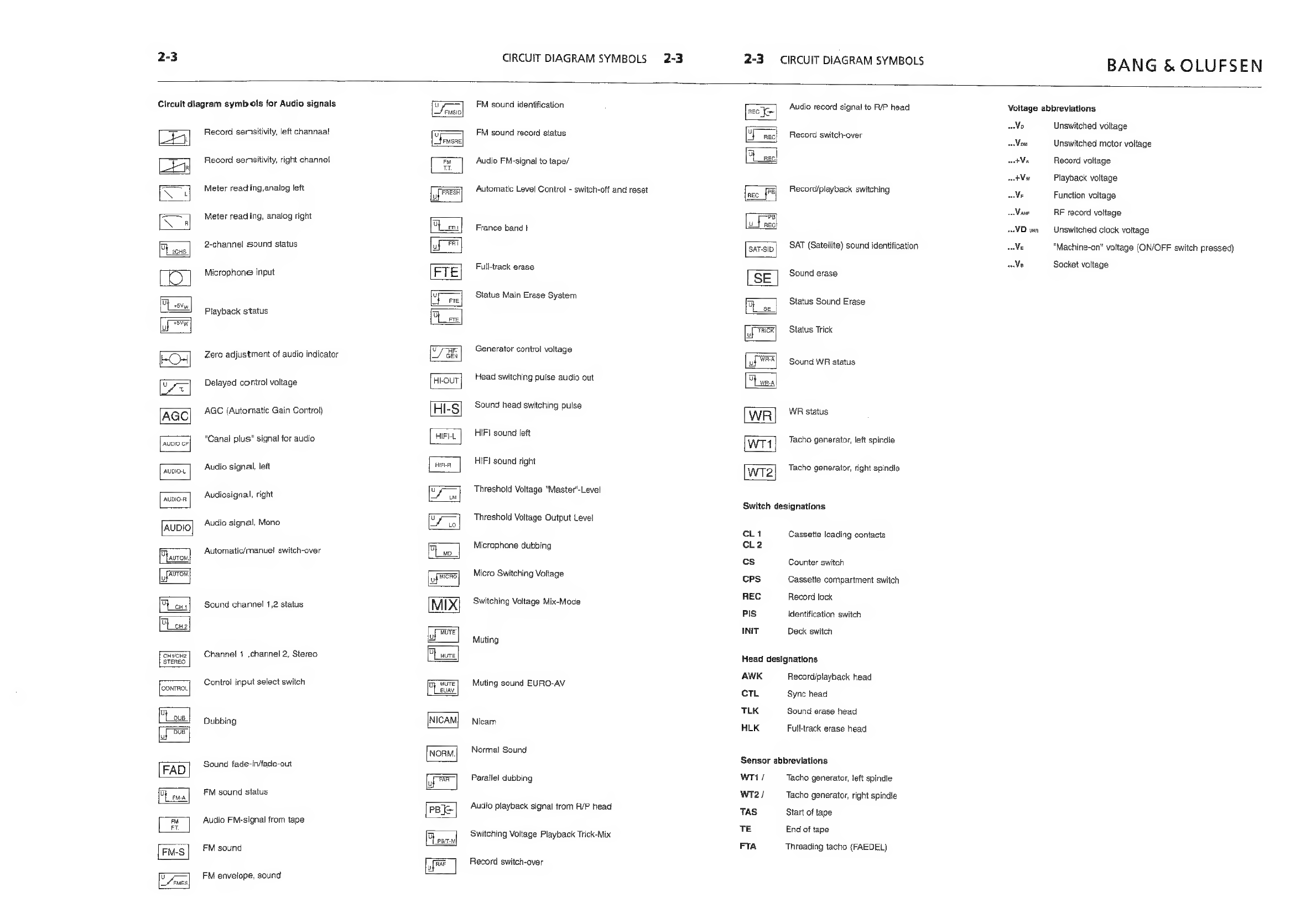
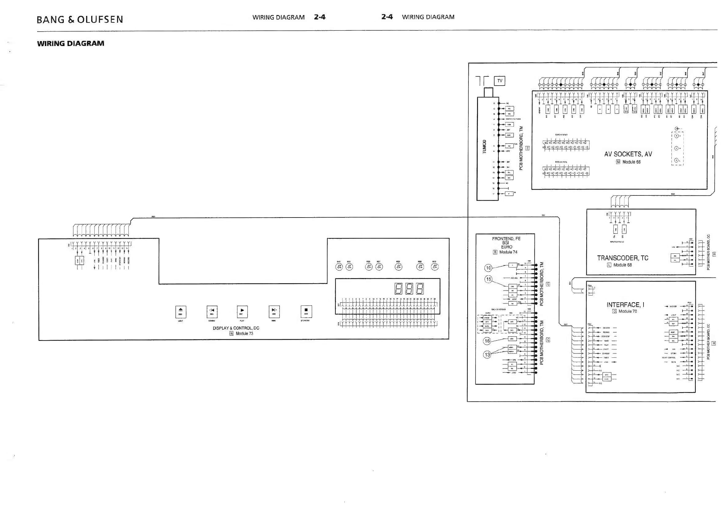
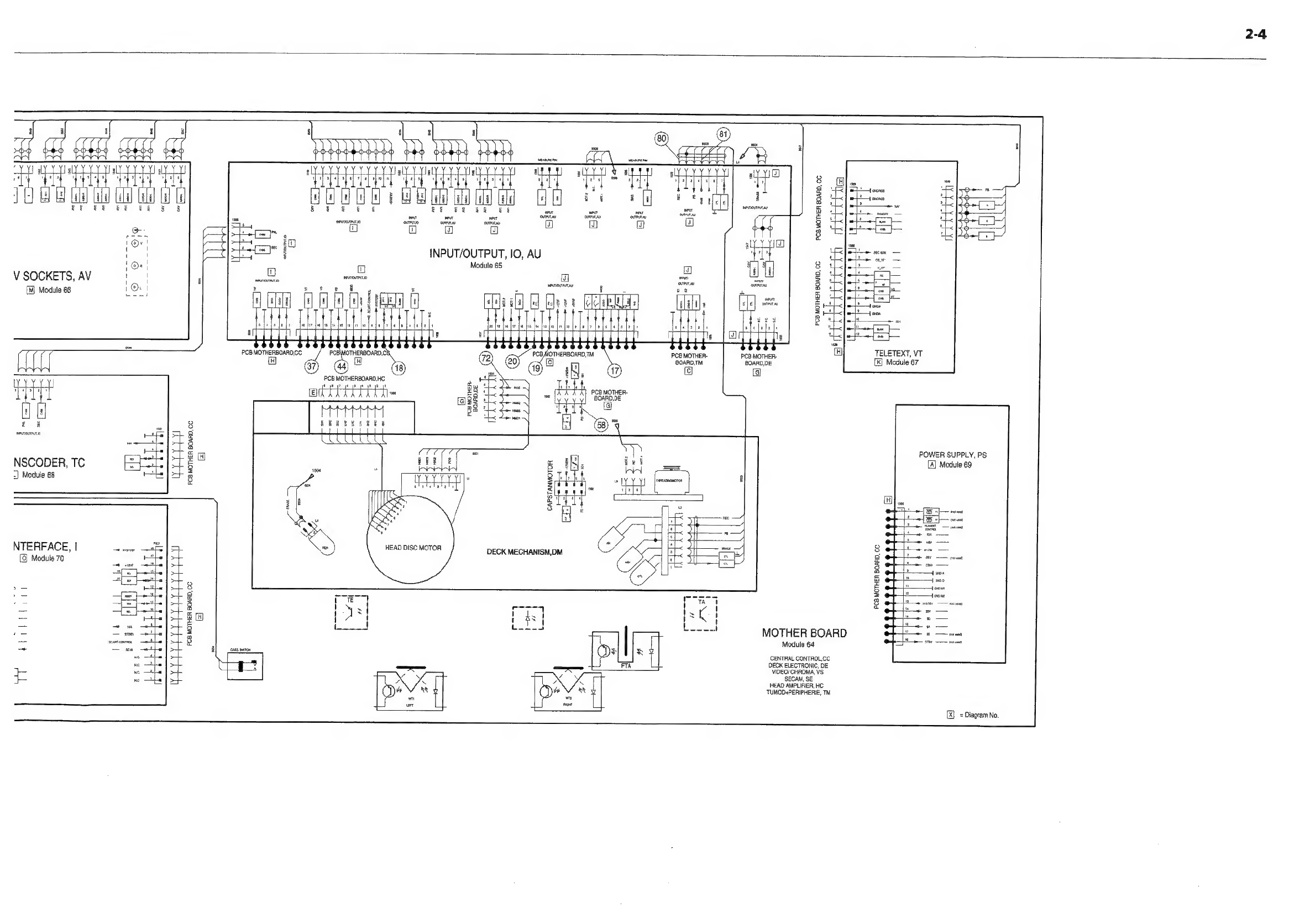
Bang-Olufsen BeoCord V8000 User manual

BeoCord
V8000
Type
4601,
4605,
4606,
4609
Service
Manual
English,
German,
French

CONTENTS
Survey
of
modules
..
=
Specification
guidelines
for
service
use
Brief
operation
guide
.
Diagrams
etc...
Explanation
of
diagram
Circuit
diagram
symbols
2-1
Wiring
diagram...
2-4
Block
diagrams
.
2-5
-
2-6
Diagrams.....
List
of
electrical
parts
3
List
of
mechanical
parts
4
Adjustments
and
repair
tips
..
5
English
German
French
Electrical
adjustments
5-1
5-34 5-68
Mechanical
adjustments
5-7
5-40
5-74
Repair
tips
5-10
5-43
5-77
Circuit
description
5-30
5-64
5-100
Dismantling
6
Insulation
test

BANG
&
OLUFSEN
SURVEY
OF
MODUL
1-1
1-1
SURVEY
OF
MODUL
1-1
64
Mother
Board
...diagr.
C,
D,
E,
F,
G,
H
page
2-15
-
2-20
65
Input
/
Output
.....
.
diagr.
1,
J
page
2-21
-
2-22
66
AV
sockets...
..diagr.
M
page
2-29
67
Teletext
.diagr.
K
page
2-25
68
Transcoder
...
.
diagr.
L
page
2-27
69
Power
Supply
.diagr.
A
page
2-8
70
Interface
..
71
Front
processor......
73
Display
and
Control
..
seen
Giagr.
N
page
2-30
74
Front
End
B/G
..
diagr.
B
page
2-9
74
Front
End
Multi
...
iagr.
B
page
2-12
95
Tape
Deck
complete

SPECIFICATION
GUIDELINES
1-2
1-2
SPECIFICATION
GUIDELINES
BANG
&
OLUFSEN
SPECIFICATION
GUIDELINES
FOR
SERVICE
USE
BeoCord
V8000
AUDIO
L
(WHITE)
/
R
(RED)
Audio
in
0.1V
RMS
to
2V
RMS
>
100kQ
Cassette
format
VHS
CTV
system
*
See
type
survey
Cabinet
finish
White,
Grey.
High-gloss
lacquer:
Pearly
black,
Pearly
green,
Pearly
red,
Pearly
blue,
Pearly
grey
Type
4606
Pearly
black
only
Remote
control
via
Beovision
Beo4
or
BeoLink
1000
remote
control
Tuner:
Tuner range
45-855MHz:
VHF,
S,
Hyper,
UHF
Number
of
TV
programmes
99
Play
channels
(Modulator)
471-855MHz
(default
599MHz):
UHF
Picture
function:
Max.
playing
time
video
SP,
4
hours,
LP,
8
hours,
€-240.
NTSC:
SP, LP,
EP
Max.
playing
time
audio
LP,
8
hours,
E-240
Playback
tapes
recorded
in
NTSC
3.58MHz
and
NTSC
4.43MHz
in
HiFi
stereo
sound.
|
S-VHS
(VHS
quality)
Fast
forward
and
rewind
Approx.
95
sec.
E-180
Slow
motion
foreward
and
reverse
1/2,
1/12
x
normal
speed
Still
picture
Noiseless
Search
(cue)
foreward
and
reverse
PAL/SECAM:
5
x
and
11
x
normal
speed
NTSC:
5
x
and
7
x
normal
speed
Counter
Track
marker,
time
left,
time
used
Recording
system
HQ
Rotating
tape
heads
2
SP
video,
2
LP
video,
2
Hi-Fi
sound
Signal-to
noise-ratio
luminance
(SP
mode)
>
4803
Signal-to
noise-ratio
chrominance
(SP
mode)
2
38dB
(AM),
2
31dB
(PM)
Sound
video
tape:
Sound,
compatible
Hi
Stereo
Hi-Fi/mono
fixed
head
Stereo
decoder
=
-
__*Nicam/A2
Frequency
range
20-20,000Hz
+/-3dB
Distortion
(Hi-Fi
mode)
<1%
VIDEO
IN
(YELLOW)
Video
in
1V,,
+/-
3dB
75Q
AV
&
V.TAPE
DECODER
Pin
1
Audio
R,,,
400mV
RMS
+1dB
<
1k
Pin
2
Audio
R,,
0.2V
RMS
to
2V
RMS
>
10k
Pin
3
Audio
L
out
400mV
RMS
+108
<
1k
Pin
4
Audio
ground
Pin
5
Blue
ground
Pin
6
Audio
L
in
0.2V
RMS
to
2V
RMS
>
10k
Pin?*
Blue
0.7V,,
750
Pin
8 Data
in/out
(AY)
Play
voltage:LogicO=Oto2V.
(4:3)
_
ae
Logic
1
=
9.5V
to
12V
(4:3)
=
Ry,
=
1k2
(43)
R,,
2
10k
~
(43)
4.5V
to
7VR,,,
<
1kQ
(16:9)
Pin8
Piay
voltage,
input
only
(TAPE
<2V
R,
>
10k
i
43)
DECODER)
=9.5V
R,>10k2
(43)
4.5V
to
7VR,,,
<
1kO
(16:9)
Ping
Green
ground
_
“Pin
10
Not
used
3%,
_Pint1*
Green
0.7V,,
758
.
Pin
12
Not
used
Pin13
Red
ground
Pin
14
Blanking
ground
Pin
15*
Red
0.7V,,
750
;
=a
Pin
16"
Blanking
=
~~
Logic
0
=
0
to
0.4V
=
Logic
1
= 1
to
3V
a
oe
-
“
Pin
17
Video
out
ground
Pin
18
Vdeo
in
ground
Pin
19
Composite
video
out
1V,,
+1/-2
dB
750
7
Pin
20
Composite
video
in
1V,,
+3/-3
dB
750
Signal-to-noise
ratio
>
63dB
(A-weighted)
Power
supply:
Mains
voltage
180-240
volts/SOHz
Power
consumption/minimum
Type
4601
and
4609
22
watts/2.1
watts
*
=
not
used
on
V.TAPE
DECODER
Subject
to
change
without
notice
Type
4605
and
4606
24
watts/2.1
watts
Dimensions:
WxHxD
38
x
9.7(incl.
feet)
x
28
cm
Weight
4.3kg
~
‘
—
Various:
Quickloading
Yes
Subtitles
from
Teletext
in
colours
‘
=
On
screen
display
Yes
Synchronous
Program
Recording
~VPS/PDC
Head
cleaning
___
Automatic
Timer
recording
8,
1
year
*TYPE
SURVEY
Modification
to
other
TV
transmission
systems
Type
System
Colour
NICAM
PAUSECAM
SYSTEM
B/G
é
4601
B/G
PAL
Eu
B/G
8005650
?
4605
B/G/LIL'/
PAUSECAM
F(GB)
—_—BIG/L/I
4606
BIG/DIK
PALISECAM
East
EU
_B/G/D/K
4609 /D/K
PAL
GB
I
1)
The
values
in
the
“VARIANT
SETUP”
must
be
changed
(see
section
5
Service
mode).
8005650
Transcoder
PCB

BANG
&
OLUFSEN
BRIEF
OPERATION
GUIDE
1-3
1-3
BRIEF
OPERATION
GUIDE
1-3
BRIEF
OPERATHON
GUIDE
Customizing
the
Beo4
For
this
operation
guide
the
VTR
is
connected
to
a
MX
4000/6000/7000
or
Enables
you
to
pre-program
the
Beo4
to
match
any
Bang
&
Olufsen
LX
50000/6000
TV.
For
operation
a
Beo4
remote
control
is
used.
If
a
system.
Remove
not
relevant
functions
(cues),
and
add
functions
you
want
BeoLink
1000
remote
control
is
used
a
setup
in
service
mode
has
to
be
to
appear
when
pressing
LIST
in
daily
use.
changed.
Beo4
display
MEO
and
hold
Then
press
shortly
CONFIG?
Select
function
(toggle)
ADD
or
REMOVE
(or
OPTION?)
Playback
Operation
Starts
the
VTR
and
plays
the
tape
Calls
up
the
listof
cues
REPEAT
or
FORMAT
GD
lays
the
tape
instantly
Toggle
through
cues
ED
"1a
the
next
track
Press
to
add/remove
cue
Removed
cues
blinks
rer:
é
(off
=
ADD
cue)
EMD
las
the
current
track
from
the
beginning;
press
twice
to
play
the
previous
track
Press
for
next
cue
Plays
the
tape
from
a
specific
position
(time
used
or
time
\
S
E
u
To
leave
add/remove
setup
MRECCieft)
e.g.
2:15
Keo
‘
_
wes
<YElow>
Cues
forward
through
the
tape,
press
again
to
accelerate
<CGREEN
>
Cues
backwards
through
the
tape,
press
again
to
accelerate
CBWE
>
Plays
the
tape
in
slow
motion,
press
again
to
accelerate
BLUES?
RED_
>
Plays
the
tape
backwards
in
slow
motion,
press
again
to
accelerate
xD
Fast
forward
mode
ED
fast
rewind
mode
Still
picture,
press
twice
to
enter
stop
mode
Resumes
playing
at
any
time
2
Menu
Operation
rF
>»
Y
or
Enters
the
menu
for
V.Tape
(this
menu
is
not
available
on
ED
Reveals
the
options
available
for
an
item
all
TV's.
If
this
is
the
case,
press
to
or
Notes:
then
enter
the
V
Tape
main
menu
directly)
20>}
1.
Only
in
PAUSECAM
variants
EMD
Select
the
“V.Tape
menu”
line
through
ok
,
2.
AUTO
=
setting
a
track
marker
each
Key
in
information
time
a
recording
is
started
Enters
the
V
Tape
main
menu
ED
Vovess
the
cursor
(red
line)
up
or
down
Stores
all
the
informations
in
a
menu
av
Set
or
clear,
srack
markers
curing
play
Back:
and
4,
Adjustment
of
modulator
frequency
<z=a@D>
Moves
to
the
previous
menu
without
storing
any
new
then
information
GO
Moves
to
the
selected
menu
Leaves
the
menus

2-1
EXPLANATION
OF
DIAGRAM
=
2-1
2-1
CIRCUIT
DIAGRAM
SYMBOLS
BANG
&
OLUFSEN
EXPLANATION
OF
DIAGRAM
Position
nos.for
the
components
Note
on
the
components
Connections
from
one
diagram
to
another
MEASURING
CONDITIONS
Symbol
of
safety
components
AN
Lithium
battery
1XXX
Crystals,
filters,
fuses,
connectors
etc.
2XXX
Capacitors
3XXX/_
Resistors
AXXX
5XXX_
Coils,
transformers
and
the
like
6XXX_
Diodes
7XXX_—
Transistors
and
IC’s
Components
marked
with
the
letter
“X”
means
that
the
component
is
planned
to
be
fitted.
Components
marked
with
the
letter
“Y"
means
that
the
component
is
used
only
in
certain
variants.
Example:
[DGR.F
(D1)
|
VS
2495!
DGR.F
(D1)|
=
The
other
end
of
the
wire
is
to
be
found
on
DIAGRAM
F
in
coordinate
no.
D1.
VS
2495
=
The
wire
in
coordinate
D1
is
going
to
capacitor
2495
in
the
Video/Chroma
circuits
on
DIAGRAM
F.
The
DC
voltages
and
oscillograms
are
measured
in
relation
to
ground.
The
DC
voltages
and
oscollograms
are
measured
in
RECORD
or
PLAY
mode,
with
a
colour
bar
signal
and
a
picture
carrier
at
503.25
MHz
(CH
25).
When
replacing
components
with
this
symbol,
components
with
identical
part
numbers
must
be
used.
The
new
component
must
be
mounted
in
the
same
way
as
the
one
replaced.
WARNING
Short-circuit
and
overcharging
of
some
types
of
lithium
batteries
may
result
in
a
violent
explosion.
When
replacing
the
lithium
battery
in
this
set,
note
the
following:
Use
only
batteries
at
the
same
make
and
type
as
mentioned
in
this
service
manual
(see
page
3-4).
Place
the
battery
exactly
like
the
old
one.
ADVARSEL
LITHIUMBATTERI
-
EKSPLOSIONSFARE
UDSKIFTNING
MA
KUN
FORETAGES
AF EN
SAGKYNDIG
0G
SOM
SESKREVET
|
SERVICE
MANUAL,
WARNING
|
LITHIUM
BATTERY
-
RISK
OF
EXPLOSION
‘TO
BE
REPLACED
BY
QUALIFIED
SERVICEMAN
ONLY
‘AND
AS
DESCRIBED
IN
THE
MANUAL
Circuit
diagram
symbols
Circuit
diagram
symbols
for
video
signals,
chroma
signals
and
status
commands.
Various
signals
on
one
lead:
Record
BD.
I/II
switch-over
eam
Playback
D
TAME
1.1
MHz
Signal
(SECAM)
ves]
Aspect
ratio
16:9
2Fgc]
Double
subcarrier
frequency
we]
Aspect
ratio
4:3
WL]
Oplocoupler
pulses
[]]
Frame
carers]
627 KHz
Signal
(PAL)
Chassis
Reference
potential
Seperate
chassis
connection
Switching
voltage
for
record
ARG]
Voltage
dependent
on
the
selected
frequency
Control
voltage
for
MENU
signal
bar
7100008
at]
AM/FM
switch
over
aa
==]
Automatic
Tuning
Search
Level
Ae
Status
f.
auto
SECAM
switchover
Zura
|
Autom.
SECAM-EAST
identification
AV
switching
voltage
Status
for
the
switching
voltage
onAV-I
Evaluation
of
an
external
switching
voltage
Switching
voltage
on
AV-|
(dependent
on
the
evaluation
of
U-AV.II)
Blue
BD.
III
switch-over
Burst
Key
pulse.
Signal
Blanking
CVS
BLANK
qe
Sutching
Sa
with
DOS
or
OSD
superimposed
on
a
ud
BE
TP
ae].
Field
Memory
Status
Ear]
Sense
of
Rotation
CAM
|
Camera
cCvs
roan,
Selo
-
Video
-
Signal
CH
Chroma
signal
vu
oH
Chroma
envelope
(Video)
CLK
Clock
line
CLOCK
Gocws]
Clock
line
serial
interface
TZ]
Contol
vata,
capstan
motor
wPEE]
Black
White-Colour
Switching
Voltage
[fear]
Y/C
component
input
signal
Gonrw]
Controlled
FM
Commas}
Remote
Control
Data
via
the
CONTROL-S-socket
oe
|
[uf]
Canal
Plus
LCTL]
sync
pulse
[SYN]
[Fz]
Threshold
Voltage
Crispening
CV
status
CV/RF
switch-over
Video
signal

BANG
&
OLUFSEN
CIRCUIT
DIAGRAM
SYMBOLS
=
2-2
2-2
CIRCUIT
DIAGRAM
SYMBOLS
2-2
CVBS
signal
FBAS
Farb
-
Bild
-
Ausblank
-
Synchron
DATA
Data
line
bea
oe
Data
line
serial
interface
Dropout
attenuation
Dropout
Killer
Voltage
8
DOS-CCVS/picture
switch-over
:
Subtitle
Recording
=
EE
Drum
Stop
Status
DTL
Data
transfer
line
Edit-Controller
acknowledge
EC-BUSY
EC-CLK
Clock
from
Central-
to
Edit-Controller
Edit
Status
eo
Data
from
Central-
to
Edit-Controller
eorr2
ry
Loop
through
video
«
TPE]
_
Fast
blank
pulse
enable
FAL]
Fieldpulse
)
F
1)
Filament
F1/F2
Function
"ON"
status
FOT
Riga
|
Halt
line
frequency
Flying
erase
head
FM
picture
[7as]
FM
envelope
picture
FM
picture
identification
FSG]
Subcarrier
frequency
G
Green
oF
a
Line
insertion
Composite
-
Video
-
Baseband
-
Signal
tp
[REC
T
ub
Tick
Mx
SYN
ur]
FE
PLL
SYNC
Automatic
unthread
on
switch
off
RF/AV
switch.over
RF/CV-AV
switch-over
Chroma
head
switching
pulse
Video
head
switching
pulse
Control
voltage,
headwheel
motor
IFsignal
Coincidence
voltage
Longplay
switchover
Long/Economy-Play
Status
at
longplay
record
LP-trick
status.
Mixed
sync.
Status
NTSC.
NTSC-PAL
switch
over
Output
enable
PAL/NTSC
Pay
TV
switching
voltage
Playback
status
Playback
FM
Picture
Control
Picture
in
picture
Sync
pulse
from
HPLL
u
SAT-ID
[sat-MuT
se
SCK
SCL
uf
SF
SDA
[ap
Se
Rea
SECAM
Sl
SO
SP-HI
SP-OPT
Control
switching
during
picture
search
Red
RE
status
Record
status
Reset
pulse
RF
record
voltage
Read
out
clock
VHS/S-VHS
Switching
SAT
deviation
SAT
(Satellite)
Mute
identification
SAT
mute
Sand
castle
Serial
clock
line
°C
Bus
clock
line:
"Scrambler"
switching
voltage
FC
Bus
data
line
Status
SECAM
east
Status
SECAM
west
SECAM
Serial
data
input
Serial
data
output
Head
switching
pulse
for
freeze
frame
Freeze
frame
optimisation
Still
picture
S-VHS
Playback
Standard
switch
-
over
Data
Transfer
Pulse
ThA
Mensse
i
TS
is
TE
TUN,
o-wv
HE
uNe.FM
fioaal
V-SYNC
TEI
I
ve
“EP
VinEO
TRIV
mf
Wav
4
gy
wee
e/a
S-VHS
detection
voltage
FM
Envelope
Video
S-VHS.
Black/White-Switching
Voltage
SECAM
EAST/WEST
scanning
voltage
End
of
tape
Switching
voltage
for
testpattern
generator
Threading
Transcoder
mode
Start
of
tape
Tape
start/tape
end
detection
Tape
tension
voltage
Tuning
voltage
UHF
switch-over
Uncontrolled
FM
from
the
tape
Unthreading
Vertical
sync
pulse
or
inserted
V-pulse
V
insertion
Field
insertion
enable
VHF
switch
over
FM
Envelope
Video
VHS
FM-Envelope
Status
VPS/Teletext
Control
voltage
,
winding
motor
Video
WR
status
Y
insertion

2-3
CIRCUIT
DIAGRAM
SYMBOLS
=
2-3
2-3
CIRCUIT
DIAGRAM
SYMBOLS
BANG
&
OLUFSEN
Circuit
diagram
symbols
for
Audio
signals
Record
sensitivity,
left
channaal
Record
sensitivity,
right
channel
I
hy
iy
Meter
reading,analog
left
Meter
reading,
analog
right
And
2-channel
sound
status
Microphone
input
=)
playback
status
lw
Zero
adjustment
of
audio
indicator
8
GBE
Delayed
control
voltage
5
AGC
(Automatic
Gain
Control)
AGC
oe]
"Canal
plus"
signal
for
audio
wor]
Audio
signal,
left
moon]
Audiosignal,
right
AUDIO)
Audio
signal,
Mono
FF
‘Automatic/manuel
switch-over
"_cui|
Sound
channel
1,2
status
‘CHICHE
Channel
1
,channel
2,
Stereo
Control
input
select
switch
a
Dubbing
Sound
fade-in/fade-out
FAD
cua]
FM
sound
status
fi]
Audio
FM-signal
from
tape
rt
Fucs]
FM
sound
T
FM
envelope,
sound
2
Anes
HFA,
FM
sound
identification
FM
sound
record
status
Audio
FM-signal
to
tape/
Automatic
Level
Control
-
switch-off
and
reset
France
band
|
Full-track
erase
Status
Main
Erase
System
Generator
contro!
voltage
Head
switching
pulse
audio
out
Sound
head
switching
pulse
HIF
sound
left
HIFI
sound
right
Threshold
Voltage
"Master’-Level
Threshold
Voltage
Output
Level
Microphone
dubbing
Micro
Switching
Voltage
Switching
Voltage
Mix-Mode
Muting
Muting
sound
EURO-AV.
Nicam
Normal
Sound
Parallel
dubbing
Audio
playback
signal
from
R/P
head
Switching
Voltage
Playback
Trick-Mix
Record
switch-over
meee]
Audio
record
signal
to
PUP
head
rec]
Record
switch-over
neo}
Fa]
Recordiplayback
switching
PB
wt
rec]
‘sat-sip|
SAT
(Satellite)
sound
identification
Sound
erase
SE)"
z
Status
Sound
Erase
TAR
‘Status
Trick
ul
“F4)
Sound
WR
status
WR
WR
status
WT]
ache
generator,
lett
spindle
We]
Tacho
generator,
right
spindle
Switch
designations
cli
Cassette
loading
contacts
cL2
cs
Counter
switch
cps
Cassette
compartment
switch
REC
Record
lock
PIS
Identification
switch
INIT
Deck
switch
Head
designations
AWK
Record/playback
head
CTL
Syne
head
TLK
Sound
erase
head
HLK
Full-track
erase
head
Sensor
abbreviations
WT1/
acho
generator,
left
spindle
WT2/
——Tacho
generator,
right
spindle
TAS
Start
of
tape
TE
End
of
tape
FTA
Threading
tacho
(FAEDEL)
Voltage
abbreviations
Vo
Unswitched
voltage
Unswitched
motor
voltage
Record
voltage
Playback
voltage
Function
voltage
RF
record
voltage
Unswitched
clock
voltage
“Machine-on"
voltage
(ON/OFF
switch
pressed)
Socket
voltage

2-4
WIRING
DIAGRAM
WIRING
DIAGRAM
2-4
BANG
&
OLUFSEN
WIRING
DIAGRAM
AV
SOCKETS,
AV
[i]
Module
66
=
90
“akvOR
YBHLON
God
Lesver
TC
Module
68
INTERFACE,
|
{©
Module
70
TRANSCODER
ra)
=
90
'aUvO8
HSHLOM
20d
3
Er
Module
74
w
ira
=
2
ini
B
6
&
&
]
WL
‘GHOBYSHLOW
8od
a
WL
‘GHOBHSHLOW
80d
TTT
TTT
Erevessesrs
DISPLAY
&
CONTROL,
DC
(W)
Module
73

2-4
®
i
1
1
ic)
V
SOCKETS,
AV
[H
Module
66
'
ie
yy
++
NSCODER,
TC
re
=]
Module
68
mo
ty
PCB
MOTHER
BOARD,
CC
&
NTERFACE,
|
ee
[©
Module
70
eridddaa
/
“H+
PCBMOTHER
BOARD,
cc
Ea]
Hise
INPUT/OUTPUT,
10,
AU
Module
65
IES}
1F
Dot
PCB
MOTHER
BOARD,
CC.
PCB
MOTHER
BOARD,
CC
ali
DECK
MECHANISM,DM
el
&
aa
MOTHER
BOARD
Module
64
CENTRAL
CONTROL.CC
DECK
ELECTRONIC,
DE
VIDEO!
CHROMA,
VS.
SECAM,
SE
HEAD
AMPLIFIER,
HC
TUMOD+PERIPHERIE,
TM
TELETEXT,
VT
BOARD.DE
(K)
Module
67
g
PCB
MOTHER
BOARD,
CC.
ft
ik
POWER
SUPPLY,
PS
Module
69
(B=
Diagram
No

2-5
BLOCK
DIAGRAM
ANALOG
Module
65
s
hi
.
7a
ee
ee
eee
an
“
.
peo
a
7 7
3
a
|
AV
BOARD
Module
66
Be en
Rae
eet
1/0
BOARD
Mostle
OB
6s
=——
Tide
oases
FM
BART
7
.
-
3
Al
wore
as
ME
‘hie
Ce
i
4
a
LOsIe
”
a
M
(oeco0e8)
AUDIO
(AU)
i
a
po
7
ys
0
/
| i
\
Td
2
2
mo
woes
&
rete
2
Ler
out
wl
I
so
sh
[ot
a
aass
4
en
ma
t
nean
even
=
ut
£2
RIGHT
OUT
20)
1
¥
:
aan
Co
'
J
ts:
AUDIO
Lit
F,
Aare
al
Fal
ee
|
sot
a
ae
a4
Spe
=
|
—
|
i
[es
|
‘bio
MoD
ot
Pq
+
+
Te
f
Pa)
oneen
i
1
;
i
t
F
ous
wre
|
7
3
ls
:
3
ma
A
‘
ama
X
t
g g
+
st
ses
{|
sys
a
0
_t_
3
dg
ae
he
aunet
viet]
ass
|
~
=
as
sa
he
7
]
8]
|
on
|
flo
SL,
exo
ou
anges
|
arse
|
ai
2
ul
Lisa
moe)
t
in
su
ous)
36S
a)
|
YY
Ser
er
our
wisae
|
5/1548
i
ay
fas
J
iis47
avo
e
8.
fer
;
22:
t
FETA
AES
ee
we
1
(x
1
oat
:
a
al
|
Sener,
sree
[ys
SHS
bebe
ot
|
=
:,
*
3
2
2
Lprsor
at
Pasa
|
eer
CuARWEL,
Bato
[Bioo
_-e{uumen
}
Fan
19
hcg
'
7
<1 kh
£)
LEFT
5/1546
acc
|
wu
1
a
©]
ser
ue
7/7099"
ED
GAT
Oe
Pa
RIES
I
'
6
|
|
fu
ro
wee
(rue)
\
sarresr
iy
a
3 2
a
a a
a
=
=
“=
ae
280
rt
|
ql
alis
!
i
io
av
pase,
upo-e
SCN
ran
ne
oO
)ARD
i
te
| 7
|
i
=
7
7
|
3
=|
g
[SenRo.
T
Ne
FER
'
ee
‘ee
i
Pm es
s
.
—
- -
H
3]
|
|
sleito
8
hate
En
‘SECAM
(SE)
aE
]s
Lees
rv
es
eae
verso
a
SL]
|
st
1
Bel8)
3
vere
][feme
—
(—e
es
ee
'
[
B
re
:
4
aye
3
aie
4
beens
7B
6
Sd
tei
dea
ped
eS
MOTHER
BOARD
MODULE
64
_ - .
ea
inva]
ae
rah
Gy
ie
- -
-
ofa
ie
Sai
eee
CRE
REED
‘
2
'
=
Ey!
Suuricd
H
werw
a.
MOBO
(TM)
TELETEXT
(VT)
|
R6BOFF
ips
=
:
tH
care
-
SL
|
Module
67
Y
LT
Data
3/4
i
DATA
S
!
eH}
r!
4
bem
Prce
FEC
gy
1
i
(
is
omer
" e
0,
=
aaa]
|
=
ssl
io}
2lils
'
13/1625
aprerst
43/1628
FE
BOARD
Sees
|
|
gl
'
=]
=
770
i!
CHROMA
PROCESSING
4
i
Por
if
FRONT
ENDIF
SSP
|)
&
ast
H
Dar
ASTER
8
Sarr
REOSTER
6
‘lt
¥
SECAM
L
!
|
=
5
ai
i
Pi
ct
TE
|
fee
!
sot]
[soa
:
1
iene
v
v
rf4
peg
ryyo}
Ince
!
je.
ara
git
pzisz9"
H
i
Wee
Ff
1
am
ic
¥
200)
38
[30
\
Hug
A
1
fe
cock
rahe
2.4
1
2
1
g $
=
scam
'
wom
2
1
Eo
ane
—
38
vaca
cones
|
!
ib
1
‘
és
1
cio
Sara
|e
sie
|
(34)
202
Ra
|
ines
|
nse
Ste-e
L
| |
Fj
etl
io
l
ee
a
vio
IAL
PROCESSING
(vs)
[F]
2
7080
Aubo
eset
+
H
1]
eer
SeNPUTOUTPUT,,
,.,.]
[TRANCOGERITCT
Modueds
Beer
EO
SIaM
a]
.
velba
Ai
UE)
|
(7th
eee
an
]
:
Fee
|
oe
x
Hh"
x
nn
16
ue
etal
oe
1
added
ad
|
Ire
sa
211838
iv
SH
tee
|.
sremcoy
[14
AOIO-R
J
|)
[rao
peoface
HST
|
s1s20}
3/1538
Fest
yecras
A
2
7
TR
|
au
Prove]
pang
sl
arto.
2)
Benson
|
€
bs]
+
[8
f
PS
Toco
PUBS
TTT
AD
pete
oar
Ce)
KI
ocdSte|
83)
/re
*
bon
se=
Pa
ain
|
fe
iL
ss
(16
'
-
il
ees
ao
ajo:
|
|
WAY!
TL
raze
_|
[woso
icon
‘Ties
os.
BS
sates
Z
mie
ane
Fei:
co
5,
|]
[Ee
:
-
[nse
—_
1
eae
age
rye
&
Te
:
tl
r)
Eas]
=]
ise
:
©
our
ofr
|
Paes
=
Fay
SRS
we
|
‘ats
Soo
—*yheteer
ey
LVM)
sl
ice"|
fy
Be]
)
ee
Fee]
fa
b
uy
%
|
os
|
Tah
-_—-
———
ee
ws
|
so6w
——
(@)
TR
2
vs
vw
ue]
sn
——_—
!
ov
neg
=
a
ora
|
H
ee
er:
x
|
os
|}
ri
|
we
Peed
all
a
285.109
-
feast
Ls
en
[4
“a
1
——
<1
|
oe
|
HT
ie
1
:
NER,
-
wt
‘
tS:
h«
L_
Le
1H
'
ch
gre
Meputor
[sf
_——-
acum)
oo!
2369
8/2
a
ree
em
ares
Spevel
[E]
Lash,
of
cows
[2s
fon
PPR
me
ES7EM"a
ioc
ra
‘
-
ide
RULER
Aveo.
||
cuawe
rg
ial
|
vat
ul
ae
0
_[oowrrou
a7]
Ta]
FRTER
le.
"etwnn|
it
=W
TR
wane
Ha
.
a
Lips
La
is
sro
~
cool
RE
“
eS
xe
os
ct
nes
==
ST
Coca
eee
—_
aaa
Ete
ya
a
as
z
Sh:
jeer
i
—
1
yaya
T
Tree
bocel
ae
[D
Lor
a)
i
i
TL
00
<a—
1
le
Be
Te
t
|
se
a
ERIN,
F
4
*
i
; :
1
waza
ll
7
Smt]
=
[wool
AY
iahy
a
y
is
2
:
H
ae
He
‘smoosesey
||
8
BY
|
sn
ae
465
{simon
Vib
i
fl
'
4
a
cowrai]
[PLL
a
asses
roe
Saanee
"75°
‘
F
Lye
wom
|
vo
E
s
the
:
SE
MN
1
|
Uf
FEPCROTISCE
ose
scxo8]
Seat
:
'
Eyot
ater
ened
spied
ritp
oo
a
2!
¢€
ob
yee
700
wepeu bores
!
SECAMise)
|
hae
MOTHER
BOARD
="
soa}
|
sot
i
+
+
T
SOF
1
|
|
TUNER
MODULATOR
(TM)
EY
nm
7
sci-F
[hea
Ev
- = =
= +
2
z
=
5 =
=
Fi
ae
=
=
x;
=
a
a S
7 %
S
Z
7m
=
a
a
"=
RECORD
VIDEO
=>
RECORD
AUDIO.
=e
a
en
a

BLOCK
DIAGRAM)
2-5
2-5
BLOCK
DIAGRAM
BANG
&
OLUFSEN
uO
VELL
3
no
ee
ay
oo
LEVEL
R
ajresr
oat
“sn
10
Ln
als
%
we
ses
|
une
Nea
PLAYBACK
fuse
‘AUDIO_LINEAR
PART
|
a
5/1893
|
&
700
Tabi
|
a
ec
wee
b
2s
2
Us
isos
1
SOBA
MF
i
Rec/Pe
pe
:
fc
es
rec
|
Ise
yysos
|
1
2
use
LS}
vise
|
_HeAo
a
wt
tewes)
3/5657
pean
sca
1
—H
IR
i
H
————e
oe
pa
ieee
(eee
HEAD
AMPLIFIER
(HC)
f
A
To
WE
(ue)
re
ae
ee
lea
on
H
samen
we
128%
Pane
|
21
T
spears
es
(pa)
1/937
er
ol
i
‘
ee
net
—_]
<
7
|
:
S85
Fu
FT
(FP)
637
use
=
|;
Ze
mi
Se
er
ee
oat
r=
AS
seco>|
(20
ars
Tero
6
Bro
3
ey]
penne
va
2
eae
|
wr
2a
mi
7"
ae
poi
-Rec~
—
=
20
8_foxa
of
21
o
see
5
|
16S
|
eroce
y
758
rors
it
te
|
—_—
vy
|
:
eo
Ema
Pores
.
F
oe
auto
sec
rary
|
a
+
i
0
38
‘9
al
fi
iro
see
a
TOE
ere
T
ri
38
—_
i
TAG.
jaec
|
Tree
\
=
wl
oa
ete
:
@
ar
conrmasy
|
PB
40
L
nem
pur
a
iE
|
x]
vet
Lowe
noe
4
2
4
fone
Me]
|2s
t
ewetomraue)
|
A
LA
t
1
us
-
.
iS
ET
@)
ist
Fone
[Ay]
seu
Love
ar
a
ae
ws
|
TRV
3
wa
eal
f
x
Pee
7
ti
-
oe:
[F
forec
zt
:
(ooeoue
oye
ony
K
loec
a
ap
Be
_
23]
qe!
+
onaore
|
UT
H
conbaoR
Bovgonna
Ter
=
SOF
[fc
us
set

BANG
&
OLUFSEN
BLOCK
DIAGRAM
2-6
2-6
BLOCK
DIAGRAM
BLOCK
DIAGRAM
DIGITAL
CAPSTAN
MOTOR
UNIT
\0
BOARD
MOTHER
BOARD
DECK
ELECTRONICS
(DE)
Module
64
_
. “
"
S f a =
-
—.
a
= = - - 5 -
=a
DECK
CONTROLLER
oe
OF
a
CAPSTAN
MO
reyes
1s
ss
7oas
rweaiesea
|
a
393
Pa
Pu
cone
1743687
__swor
2
MOTOR
DIRECTION,
40]
(50)
(68)
L
Nt
|
|
west
—“dast
(68
(48)
i
!
ad
|
i
[Ao
|__seeb
6/1503
7080-4
|
me
10
cates
|
S
i
Os
on
__a/sg0gy
tone
;
CTL
PROCESSING
|
z
7086-8
Sik
1310
—
bo
vsemse
2
36
8c?
2
|
"iI
a
=
19
ROT
|
|
|
|
|
:
he
ense
qo
Letts
«roe
{~F
|
|
= ;
|
PON
ERATOR
3
|
seker
ec
re
sw
I
Te
8
sa
cor/e,
capstan
RECTION
/
Zi
for_mec
38
th
3000
aa
2
eT
be
=
“=f
]
oman?
3
ms)
38
@
2
ti
Tey
rues),
50
|
es
le
sexes
SSP)
wa
1095
Bes
|
|
16
HMos
POWER
SUPPLY
(PS)
Module
69
>
>
wre
iy
on
a
sol
1
a
i
7
—_
cao
i
E
20
ono
eae
j
a
|
707
:
Hl
HARDWARE
=
a
;
rex]
|
|
PROCESSOR
[25
—
36
ea
eee
ace
‘
a
s
as
-
:
ake.
7
—e
%
a
=
2
—
wee
=
att
—
ee
pee
meee
many
ofl
S
——
ae
202
INTERFACE
PCB
(CU)
Module
70
[0
FRONT
PCB
(DC)
Module
73
3
Lt
Ee
=e
me
LATCH
Raw
Hi
the
' :
o
N
'
evox
2
p—
ne
o1seAy
i
STROBE
3
ao
2
maa
'}
1
a
3
i!
‘
ri}:
=
.
cereus
ri
soy
Reser
(==
Fh
A
en
OG
‘
|
oo
stor
iss
: A
Bele
i
183
a
mere
"lg
1]
SS
aa
suey
' |
silal_
ois
sexe,
sent
uNK
Gerieerh
rl
SCART
CONTROL
e/i83}
uP
FEP
!
q
Se
8
ay
7
Wisy
|—
:
d
¢
|
|
:
15/5
[a
>
=
i
Son
eee
we
:
i
I
<1
sa
o/s
|
eibee
}—o00r
+
:
a
Z|
~=
i
febes
a
08
A:
DC,
SOO/
CONNECTC
A:
DG,1V/E
1
7100
PIN
A:
DC,
SOOF
CONNECTC
A:
DC,
500/
CONNECTC
A:
DG,
1V/E
CONNECTC

2-6
A:
DC,
SOOMV/DIV,
10US/DIV
CONNECTOR
1624
PIN
10
TREC
:
B
Ll
ere
eee
i
eg
ov.
A:
DG,
1
V/DIV,
SOOUS/DIV
IC
100
PIN
11/12
REC
15
Loli
eh
dy
ag
A:
DC,
SOOMV/DIY,
20US/DIV
CONNECTOR
1624
PIN
5
A
TA
REQ\
16
Fy
A
i
tA
A
pa
ae
ee
ee
een
ee
au
A:
DC,
SOOMV/DIV,
500US/DIV
CONNECTOR
1625
PIN
9
TREC
17
ov
A:
DC,
1
V/DIV,
500US/DIV
CONNECTOR
1637
PIN
5
L
Baiablec
A
L
ov
A:
DC,
SOOMV/DIV,
20US/DIV
CONNECTOR
1638
PIN
7
A:
DC,
1OOMV/DIV,
100NS/DIV
CONNECTOR
1637
PIN
12
A:
DG,
10OMV/DIV,
1MS/DIV
CONNECTOR
1637
PIN
12
“pp
20
i
i
z £
4
ov
A:
DC,
SOOMV/DIV,
100NS/DIV.
CONNECTOR
1637
PIN
14
A:
AC,
2OOMV/DIV,
1MS/DIV
CONNECTOR
1637
PIN
14
A:
DC,
SOOMV/DIV,
1US/DIV
IC
7600
PIN
19
TREC
A:
DC,
SOOMV/DIV,
10US/DIV
CONNECTOR
1638
PIN
12
A:
AG,
2OOMV/DIV,
20US/DIV
IC
7320
PIN
38
A:
AG,
JOOMV/DIV,
20US/DIV
IC
7320
PIN
38
A:
AC,
2OOMV/DIV,
20US/DIV
1¢
7320
PIN
43
37
40)
ov
ov
2.5V
A:
DC,
SOOMV/DIV,
10US/DIV
CONNECTOR
1638
PIN
10
A:
AC,
2OOMV/DIV,
20US/DIV
IC
7320
PIN
23
Poi
iecciebads
a
Ludd
gy
A:
DC,
SOOMV/DIV,
SOOUS/DIV
CONNECTOR
1502
PIN
4
ov
A:
DC,
1
V/DIV,
10US/DIV
1¢
7085
PIN
25
A:
DG,
1
V/DIV,
20US/DIV
IC
7085
PIN
24
ov
‘B69
A:
DG,
1
V/DIV,
2MS/DIV
IC
7085
PIN
12
:
R
ov
A:
DC,
1OOMV/DIY,
10MS/DIV
CONNECTOR
1501
PIN
5
TREC
i
80
ov
A:
DC,
5
V/DIV,
5US/DIV
CONNECTOR
1503
PIN
1
TREC
81
ov
A:
DG,
5
V/DIV,
5US/DIV
CONNNECTOR
1503
PIN
4

2-7
DIAGRAM
A
Power
Supply
1
i
2 |
3
1
4
i
5
6
it
7
L
8
i
9
|
10
i
W
12
13
i
14
i
15
16
ea
a
|
|
socior2t
|
7070
a4
;
sav
1
=f
Al
AMDs
m
soo soe
‘oe
Wes
1
o
a
|
a
mn
7
s
|
470
AU
1
aa
®
.
wis
REF
DEWAGNETISATION|
|
OV
i)
oie
4
fi
rine
i
“]
oscuaton
Hoscpagr
=
1
m
/
Id
er
Waasout
ome
ni
2
'
cl
onorwre
25%
os
ee
:
=
6
bas
al
Hs
VOC
ENABLE
*
“OVER
7
!
16m:
—
SORE
START
rouse
FE
eavet
1
108)
eviseM
ya00e
ane
‘CONTROL
MANAGEMENT
sa
;
7h
=
<-
-
Bi
-
es
Sermeslas
|
oe
ae
ae
de,
mow
ll
RE
am
fos
5
as
Dy
orvalhe
Son
~
1]
4%,£/5™
3K
030
'
16
Ae
7Na00v
2078
Oy
=
aa
no
;
=
&
tite
AI
aH
BS
wi
f
cy
|
fee
as
=,
Sor
Q
am
=
we
Spe
Gal
cam
ah
a
be
0%
Wwaeria
|
eng
ry
1
is
ay
oF
&
Pan
SS
ema
fs
a
wD
—
sv
aa
a
-
arn
wa
Toy!
oe
4
1
NOR
2K
ser
sree
!
aoe?
ou:
yf
oS
rie
fl
PWM
LAT
vo}
|
2
rev]
94
28m
|
082
1
cnom:
=
z=
me
Ly
=
S
V7
|__|
po
won
223
=
pam
Hs
#
I
Ww
oos"T
Te
cn
588
ooze
A
a
joa
x
;
Sel]
aw
te
es
S25
E
we
25
6
ee
vocemae
[SRR
fo
em
|
*
ae
|
ye
cow
co
2a
‘m
seed
wwceasoaP
scan
fee
mao
¥
im
f
>
ae
a
°Ze
7020
it
!
hg
hv
so
thes
on
am
&
ame
'
uM
|
its
|
ch
ase
Foe
H
F
ener
eae
i
\
8
Bia
vest
i
sav
[oem]
2
av
HE
TR
ral
HEH
oo
cae
neo
F
Vv
20821
oscnane
!
7
I
oe
oe
sro8t
REPU
f
wot
A
55 87
'
=i
ag
0)
'
see
7]
TH25A
L
|
\
1
3006
i}
(MBR3G0
A
wma
'
a
G
‘saN250V-
+
+
1
ane
wa
4
|
eo
1
‘sa0ursv
ea
1
1
‘8010,
1,
1
H
cat
tat
i
1
\)
|
NICHT
NETZGETRENNTER
SCHALTUNGSTEIL
|
|
CIRCUIT
NOT
MAINS-ISOLATED
:
1
|
a8
rit
ala
oS
ea
MK oN
pean
st
|
NOTE
ON
THE
COMPONENTS:
"
components
are
not
used
"Y"
components
are
optional
Bezugspot./Ref.Pot.
ae
J
rm
Masse
/
GND
L
*
_
Discharge
Pos.
2070
before
repairing
VOLTAGES
ARE
MEASURED
IN
STOP-MODE
PCB
Power
Supply,
PS
T
2
T
3
T
4
5 6
T
7
T
8
T
9
10
TT
12
T
13
T
14
T
15
16
noe
Gt
1o10F6
150915
anece
aoe
201802
ove
ass
sane
moze
3608
2028
20806
28267
20867
208607
58
F6
‘6061:
‘6261!
13
‘nee
Fd
rd
20708
ore
2a76cx
aireox
0
e108
ae
F10
‘6011
2098
F1
ower
omen
2006
616
2088
61¢
e811
snes
sa0at
marae
souoe
saveoz
soreoe
‘ene?
wee
02605
2808
6005
sige
05
OKs
sae?
son
es
sores
Sos
8
ues
ees
‘00
e7
08066
082
F6
08668
65
F8
5668
57-8
05846
05016
scare
san
10
soca
oreo
07169
anr2610
sarsct0
o7aant
su7sctt
smear
sone?
so7eB2
soreor2
sasoc10
501010
‘o#2010
40s
010
aomor1
‘096011
soa6011
‘oe7o11
oes
‘oepo11
‘oener0
see

DIAGRAMA
2-7
2-7
DIAGRAM
A
BANG
&
OLUFSEN
4
15
16
sev
1
ic
Samara
|
.
—--
5
EN
ss
—--4
a
27
©
+t
av
asta
w=
—-
Ey
3
own!
owe
ges
2x00
owo
358
err
oor
SBE
a
}
cw
35
3
-28V
z
—
ww
OZ
—_-_
om
©
—
uM
act
&
r
a
Hest
e,
aFAs
mk
;
E10
ag
x
2062
FE
TE
ON
THE
COMPONENTS:
[iz
omponents
are
not
used
somponents
are
optional
PCB
Power
Supply,
PS
%
6
le
008
6¢
1o10F«
10915
zorece
mouce
zui602
aora0e
an
8
anse8e
209608
2002
20804
2s
or
208467
208667
59
F6
‘0613
2082615
2084S
2088
Fa
2089610
2070
F8
27eeit
ares
zoreor
2080010
‘2061
08
2164
F10
es
011
sea
2090
€10
eget
26.610
2a8.610
anon
m06
64
201081
sorzee
sore
pe
ao1602
ao1e02
‘20
2
ze
ee
02605
sta80s
3005
32
05
sa3e
5
sudo
e?
ones
ees
08
0448
300668
awe
neo
Es
nse
Fs
3084
08
0858
ns6
05
57
Fe
886
0886
seo
G14
‘61
F10
eee
es
G13
see
H4
7
G13
sae8
£10
70810
sa71
69
3072810
oracio
saree
oorseny
oT
812
sore
urease
sore
080
10
081
DID
so#2
010
203
010
nee
011
ng
1
‘086
01
087
011
snes
11
‘neo
011
‘a0
£10
sneer
soe
nie
E12
owe
E12
ng8
015
S010
FS
5061
FIO
5068
£9
06013
81
010
se
Fst
So
G12
Soe
Gre
emn2
es
106.08
oer
D8
eo6e7
ue
€7
60
8
earscxe
060
F10
et
08
see
C10
084011
fe
Fro
002
£10
096
G10
s09e
G10
7204
e007
80
610
64
788613
reo
Hs
ra70
a9
ra74910
oe
c11
7065011
708813
790
£10,
rea
E11
Playback
A:
DC,
2
V/DIV,
5US/DIV
1¢
7020
PIN
3
ov
A:
DC,
20OMV/DIV,
5US/DIV
1¢
7020 PINT
Standby
C,
2
V/DIV,
100MS/DIV
1
7020
PIN
3
~~
<--
ov
A:
DCG,
SOOMV/DIV,
100MS/DIV
1¢
7020
PINT
A:
DG,
20
V/DIV,
5US/DIV
DIODE
6036
ANODE
A:
DC,
SOOMV/DIV,
5US/DIV
IC
7020
PIN
10
A:
DG,
10
V/DIV,
100MS/DIV
DIODE
6036
ANODE
ieee
le
Peale
oer
a
eel
A:
DC,
SOOMV/DIV,
100MS/DIV
IC
7020
PIN
10
A:
DG,
5
V/DIV,
10US/DIV
CONNECTOR
1509
PIN
2
A:
DC,
1
V/DIV,
10US/DIV
CONNECTOR
1509
PIN
3

BANG
&
OLUFSEN
PCB
DRAWINGS
2-8
2-8
PCB
DRAWINGS
PCB
69,
Power
Supply
10
|
9
8
7
fo>)
o1
;
i
2
2
38
;
sae
<
2076
5061
I
6076
2080
espn
4=
=x
—kH-
4dr
2081
LO
6081
N.
“ay
letaen
6082
a
F
6092
2090
B
=)
2088
6088
-ESH
Is
5069
A
10

2-8
FLOWDIRECTIO!
NU-NR
3112
403
3119.2
8212
160-7119.1
PCB
POWER-SUPPLY
0008
1010
1509
2012
2014
2016
2018
2026
2030
2022
2036
2042
2050
2052
2054
2056
2059
2060
2062
2064
2068
2069
2070
2074
2076
2079
2080
2081
2084
2085,
2088
2090
2093
2096
2098
2099
3008
3010
3012
3014
3016
3018
3020
3022
3026
3028
3030
3032
3034
3040
3041
3042
3043
3044
3046
3048
3050
3052
3054
3055,
3056
3057
3058
3059
3060
3061
3062
3063
3064
3067
3068
3070
3071
3072
3073
3074
3075
3076
3077
3078
3079
3080
3081
3082
3083
3084
3085,
3086
3087
3088
3089
3090
3092
3094
3096
3098
3099
5010
5050
5061
5069
5080
5081
5088
5090
5098
6032
6036
6042
6046
6048
6050
6076
6080
6081
6082
6084
6088
6092
6096
6098
7020
7040
7050
7056
7058
7060
7070
7074
7084
7085
7088
7090
7096
8000
8001
8002
8004
8010
8011
8012
8350
8351
8352

2-9
DIAGRAM
B
Front
End
B/G
tosce
101007
108008
107008
toH10
Hes
ars
Ea)
aire
19FI0
05
6
na
nH
m0
2osi7
aera
2s
soon
marie
ies13
206519
e912
mere
209007
923
mascre
290815
92815
1795818
97
8:8
200K
iors
210213
2103819
ziouoze
210847
06022
a
zrasnis
rast
i902
riaecee
2185
cz2
er
cee
zon
vee
‘zzca
022
zea
ze
zeae
zs
F21
nur
pales
vasa
ot
psc
026
narra
ruern
as
28
passce
sa
srs
so
Fas
eat
Fas
228s
Gab
e828
mee
ance
mca
zerscae
mare
zee
027
ever
renee
eee
nase
name
m0”
6
re
zora7
costes
ones
orca
908
smoce
or)
96
Hs
0657
s0s0Ftt
soseri2
s0ssFi2
sooo
C12
506s
C12
65012
‘x7
O12
ses
O12
‘es
c1?
set
c17
ss
818
0547
06
E17
sure
smeoie
granio
sen
ish
ane
8
amen
era)
168022
i020
eieeat
18221
were
Feo
ped
er)
azn
cat
zs
c24
ceases
eae
21s
cas
msora
5
8
6
028
nce
te)
sacar
serroer
secs
‘282050
es
pan
‘moze
snore?
sour
05
628
08
28
oer
pr)
soso
10063
S020
F10
soso
10
sone
sie0cee
se1o02i
5258
025
G28
270800
i
sees
oe
23025
ess
crs
1028
11607
‘roo
o1s
msaie
nacre
17200028
rasa
7275690
arses
12
rosra0
rs
G28
13
14
15
16
7
sow
faow
arat
am
3063
id
aow
|
ee
eae)
Yona
ode
“6
‘eMATR.
Ks
row
PIN'
ON
DGR.C)
fo
FeL_tomorkt
oR
MOTHER
BOARD.T
DIAGRAM
¢
C9.
(PIN
any
Ypost
ae
sone
poe
eS
ek
Y.
J
TOAS84OT
aaee
8
LeveL
ao
¥
7100
steaco
[J
ee
powst
cd
y9108
sav
700
STEREO
As
ual
Lose
A
%
verecron
af
aay
voto
A
ae
@
saw
ly
PIN1
ON
DGR.C)
sew
los
‘SIF
DIAGRAM
C
AQ.
PCB
MOTHER
BOARD.TH
(Pini.
soa
ese
[Se
oxo
g
Fen,
ZEOND
osc
aE
aww
al dl
®
|
oe
armel
r*
7050
a
.
DAgB1aT
3
‘Standard
ry
=
saev_|y
1090
5
TaL_oFwsszes
oy
7
326
500
G0
m0
‘om
Tywacc
6230
26M
ving
IF
as
“]
318
=
Tessa
80)
I
ws
ze
:
85,
wie
Neovo
conor
coy
0
11
7
3
T
4
6
16
7
i

DIAGRAMB
2-9
2-9
DIAGRAM
B
BANG
&
OLUFSEN
16
17
18 49
20
21
22 23
24
25
26
27
l
28
29
30.
31
A
mae
Sg
eae
Oa
i
y2205,
pa
ae
wale
]
I
we
So
oak
eae
Se
ae
Ser
eer
Samer
oes
7
a
|
=
se
5
NY
es
ee
ER.
chil
de.
op
Ses
seeeeeers
Sessa
s
a
as
aghs
SSeS
Sea
Sse
pte
reese
a
a
7
i
SUH
bead
cov wow
feow
i
=
—
7
f
[
! ‘
B
ef
gis
!
I=;
4
F y
| '
235
E
A
yan
1
i '
HB,
232
ia
va
ers
7
|!
4
;
5
{=
TF
sco
P
ie
pee
:
vate
at
we
TNQe
Beet
|
am
von
|,
!
:
“I
|
sgt
=
<|——
i
Ve
san
Sms
es
re
Leow!
BUI
1
z
won
cropper
sf
sow!
es
}
we
tk
2
Fl
wx
:
Ps
:
Fl
(
a
3
sy
ie
ae aa
ae
te
f
wn
124
|
|
{to}
400"
FA
fae
\
i
Sy
fae
ufienlee
baa
eis
ake
f
!
I
|
aa
1
:
Se
di
$08
!
L
uf
sow)
—,
1
iF
L
s
;
aaa
f
:
aw
of
.
>
she
se
ahi
!
ol
oa
eta
cvs
oo
i
2A9B40T
!
=
Dede
0
CARRIER
WoO.
fe
Pep
he
=
oe
D
\
on
i
700
L
“mu
«ek
sow
eM
SAAT289GP
alee
!
aoe
1 i
i
vr
'
\
idles
!
=
we
efe]
|
tf
swe
TST
Al
in
wos"
!
=
jsut
1
wf
|
i
i
ean
Deco0eR
1
a}
as
VS
~
t
laa
a
ee
ee
ere
:
sreneo
me
cx
Lprasccnpraraar
|
|
Hi
sis
! !
al
HES
[lows
Pl
eeiey
P]_conPOue
H
EcToR
sf
sav
vo
1
{
4
4
Toco
fer
JE
ole
|
4
maT
A]
|
L
mee
veese
[a
!
1
|
|
Es
Eas
i
ig
“a
5
\
v
y
s
RDA
fl
oe
tes
SE
u
rrr
-
.
aE
F
f
it
438s
=
als
i
so
Nt
*
i
I
Ie
ays
Low
¥
HOA
sev
:
ve
vase
i t
sie
j=
+5VDG
507v_
i
$950
<2
BMSBOF
i 1
¥
ER
aie
ce
cael
le
f
|
1 1
t
1 H !
1 H !
i H !
'
4
H !
vai
1
!
wo
1
1
-
H
1
-
'0C
VOLTAGES
FOR
ALL
MODUS
Note
on
the
components:
J
GD
cevorrasesmersunen
PLaveack
“X*
components
are
not
used
[E]
_ocvorraces
weasuneo
RECORD
“Y"
components
are
optional
ove
exons
von
ove
16
7
18
T
19
20
at
2
23
24
25
26
T
7
T
28
29
T
nD
T
3
This manual suits for next models
4
Table of contents
Languages: