Befaco RAMPAGE User manual

RAMPAGE V1.3.2 - ASSEMBLY GUIDE – Rev. DEC. 20
THANKS FOR CHOOSING ONE OF OUR KITS!
This ma ual has bee writte taki g i to accou t the commo issues that we ofte fi d people experie ce i our workshops. The order i which the
compo e ts are placed o the board is mea t to make assembly as easy as possible.
Some steps are ot obvious, so eve if you're a experie ced DIYer please read the steps thoroughly before starti g.
If this is your first project, please read this article before you start assembli g the kit:
www.befaco.org/howto/
GOOD LUCK!
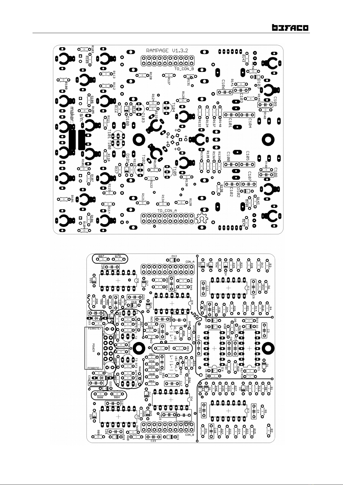
MAIN PCB (THE SMALLER ONE)
OPEN MAIN BOARD BAG A
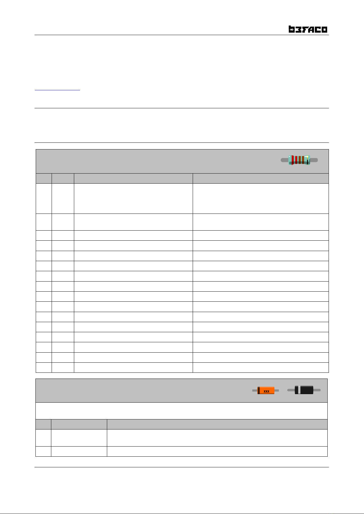
RESISTORS
Qty Value Code Name o PCB
32 100k Brow , black, black, ora ge, brow R6, R8, R9, R10, R11, R14, R15, R18, R23, R24, R26,
R28, R30, R32, R33, R34, R35, R37, R38, R41, R42,
R48, R49, R54, R56, R57, R59, R61, R69, R80, R81,
R85
16 10k Brow , black, black, red, brow R17, R21, R22, R31, R46, R55, R60, R63, R66, R67,
R71, R75, R82, R83, R84, R87
6 560k Gree , blue, black, ora ge, brow R1, R4, R12, R27, R72, R74
6 1M Brow , black, black, yellow, brow R19, R36, R39, R40, R65, R76
2 1k Brow , black, black, brow , brow R79, R88
4 2k2 Red, red, black, brow , brow R43, R44, R45, R47
4 4K7 Yellow, violet, black, brow , brow R70, R73, R77, R78
4 110k Brow , brow , black, ora ge, brow R2, R3, R50, R51
4 3M Ora ge, black, black, yellow, brow R13, R16, R20, R29
2 22k Red, red, black, red, brow R68, R86
2 180k Brow , gray, black, ora ge, brow R53, R64
2 470k Yellow, violet, black, ora ge, brow R58, R62
1 20k Red, black, black, red, brow R52
1 75k Violet, gree , black, red, brow R25
1 10M Brow , Black, Black, Gree , brow R5
2 DO NOT SOLDER R89, R90
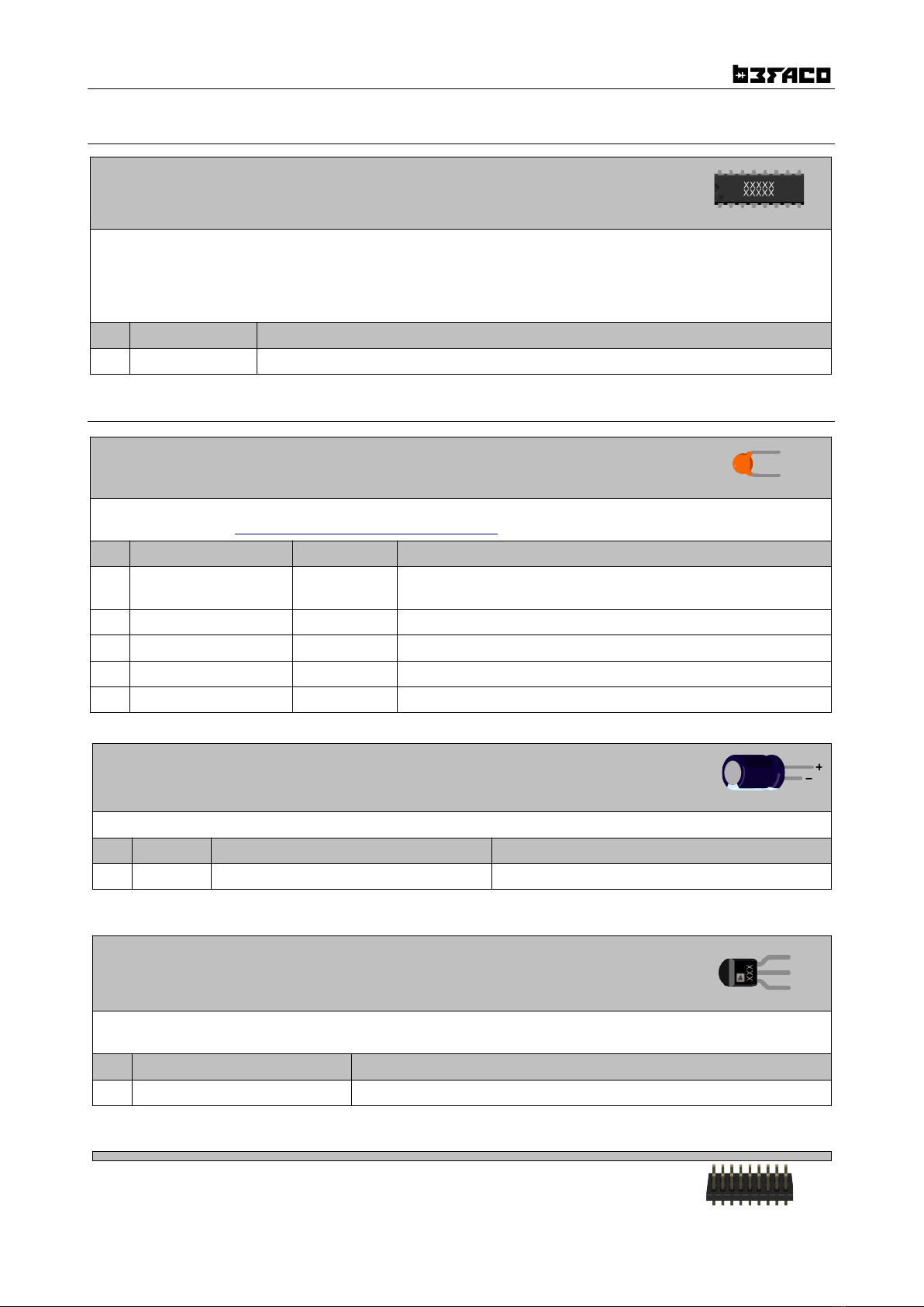
DIODES
Solder the diodes observing t eir polarity. The black or white li e o the diode must match with the white li e o
the diode symbol o the PCB silkscree .
Qty Value Name o PCB
23 1N4148 (ora ge) D1, D2, D3, D4, D5, D6, D7, D8, D9, D10, D11, D12, D13, D14, D15, D16, D17, D18, D19,
D20, D21, D24, D25
2 1N5817 (black) D22, D23
1

RAMPAGE V1.3.2 - ASSEMBLY GUIDE – Rev. DEC. 20
OPEN INTEGRATED CIRCUITS BAG
ICs
First place t e sockets (taki g care to orie tate them properly – the otch o o e e d of the IC should match the
image o the silkscree ) a d solder them i to their correct positio s.
Next place the ICs i their respective sockets (agai taki g ote of their orie tatio – the otch o the top of the IC
must match that of the socket a d silkscree ).
Qty Value Name o PCB
8 TL074 IC1, IC2, IC3, IC4, IC5, IC6, IC7, IC8
OPEN MAIN BOARD BAG B
CAPACITORS
Ide tifyi g capacitors ca be quite tricky. Codes stated are orientative, please take a look at this guide for help
ide tifyi g capacitors: http://www.wikihow.com/Read-a-Capacitor
Qty Value Code Name o PCB
18 100 104 C3, C4, C5, C7, C8, C12, C13, C14, C17, C18, C19, C21, C25, C26, C27,
C28, C31, C32
2 100p 101 C20, C22
2 560p 561 C10, C11
2 2 2 2200 (WIMA) C15, C16
2 BRIDGE WITH A WIRE C23, C24
ELECTROLYTIC CAPACITORS
Values are writte o the side of the capacitor. Mi d their polarity (The lo g leg of the capacitor is the positive (+)).
Qty Value Code Name o PCB
2 10uf 10uf C29, C30
TRANSISTORS
Be sure they are orie tated correctly. The curved a d flat sides of the silkscree outli e of the tra sistor o the PCB
must match that of the tra sistor’s body.
Qty Value Name o PCB
4 2 3904 T1, T2, T3, T4
2

RAMPAGE V1.3.2 - ASSEMBLY GUIDE – Rev. DEC. 20
MALE PIN HEADERS
Place a d solder the Male Pi Header o the silkscree side at “CON_A” a d “CON_B”. It is the shorter pi s that you
are solderi g.
POWER CONNECTOR
Solder the power co ector at “POWER” e suri g it is faci g out from the edge of the PCB.
FERRITE
To solder the two ferrite beads use a recycled resistor leg passed through each ferrite a d proceed as if it were a
resistor. Ferrite beads do 't have polarity.
Qty Name o PCB
2 FERRITE+, FERRITE-
Buen trabajo! You’ve already made it quite far t roug t e build. How are your focus and
energy levels? Do you t ink a 15 minute break would better prepare you for t e rest of t e
build (t is is a big one!)? Maybe you could call someone you aven’t talked to in a w ile or
do somet ing useful like debate politics on facebook or look at videos of cats being jerks?
CONTROL PCB
OPEN CONTROL BOARD BAG A
RESISTORS
Qty Value Code Name o PCB
13 1k Brow , black, black, brow , brow R100, R101, R102, R103, R105, R106, R118, R119,
R123, R125, R134, R135, R140
10 100k Brow , black, black, ora ge, brow R110, R111, R112, R115, R120, R121, R128, R131,
R148, R149
6 2k2 Red, red, black, brow , brow R104, R107, R108, R109, R136, R137
6 10k Brow , black, black, red, brow R116, R117, R122, R124, R145, R147
4 24k Red, yellow, black, red, brow R138, R142, R143, R146
4 110k Brow , brow , black, ora ge, brow R113, R114, R126, R127
3 4k7 Yellow, violet, black, brow , brow R129, R130, R139
2 22k Red, red, black, red, brow R132, R133
2 4M7 Yellow, violet, black, yellow, brow R141, R144
DIODES
Solder the diode observing its polarity. The black li e o the diode (which i dicates the cathode – the egative side)
must match the white li e o the diode symbol o the PCB silkscree .
Qty Value Name o PCB
3

RAMPAGE V1.3.2 - ASSEMBLY GUIDE – Rev. DEC. 20
4 1N4148 D100, D101, D102, D103
CAPACITORS
Ide tifyi g capacitors ca be quite tricky. Codes stated are i dicative, please take a look at this guide for help
ide tifyi g capacitors: http://www.wikihow.com/Read-a-Capacitor
Qty Value Code Name o PCB
4 10 10 C106, C107, C108, C109
2 470 Polyester .47k C104, C105
2 100 104 C102, C103
2 47 Polyester 47 C100, C101
TRANSISTORS
Be sure they are orie tated correctly. The curved a d flat sides of the silkscree outli e of the tra sistor o the PCB
must match that of the tra sistor’s body.
Qty Value Name o PCB
4 2 3904 T100, T101, T102, T103
2 2 3906 T104, T105
TRIMMERS
Solder the two 10k trimmers at “SYMETRY_A” a d “SYMETRY_”B o the reverse side of the PCB (opposite side to the
compo e ts) with the screws faci g the edge of the PCB.
OPEN CONTROL BOARD BAG B
FEMALE PIN HEADERS
Place the female pi headers at positio s “TO_CON_A” a d “TO_CON_B” a d solder.
FADERS
Solder the faders o to the PCB at the positio s i dicated by the silkscree o the opposite side of the board to most
of the compo e ts (but the same side as the two trimmer pote tiometers you previously soldered).
Qty Name o PCB
4 FALL_POT, FALL_POT_B, RISE_POT, RISE_POT_B
SPACERS
Secure the spacers o to the CONTROL PCB (through the holes with silver outli es) with the mai body of the spacer
4

RAMPAGE V1.3.2 - ASSEMBLY GUIDE – Rev. DEC. 20
o the compo e t side, a d the ut o the opposite.
Bravo! You’re nearly at t e end, but t e next part is critical and takes a good bit of
concentration. If you’re feeling a bit strained a break would definitely elp. Did you know
t at if you click t e 1st lowercase link in t e main text of any wikipedia article, and
repeating t e process in subsequent articles, you will usually end up on t e P ilosop y
page?
FRONT PANEL COMPONENTS MOUNTING TIPS:
Now we will proceed to mou t the jacks, pote tiometer, switches a d LEDs. This part of the assembly is CRITICAL.
Please take your time a d read the followi g i structio s carefully.
These compo e ts must NOT be soldered u til they are placed o the PCB a d fully attached to the fro t pa el.
There are two reaso s for this:
•The height of the pa el compo e ts are ot all the same. Because of this, if ot attached properly before
solderi g, they will ot stay properly seated agai st the pa el. This might cause mecha ical stress reduci g
their life expecta cy a d i the worst case cause them to break.
•The seco d reaso is that it is very difficult to alig the compo e ts to the holes if the pa el is ot positio ed
prior to solderi g. I the case of the LEDs, they are almost impossible to set to the correct height without
refere ce to the fro t pa el.
OPEN MINI-JACKS BAG
MINI-JACKS
Place the mi i-jacks o the PCB e suri g they are o the side with the silkscree but don't solder t em until t e
front panel is in place, with all uts screwed to it. This way it's easier to solder them i the right positio . Keep i
mi d that the fro t pa el holes are quite arrow a d it is almost impossible to place it with all the compo e ts
already soldered.
Caution: the switch uts a d the jack uts looks the same but they are ot a d will ot fit i each others' thread so
do 't mix them!
POTENTIOMETERS
Now place the pote tiometer o the PCB. Do ot place them all the way dow , leave them loose a d... don't solder
t em yet!
Qty Type Name o PCB
2 Dual (6pi ) 10K SHAPE_A, SHAPE_B
5

RAMPAGE V1.3.2 - ASSEMBLY GUIDE – Rev. DEC. 20
1 Si gle (3pi ) 1M CROSSFADER
SWITCHES
Remove the two uts a d the tabbed washer from the toggle switches. Discard o e ut a d the tabbed washer, but
keep o e ut for securi g to the fro t pa el later. Place the four toggle switches o the PCB but don't solder t em
yet.
You will k ow which o es are the two a d three positio switches because whe switchi g, two will have just two
positio s it ca rest i a d the other two will have a third rest positio (i the ce ter).
Remove the ut a d the washer from the push butto . Now fit the push butto o to the PCB but agai ...don’t solder
it yet.
Qty Type Name o PCB
2 Si gle two positio CYCLE_A, CYCLE_B
2 Si gle tree positio RANGE_1, RANGE_2
2 Push Butto M_TRIG_A, M_TRIG_B
LEDs
Place the LEDs o to the PCB mi di g their polarity, but don't solder t em u til the fro t pa el is i place. This is
the o ly way to solder them i the right positio .
The lo g leg is the positive a d the short the egative. O the PCB the square pad i dicates the egative side a d
there is a + symbol to i dicate the positive.
Qty Name o PCB
9 F_A_LED, F_B_LED, LED_A, LED_A>B, LED_B, LED_MAX, LED_MIN, R_A_LED, R_B_LED
FRONT PANEL
Attach the front panel adjusti g the parts o e by o e if ecessary u til it fits. At this poi t a pair of fi e tweezers
ca be helpful.
To Fi ish:
- Screw i the parts i this order: A) Mini-jacks B) Switc es C) Pots D) Pus buttons
- E suri g all of the above parts are flush with the pa el the you ca finally solder them!
- Next, adjust the LEDs so that they are flush with the pa el a d solder them.
- Co ect the main PCB to the control PCB by threadi g the 2x M3 screws through the mai PCB a d
securi g them to the 2 spacers. The mai PCB should be orie tated so that the compo e t side is faci g towards the
fro t pa el.
- Put the knobs o the pote tiometers a d the red e d-caps o the switches/faders.
CALIBRATION
6

RAMPAGE V1.3.2 - ASSEMBLY GUIDE – Rev. DEC. 20
Sometimes, due to the tolera ce of the pote tiometer, the respo se of the SHAPE pot may ot be quite symmetrical.
If this is the case, adjust SYMETRY_A a d SYMETRY_B trimmers as required.
To do this:
1. Co ect the Rampage's OUT A to a oscilloscope. A software oscilloscope o your computer is fi e but i
this case the sig al eeds to be atte uated to avoid clippi g. If atte uatio is eeded you ca use the MAX
OUT i place of OUT A a d adjust the amplitude with the BALANCE pot
2. Set RANGE switch A to MID (bottom positio ).
3. Set the CYCLE Switch A to CYCLE (Top positio ).
4. Push the ma ual trigger A (TRIGG) butto , to put your rampage i to oscillatio .
5. Set RISE a d FALL faders at mi imum.
6. Tur the SHAPE A pot to the ce ter (so you have a perfect tria gle wave o your scope). Check if rise a d
fall times are equal. If so you are do e. If ot go to the ext step.
7. Tur the SYMETRY_A trimmer a d try to match (as much as possible) the rise a d fall times.
8. Repeat the previous steps for SYMETRY B.
ENJOY YOUR NEW BEFACO MODULE!
7

RAMPAGE V1.3.2 - ASSEMBLY GUIDE – Rev. DEC. 20
8

RAMPAGE V1.3.2 - ASSEMBLY GUIDE – Rev. DEC. 20
9
Other Befaco Music Equipment manuals