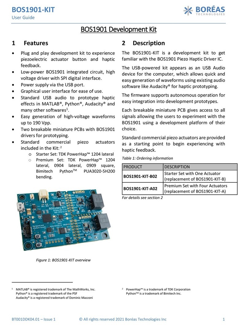
Boreas Technologies BOS1211 User manual

BOS1211-KIT CONFIDENTIAL
User Guide –Preliminary
BT002BDK01.05 –Issue 5 © All rights reserved 2020 Boréas Technologies Inc 1
BOS1211 Development Kit
1Features
•Plug and play development kit to experience
piezo haptic feedback
•Low-power BOS1211 integrated circuit, high
voltage driver with digital interface
•Easy generation of high-voltage waveforms
up to 120 V
•Enable sensing and emulate button behavior
using the actuator
•Three miniature PCB slots for scalable
BOS1211 driver boards
•Compatible with big piezoelectric actuators
such as TDK PowerHapTM
1
120 V models.
Figure 1: BOS1211-KIT Overview
2Description
The BOS1211-KIT is a Development Kit to help
users get familiar with the BOS1211 Piezo Haptic
Driver IC.
Miniature PCBs are interchangeable allowing the
users to experiment with the actuator sizes
adapted to their platform.
This kit connects to associated PC software over
USB for easy programming of the BOS1211 and
manual generation of waveforms on the
connected actuator.
The piezoelectric actuator sensing capability is
used to emulate a button behavior. The sensing
and feedback parameters can be changed using
the software.
Many GPIOs and hardware features are accessible
to ease prototype building.
Table 1: Ordering information
PRODUCT
DESCRIPTION
BOS1211-KIT-B
Starter Set with one actuator
For details see section 10.
1
PowerHap™ is a trademark of TDK Corporation.

BOS1211-KIT CONFIDENTIAL
User Guide –Preliminary
BT002BDK01.05 –Issue 5 © All rights reserved 2020 Boréas Technologies Inc 2
3Quick-Start Guide
3.1 What's in the Box
The content of the BOS1211-KIT is given in the following table.
Table 2: Starter Set BOS1211-KIT-B development kit content
#
ITEM
DESCRIPTION
REFERENCE
1
Controller board
BOS1211-BRD-C controller evaluation board.
2
Driver board - Small
BOS1211-BRD-S driver board for smaller actuators.
3
Driver board –
Medium
BOS1211-BRD-M driver board for medium actuators.
4
Driver board - Large
BOS1211-BRD-L driver board for larger actuators.
5
USB Cable Micro
Type B
USB communication cable to connect the
LaunchPadTM to a computer.
Stewart Connector part number SC-2AMK001F
6
3 terminal block
connectors
Male connector used for interfacing the piezoelectric
actuator on the driver boards.
Molex part number 39510-0002

BOS1211-KIT CONFIDENTIAL
User Guide –Preliminary
BT002BDK01.05 –Issue 5 © All rights reserved 2020 Boréas Technologies Inc 3
#
ITEM
DESCRIPTION
REFERENCE
7
TDK Piezo Actuator
TDK PowerHap™ 1919H021V120 (25G) Actuator
Ordering: Z63000Z2910Z 1Z43
Capacitance : 2.5 μF
Dim : 19.4 x 19.4 x 2.1 mm
8
12 V Power Supply
Power supply to provide 12 V to the Evaluation PCB.
CUI inc. part number SDI90-12-U-P5 with power chord
CUI inc. part number AC-C13 NA or equivalent.
9
Power adapter
European power adapter Ceptics model CT-9 or
equivalent

BOS1211-KIT CONFIDENTIAL
User Guide –Preliminary
BT002BDK01.05 –Issue 5 © All rights reserved 2020 Boréas Technologies Inc 4
3.2 Board Overview
Figure 2: BOS1211-KIT-BRD-C controller board
Figure 3: BOS1211-KIT-BRD-C controller board overview
USB
USR
RST
µC
www.boreas.ca
BOS1211-KI T-
BRD-C
D1
Debug
port
USBUSB
D2
Digital
Inputs Digital
Outputs
ADC &
DAC
Ext.
I2CM
External
SPI Master
SPI
sel.
Mount
hole
Mount
hole
Mount
hole
Mount
hole
BOS1211
Expansion
Port
Slot Card A
Slot Card B
Slot Card C
12V
connector
Level
shifter
array
SPI
switch
array
TP
12V
TP
GND
TP
VSPI
TP
5V
TP
GND
TP
3.3V
TP
GND
D3C
D3B
D3A

BOS1211-KIT CONFIDENTIAL
User Guide –Preliminary
BT002BDK01.05 –Issue 5 © All rights reserved 2020 Boréas Technologies Inc 5
3.3 Quick-Start Procedure
Important Note: this evaluation kit does not support hot swapping the driver boards in or out of the
controller board.
1. When shipped the BOS1211-KIT-BRD-C is already loaded with the appropriate firmware. If the
firmware needs updating, see section 5.4.
2. Install the PC GUI software. See section 6.1.
3. Launch the software application. See section 6.2.
4. Connect cables and the piezoelectric actuator. See section 4.1.
5. Select the appropriate USB Serial Device (COMxx) and click Connect to Port. See section 6.2.
6. Select parameters to play and click the Play button. Feel the feedback played on the actuator.
Warning: When measuring voltage signals on the actuator using an oscilloscope, use a separate probe
on each terminal of the actuator. Never connect the ground of a probe to one of these terminals. Doing
so might damage the BOS1211-KIT and/or your oscilloscope.

BOS1211-KIT CONFIDENTIAL
User Guide –Preliminary
BT002BDK01.05 –Issue 5 © All rights reserved 2020 Boréas Technologies Inc 6
4Hardware
4.1 Kit Assembly Overview
The kit is an assembly of many boards as shown in the figure below.
The larger BOS1211-KIT-BRD-C is the main controller board.
The smaller BOS1211-KIT-BRD-S, BOS1211-KIT-BRD-M and BOS1211-KIT-L driver boards must be inserted
in one of the three card sockets. They may be inserted in any order. Not all sockets need to be populated.
Use a terminal block to connect the actuator. Red wire must be connected at OUT pin, and black wire
must be connected at VIN pin. The provided terminal blocks are insertable in terminal block socket for
easy assembly and interchanging.
Connect the 12 V power supply to the controller board and connect the USB connector to a PC USB data
port to interface with the GUI software. It is possible to connect the USB cable to a USB charger port,
this limits the board behavior (see section 5.3.2).
Figure 4: BOS1211-KIT assembly overview

BOS1211-KIT CONFIDENTIAL
User Guide –Preliminary
BT002BDK01.05 –Issue 5 © All rights reserved 2020 Boréas Technologies Inc 7
4.2 Changing the Miniature Driver Boards
BOS1211 board components can be scaled depending on the piezoelectric actuator used. Each driver
board (BOS1211-KIT-BRD-S, BOS1211-KIT-BRD-M and BOS1211-KIT-L) has been designed with
components to support various actuator sizes. The table below indicates which driver board is best
suited depending on the actuator capacitance.
Table 3 Board revisions and compatible software
PART NUMBER
DESCRIPTION
MAX PIEZO ACTUATOR
CAPACITANCE
(for 300 Hz, 120 V waveforms*)
COMPATIBLE TDK
POWERHAPTM ACTUATORS
BOS1211-KIT-BRD-S
Small layout driver board
with lower drive.
Up to 0.9 µF
1313H018V120
BOS1211-KIT-BRD-M
Medium layout driver
board with medium drive.
Up to 2.5 µF
1919H021V120
BOS1211-KIT-BRD-L
Larger layout driver board
with higher drive.
Up to 4.4 µF
2626H023V120
6005H070V120
6005H090V120
*If the voltage and/or bandwidth are different, the maximum capacitance in your application can be
approximated with the following equation.
𝐶𝑚𝑎𝑥 = 𝐶𝑡𝑎𝑏𝑙𝑒 ∗300 𝐻𝑧
𝑓
𝑢𝑠𝑒𝑟
∗𝑉𝑡𝑎𝑏𝑙𝑒
2
𝑉
𝑢𝑠𝑒𝑟
2
Important Note: this evaluation kit does not support hot swapping the driver boards in or out of the
controller board.
Before changing driver boards, first disconnect both the USB cable and the 12 V supply. Then disconnect
the insertable terminal block joining the actuator. Change the driver boards for the desired
configuration, then successively reconnect the terminal blocks, the 12 V supply and the USB cable.
Although one of each driver board is included in the development kit, it is possible to get additional
driver boards as needed. Therefore, it is possible to connect many identical boards on the same
controller board.

BOS1211-KIT CONFIDENTIAL
User Guide –Preliminary
BT002BDK01.05 –Issue 5 © All rights reserved 2020 Boréas Technologies Inc 8
4.3 Identifying the Boards Revision Number
Each PCB board reference design and revision number (v#.#) are identified next to the “REF:” label. The
following table indicates compatibility with the firmware and Devkit Controller software.
Table 4 Compatible TDK PowerHapTM actuators for each driver board
REF NUMBER
COMPONENT
COMPATIBLE FIRMWARE
COMPATIBLE PC SOFTWARE
PCB-0069-BT002-DK-C-v1.1
BOS1211-KIT-BRD-C
Up to 1.7.x
Up to 2.7.x
PCB-0070-BT002-DK-S-v1.1
BOS1211-KIT-BRD-S
Up to 1.7.x
Up to 2.7.x
PCB-0070-BT002-DK-M-v1.1
BOS1211-KIT-BRD-M
PCB-0070-BT002-DK-L-v1.1
BOS1211-KIT-BRD-L
PCB-0089-BT002-DK-S-v1.3
BOS1211-KIT-BRD-S
Up to 1.7.x
Up to 2.7.x
PCB-0089-BT002-DK-M-v1.3
BOS1211-KIT-BRD-M
PCB-0089-BT002-DK-L-v1.3
BOS1211-KIT-BRD-L

BOS1211-KIT CONFIDENTIAL
User Guide –Preliminary
BT002BDK01.05 –Issue 5 © All rights reserved 2020 Boréas Technologies Inc 9
4.4 BOS1211-KIT-BRD-C Other Hardware
The controller board has additional hardware features to expand the board functionally when testing
actuators and building prototypes. These features are described in this section.
4.4.1 Probe Hooks
Probe hooks have been inserted around the board to ease connection of instruments for measurement
of supplies when debugging.
4.4.2 Expansion Port
An expansion port is available to provide test point access to the SPI I/Os. This port is labeled TPSPI in
the BOS1211-KIT-BRD-C schematics. It is initially unpopulated but can be using a Sullins Connector
Solutions model number SBH11-NBPC-D12-SM-BK or equivalent.
4.4.3 GPIO
General-purpose inputs and outputs are provided to easier integration of the development kit in a
prototype. For example, digital inputs may be used as trigger inputs to fire the waveforms or to send
information from the system to the development kit.
Using these GPIOs implies to modify the firmware to support them. However, they are already physically
implemented and routed to the MCU. They only need to be activated in the firmware software code
project.
There are 8 inputs and 8 outputs available on header connectors at the bottom of the board. A jumper
is initially shorting VIO-IN and VIO-OUT with the board 3.3 V pin so they are referenced to the board
main 3.3 V supply. To use an external supply, remove the jumpers and connect the external voltage
supply to the VIO-IN and VIO-OUT pins. The external supply must be in the 1.65 to 5.5 V range. VIO-IN
and VIO-OUT may have different supply levels.
Refer to the board schematics in section 7.1 for MCU pins numbers corresponding to the inputs and
outputs used.
4.4.4 ADC and DAC Connections
One DAC and four ADC pins are made available to the user. These connections are buffered to protect
the controller board. These signals cannot exceed the board 3.3 V supply level.
Using these implies to modify the firmware to support them. However, they are already physically
implemented and routed to the MCU. They need to be activated in the firmware software code project.
4.4.5 External SPI Master
All BOS1211 actuator driver chips are controlled via the SPI interface using the PSoC6 MCU as master. It
is, however, possible to bypass the MCU and use an external SPI master. This can be useful when trying
to connect the BOS1211 ICs directly to an external system.
SCK, MISO and MOSI connections are shared by all BOS1211 on the driver boards. Three chip selects
(CSA, CSB and CSC) are required to access the chip select pin on each BOS1211 in the slots A, B and C.
By default, a jumper on 5 V and VSPI forces the internal 5 V supply to be used. To use an external voltage
domain, remove this jumper and connect VSPI to the external supply.

BOS1211-KIT CONFIDENTIAL
User Guide –Preliminary
BT002BDK01.05 –Issue 5 © All rights reserved 2020 Boréas Technologies Inc 10
Finally, set the SPI Select switch to the EXT position to select the external SPI master, or leave it at the
INT position to use the MCU as the SPI master.
4.4.6 External I2C Master
Connections are provided to allow for an External I2C Master to be used. This is useful to connect the
controller board to a system that requires I2C connectivity.
Initially, this function is not implemented in the firmware. The firmware source code must be modified
for the MCU to act as an I2C slave. However, the board makes it possible if needed and allows for an
external voltage domain to be used as well.
By default, a jumper on 3.3 V and VI2C forces the internal 3.3 V supply to be used. To use an external
voltage domain, remove this jumper and connect VI2C to the external supply. Note only a 3.3 V or 5 V
supply may be used.
4.4.7 RST and USER Push Buttons
RST push button forces a reset of the MCU and the firmware.
USER is not used by the current firmware.
4.4.8 LED
A total of 5 LEDs are present on the development kit BOS1211-KIT-BRD-C board.
D1 (green LED) and D2 (red LED) are located near the USB connector. They indicate firmware revision
during boot up and provide information on development kit operation. See sections 5.1 and 5.2 for
details.
D3A, D3B and D3C (orange LED) are located next to their associated channel slot card and are used to
indicate that channel current status (see section 5.2).

BOS1211-KIT CONFIDENTIAL
User Guide –Preliminary
BT002BDK01.05 –Issue 5 © All rights reserved 2020 Boréas Technologies Inc 11
5Firmware
5.1 Identifying the Firmware Revision Number
When powering up the development kit, LEDs will show the firmware revision number and then the IC
revision.
After the 10-second bootload window while both LEDs are on (for firmware revisions below 1.5.0), the
green and red LEDs flash to indicate the firmware revision number. For a firmware revision X.Y.Z with
major revision X, minor revision Y and patch revision Z, the green LED will flash X times, then the red LED
will flash Y times and then both LEDs will flash Z times. The routine will execute twice. If no problem
were detected, the green LED will stay lit otherwise only the red LED will light up.
5.2 LED Indicators
The MCU continuously monitors the status of each channel. The status is then shown by the associated
LED (D3A, D3B, D3C). If an error occurs for a channel, the red LED (D2) will light up and the corresponding
channel orange LED will flash a number of times to indicate the error (see Table 5). The error will be
indicated in cycles until the issue is resolved. When no error is detected and a slot card is inserted, the
corresponding LED will stay lit.
Table 5: Channel LED flashing routine when in error
FLASHING
COUNT
ERROR DESCRIPTION (IC_STATUS FLAG)
0
No error.
1
Output voltage exceeded the maximum voltage allowed (OVV)
2
Overtemperature detected (OVT)
3
Maximum power reached; distortion is likely (MAX_POWER)
4
Problem with current detection (IDAC)
5
VDD too low (UVLO5)
6
VIN too low (UVLO12)
7
VIN too high (OVLO12)
8
Short-circuit detected between VOUT and VIN (SC)
For more information on the status error, please refer to the BOS1211 datasheet.
5.3 Modes of Operation
5.3.1 PC Connected
When the board is connected to a PC running the Boréas DevKit Controller software, it will communicate
with it and the user can control the board using the software interface.

BOS1211-KIT CONFIDENTIAL
User Guide –Preliminary
BT002BDK01.05 –Issue 5 © All rights reserved 2020 Boréas Technologies Inc 12
5.3.2 Persistence Mode
When booting the BOS1211-BRD-C evaluation board, the firmware will enter the Persistence mode. In
this mode, the board will behave as programmed by its internal memory. The memory can be set from
the PC software to a specific feedback waveform and trigger mechanism. When using the external
trigger, a rising edge on the GPIO input pin 0 will trigger the waveform stored in memory. If sensing was
activated when programming the memory, sensing will be activated in the Persistence mode.
When the Boréas DevKit Controller software is connected, any configuration push to the board will
override this Persistence mode. The Persistence mode can be restored by rebooting the board, either by
pressing the RST button or by unplugging the USB cable.
This mode will operate whether the board is connected to a PC USB port or a charger port.
5.4 Firmware Installation/Update Procedure
5.4.1 Kits Shipped with Firmware Revision Prior to 1.5.0
The BOS1211-KIT is provided out of the box with a firmware for use as USB Serial Device.
This firmware can be changed and/or updated using the dfuh-tool.exe application available on Boréas
website. The procedure is the following (refer to the figure below for each step):
1. Load the appropriate *.cyacd2 file using the browse button next to the file selection text box.
2. Click the “Filters…” button and make sure only “Show UART ports”is checked.
3. Set UART settings to:
a. baud rate : 115200
b. data bits : 8
c. stop bits : 1
d. parity : None
4. Press and release the "RST" button on the evaluation PCB to set it to Device Firmware Update
(DFU) mode. A new “USB Serial Device –UART”item should appear in the ports text box. Select
this port then press on the program button. Note that upon reset this port will be connected
for only 10 seconds. Programming must be done within that time.
5. Wait for installation/update to finish. The "Log" field will inform of a successful firmware
installation.
6. Once the installation is complete, LEDs will go through the firmware identification sequence
given in the previous section, and end with green LED on and red LED off. If red LED does not
turn off, wait a couple of seconds then press and release "RST" again.
Once the firmware has been updated to version 1.5.0 or later, it can then be updated to a future revision
using the procedure in the next section.

BOS1211-KIT CONFIDENTIAL
User Guide –Preliminary
BT002BDK01.05 –Issue 5 © All rights reserved 2020 Boréas Technologies Inc 13
Figure 5: dfuh-tool.exe for firmware installation/update
1
2
3
4
4
5

BOS1211-KIT CONFIDENTIAL
User Guide –Preliminary
BT002BDK01.05 –Issue 5 © All rights reserved 2020 Boréas Technologies Inc 14
5.4.2 Kits with Firmware Revision Installed is 1.5.0 or later
The following procedure applies to kits shipped with firmware revision 1.5.0 or later installed. It will also
apply to previous kits once the firmware has been updated to revision 1.5.0 or later.
When running the PC software, upon connecting the kit to the software, if the firmware revision
detected on the board is not compatible with the current software, the user will be asked if he wants to
update the firmware or not.
After clicking Yes, the firmware update will be updated automatically.
Figure 6: Firmware update request window

BOS1211-KIT CONFIDENTIAL
User Guide –Preliminary
BT002BDK01.05 –Issue 5 © All rights reserved 2020 Boréas Technologies Inc 15
6Boréas DevKit Controller PC Software
This User Guide is applicable to Boréas DevKit Controller software revisions starting with 2.7.x.
6.1 Installation
6.1.1 Software Installation
To install this application, please run the Boréas DevKit Controller installer executable file (Boreas-Dev-
Kit-Installer-2.7.x.exe). Follow the instructions given by the software. A shortcut on the desktop will be
created at the end of the installation.
6.1.2 Software Update
To update the application, download the latest installer and run it. The older version will automatically
be overwritten.
6.2 Using the Application
6.2.1 Overview
Boréas DevKit Controller is a graphical user interface (GUI) intended to ease evaluation of the BOS1211
IC. Using this application, users can easily trigger waveforms manually or using a system I/O, activate
sensing and monitor the IC state.
The following sections details the interface elements and how to use them.
6.2.2 Main Window
The main application window is separated into these sections:
1. Left panel
2. Mini-boards identification bar
3. Content tabs
When the board is not connected, only the left panel is visible.
Once the connection is established, the right panel will appear.
6.2.3 Left Panel
The left panel contains buttons that are always accessible. The upper section indicates the firmware of
the currently connected board.
USB Serial Device Dropdown List
This control lists the COM ports currently connected to the computer. The development board will
appear as a USB Serial Device with a dedicated COMxx name given by the system. Look for the one
appearing when physically connecting the board to know which label corresponds the board. Note the
board will also appear as a COM port during the initial bootloading sequence. Please wait for the green
LED before connecting to the board.
Connect to port/Disconnect from port
Once the appropriate port has been selected, click Connect to port to establish the communication with
the development board. Click Disconnect from port before unplugging the board. If the firmware revision

BOS1211-KIT CONFIDENTIAL
User Guide –Preliminary
BT002BDK01.05 –Issue 5 © All rights reserved 2020 Boréas Technologies Inc 16
is not compatible with the PC software, the user will have the opportunity to automatically update the
firmware.
About
This button opens the About box giving information about the application.
Exit
This button closes the application.
Figure 7 Main application window when not connected
6.2.4 Mini-boards identification bar
The top of the right panel provides information about the mini-boards connected to the controller
board. For each of the mini-boards inserted in slots A, B and C, the associated chip ID will appear. Slots
used will be marked as Connected, unused slots are indicated as Not connected.

BOS1211-KIT CONFIDENTIAL
User Guide –Preliminary
BT002BDK01.05 –Issue 5 © All rights reserved 2020 Boréas Technologies Inc 17
6.2.5 Basic Tab
For the selected mini-board tab, the Basic tab is used to send waveforms to the evaluation board. This
section describes each parameter and control.
Sync/Desync All Button
When pressed, all connected boards will play the same waveform using BOS1211 SYNC feature.
Depress the button to play waveforms on individual boards.
Save in Memory
This button will save the current configuration to the MCU internal memory. This configuration will be
automatically loaded when the board is booted, whether it is connected to a USB port or USB charger.
See Persistence mode at section 5.3.2.
Load from Memory
This button will load the Persistence mode configuration from the MCU internal memory.
Reset
Press the red reset button to return parameters in the board memory to their default values.
Amplitude
This value is the amplitude in volt of the waveform played. The waveform will be played between 0 V
and this value. Value is valid between 20 and 120 V.
Frequency
This value is the frequency in Hertz of the waveform played. Value is valid between 100 and 300 Hz.
Cycle
This value is the number of sine cycles played. The minimum valid value is 1 cycle. The maximum value
when playing half-waves is 10 cycles. The maximum value when playing full sine waves is 16711425.
Stabilization Time
This value determines the time the piezo creep will be stabilized after playing a waveform. The valid
range is from 0 to 1000 ms.
Half-Wave
When unchecked, each waveform cycle will correspond to a full sine cycle (0 to 2π).
When checked, each waveform cycle will correspond a sine half-cycle (0 to π).
Play Button
This button manually triggers a waveform to be played as defined by the above parameters.
Enable GPIO Interrupt
When checked, a pulse on GPIO input pin 0 will trigger the waveform as defined by the above
parameters. The pulse is debounced by the firmware. Its width must be at least 5 ms. Note that the
parameters must have been sent from the GUI to the device first.

BOS1211-KIT CONFIDENTIAL
User Guide –Preliminary
BT002BDK01.05 –Issue 5 © All rights reserved 2020 Boréas Technologies Inc 18
Figure 8 Main application window when connected - Basic tab
Sensing
When checked, the actuator will behave like a button, playing the waveform when pressed and released.
The release waveform amplitude is set to 75% of the press waveform amplitude. This box must first be
checked to adjust the sensing parameters.
Piezo Config
Selecting a specific piezoelectric actuator PowerHapTM model sets the default parameter profile for this
actuator. Individual parameters can then be adjusted.
Press/Release Settings
Sensing parameters are set separately for the press and release detection events.
Threshold
Value the piezo voltage must be over or below for a detection to be successful. Using TDK PowerHapTM
actuators, the threshold of a press event should be positive and that of a release event should be
negative.
Hold Time
Time the voltage must be above or below the threshold for the detection to be successful.

BOS1211-KIT CONFIDENTIAL
User Guide –Preliminary
BT002BDK01.05 –Issue 5 © All rights reserved 2020 Boréas Technologies Inc 19
Direction
Direction the voltage is crossing the threshold for a detection to be successful. Using TDK PowerHapTM
actuators, the direction of a press event should be upward and that of a release event should be
downward.
Figure 9 Main application window when connected - Basic tab - Sensing

BOS1211-KIT CONFIDENTIAL
User Guide –Preliminary
BT002BDK01.05 –Issue 5 © All rights reserved 2020 Boréas Technologies Inc 20
6.2.6 Registers Tab
The Registers Tab allows to monitor the register content of the selected connected mini-board. It also
allows to write specific values to any writeable registers on the driver IC by clicking the Send button next
to that register. Before editing any register, it is recommended to first click Load All. Be aware data will
be overwritten on the IC, even if not previously loaded.
The registers are displayed, one per line. The register label is given on the left, then the register address,
then the parameters for this register are given (MSB on the left, LSB on the right), and then there is Send
button to send the parameter values to the board IC if the register is writeable. When using this button,
and only the associated register for the selected channel is written.
When selecting a parameter box, the information for that parameter is given on the right side of the
screen. Information includes parameter name, its current value, the number of bits of that parameter
(Length), the minimum and maximum possible values, and a short description.
Figure 10 Main application window when connected - Registers tab
Table of contents
Other Boreas Technologies Microcontroller manuals
Popular Microcontroller manuals by other brands
Atmel
Atmel AVR2103 quick start guide
mikroElektronika
mikroElektronika CLICKER2 FOR PIC32MX manual

Renesas
Renesas mPD179327 Subseries user manual

Toshiba
Toshiba TLCS-870/C1 Series manual

Littelfuse
Littelfuse Zilog Z8 Encore! XP F3224 Series user manual

Texas Instruments
Texas Instruments MSP430FG461x series manual

