Brainboxes AD-593 User manual

2.1 EDITION Feb 1995
da
1200Series

PC AD1200 Reference
Thank You For Buying
PC AD1200
Interface!
We proudly present the PC AD1200 Interface Board.
The PC AD1200 Interface allows the PC user to measure
and control ’Real World’ analogue signals. AD1200 is 100%
compatible with the widely available DT2811 card and yet has
features that surpass and out perform that product. Blending the
discrete digital domain of computers with the infinitely variable
Analogue realm brings great power to the user, allowing control
and monitoring of almost any process. AD1200’s mix of high
performance Analogue to Digital input, Digital to Analogue
output, Digital input and Digital output hardware with a fully
functioned software package provides a straight forward route to
excellence in signal acquisition. Extend your grasp with AD1200.
Your board is designed and manufactured in England, and
our policy is one of complete support to our dealers and direct
to our users. Please note, PC AD1200 is designed ’in house’ and
is completely understood by our staff. Its great strength is the
software support we give it. Our intention is to supply the
software and any technical information you may need to allow
you to exercise complete control over the AD1200 board and
software. After searching the manuals, do not hesitate to contact
us on our HOTLINE numbers given on Intro Page-2, if you
need help.
We are particularly keen to provide new operating system
or language drivers to expand the range of applications using our
PC AD1200 board.
We trust that if you adhere to the following procedures you
will enjoy many years of useful service from your AD1200 card.
Intro-3

PC AD1200 Reference
PC AD1200 MANUAL____________________
The Layout Of This Manual._________________________
This manual is a complete description of how to install,
configure and use the PC AD1200 interface board.
The PC AD1200 card, like our other PC add on boards, is
an extremely easy to use and understand implementation of
Analogue interfacing for IBM PC and compatible computers. We
have truly tamed the Analogue world and the PC BUS allowing
you to get the most out of your data acquisition system!
Chapter 1, Introduction To The Analogue
World, describes the features of the range of AD1200 cards,
discusses the fundamentals of Analogue to Digital conversion,
Digital to Analogue conversion and explains exactly how the
AD1200 range implements these. Downwards compatibility with
the DT2811 is discussed as well as the extra high performance
features that distinguish the AD1200 range, this improved design
whilst retaining exact compatibility with other manufacturers
products gives AD1200 extreme flexibility in its application and
use. Converter throughput, interrupt and DMA driven i/o are
explained together with a complete description of the AD1200’s
timing and control modes.
Chapter 2, Installation Guide, shows you how to
configure and install the PC AD1200 board in one of the
expansion slots of your computer and gives the default setting of
all configurable options. All settings for I/O base address, IRQ
and DMA channels, ADC and DAC voltage ranges are shown.
Details of how to connect up the AD1200 to the users system
are given.
Intro-4

PC AD1200 Reference
Chapter 3, The AD1200 Register Map, details the
programmable status and control registers on the card. Whilst
most users will use the bundled driver software and so find this
information be be unnecessary it is included to make this manual
as complete as possible, to allow you to cover every eventuality.
Chapter 4, Calibration, shows how to perform a
calibration of the AD1200 analogue circuitry. The use of the
calibration software, the position and function of the onboard
trimmer pots and use of ancillary equipment are all described.
Calibration should be performed at regular intervals to ensure
that the AD1200 remains in specification, and that your analogue
measurements are traceable back to nationally and internationally
recognised standards.
Chapter 5, Technical Specification, gives the
complete technical specification on the AD1200 series of cards.
The Cumulative Index covers the complete contents of
the manual.
Intro-5

PC AD1200 Reference
Outline Contents.________________
Chapter 1. Introduction To The Analogue World.
Chapter 2. Installation Guide.
Chapter 3. The AD1200 Register Map.
Chapter 4. Calibration.
Chapter 5. Technical Specification.
Cumulative Index.
Chapter 1 Introduction To The Analogue World.___________________________________________
Introduction. 1
The PC AD1200 Range Of Cards. 2
From AD1221 Up To AD1200. 3
DT2811 Superset. 4
Introduction To Analogue. 5
Unipolar Vs Bipolar Voltage Ranges. 8
Differential Vs Single Ended Signals. 8
The Analogue To Digital Converter. 9
Input Channel Selection. 10
Programmable Gain. 11
Analogue Input Ranges. 11
Programmed I/O, Interrupts and DMA. 12
Programmed I/O. 12
Interrupt Driven I/O. 12
DMA, Direct Memory Access. 13
The Pacer Clock. 13
A/D Throughput and Pipelining. 14
A/D Operating Modes. 16
A/D Modes 0, 1, 2 & 3. 17
Mode 0, Single Conversions. 17
Mode 1, Continuous Conversions, Int Trig & Clock. 18
Mode 2, Continuous Conversions, Ext Trig Int Clk. 18
Mode 3, Continuous Conversions, Ext Trig & Clock. 19
The Analogue To Digital Converter. 20
D/A Programmed I/O. 20
Intro-6

PC AD1200 Reference
D/A Interrupts and DMA. AD1200 Card Only. 20
Digital I/O Ports. 21
Digital Port Programmed I/O. 21
Digital Port Interrupts and DMA. AD1200 Only. 21
Screw Terminal Board. 22
4-20mA Current Conversion Options. 23
Chapter 1 List Of Figures._______________________
Figure 1-1. AD1200 Series Common Properties. 2
Figure 1-2. AD1200 Series Options. 3
Figure 1-3. AD1200 card Vs DT2811. 5
Figure 1-4. One Bit A/D Conversion. 6
Figure 1-5. Two Bit A/D Conversion. 6
Figure 1-6. Three Bit A/D Conversion. 7
Figure 1-7. Bit Weights And Resolution. 8
Figure 1-8. Mode 0 & 1 Bits. 16
Figure 1-9. Extended Mode Bits. 17
Chapter 2 Installation Guide.__________________________
Introduction. 24
Configuring The PC AD1200 Board. 24
Setting The PC AD1200 I/O Address. 26
Using More Than One PC AD1200 Board. 33
Interrupt Selection. 33
Setting The Interrupt Jumper Block. 34
DMA Selection. AD1200 Only. 35
Setting The DMA Channel Jumper Block. 36
D/A Output Range Selection. 37
A/D Configuration. 38
8254 Counter Timer Pinouts. 43
Installing The PC AD1200 Board In The Computer. 44
AD1200 Backplane Signals. 46
Signal Types. 47
Wiring Guidelines. 49
Twisted Pair Cables. 49
Intro-7

PC AD1200 Reference
Shielded Cables. 49
Input Voltage. Overvoltage Warning! 50
Problems! 50
Chapter 2 List Of Figures._______________________
Figure 2-1. AD1200 Card Layout. 25
Figure 2-2. AD1210 AD1211 Card Layout. 26
Figure 2-3. AD1220 AD1221 Card Layout. 26
Figure 2-4a. AD1200 Factory Set DIP Switches. 27
Figure 2-4b. AD1210-21 Factory Set DIP Switches. 28
Figure 2-5. I/O Addresses To Avoid. 28
Figure 2-6. Likely I/O Address. 29
Figure 2-7a. AD1200 Base Addresses. 29
Figure 2-7b. AD1210-21 Base Addresses. 31
Figure 2-8. The IRQ Jumper Block. 35
Figure 2-9. The DMA Jumper Block. 37
Figure 2-11. A/D Channel Input Select. 39
Figure 2-12. AD1200 A/D Input Range Selection. 40
Figure 2-13. AD1210 A/D Input Range Selection. 41
Figure 2-14. AD1220 A/D Input Range Selection. 42
Figure 2-15. OUT0 Via Digital Input Bit 7, Pin36. 43
Figure 2-16. Remove Cover Mounting Screws. 44
Figure 2-17. Removing The PC Cover. 44
Figure 2-18. Removing Blanking Cover. 45
Figure 2-19. Inserting The PC AD1200 Card. 45
Figure 2-20. AD1200 J2 Pin Outs. 46
Chapter 3 AD1200 Register Map._____________________________
Introduction. 51
I/O Address Map. 51
Register Types. 52
Read Write Assignments. 52
Power Up Conditions. 53
The A/D Control Status Register. 53
Bit 7 A/D Done, Read Only. 53
Bit 6 A/D Error, Read Only. 54
Intro-8

PC AD1200 Reference
Bit 5 A/D Busy, Read Only. 54
Bit 4 Clear A/D Error, Write Only. 54
Bit 3 DMA Enable, Read / Write. AD1200 Only 54
Bit 2 Interrupt Enable, Read / Write. 55
Bits 0 & 1. Mode Bit 0 & 1. Read / Write. 56
Initialising The A/D Converter. 57
The A/D Gain Channel Register. 58
Bits 6 & 7. Gain select. Read / Write. 58
Bits 4 & 5. Reserved For Future Expansion. R/W. 59
Bits 0, 1, 2 & 3. Channel Select. Read / Write. 59
The A/D Converter Input Registers. Read Only 60
The DAC0 D/A Converter Output Registers. 62
The DAC1 D/A Converter Output Registers. 63
The Digital Output Port Register. Write Only 65
The Digital Input Port Register. Read Only 66
The Timer & Extended Mode Register. Read/ Write 66
Bits 0-5, TIMER Pacer Clock Divisor Bits. R/W. 67
Bits 6 & 7 XMODE, Extended Mode Read/Write. 69
The 8254 Counter Timer Registers. Read/ Write 70
Chapter 3 List Of Figures._______________________
Figure 3-1. AD1200 Register Map. 51
Figure 3-2. A/D Control Status Register. 53
Figure 3-3. Mode 0 & 1 Bits. 56
Figure 3-4. AD1200 Extended Mode Bits. 57
Figure 3-5. AD1210-21 Extended Mode Bit. 57
Figure 3-6. A/D Gain Channel Register. 58
Figure 3-7. Gain Selection. 59
Figure 3-8. Channel Selection. 60
Figure 3-9. ADC Low Byte Input Register. 61
Figure 3-10. ADC High Byte Input Register. 62
Figure 3-11. DAC0 Low Byte Output Register. 63
Figure 3-12. DAC0 High Byte Output Register. 63
Figure 3-13. DAC1 Low Byte Output Register. 65
Intro-9

PC AD1200 Reference
Figure 3-14. DAC1 High Byte Output Register. 65
Figure 3-15. DIGOUT Output Register. 65
Figure 3-16. DIGIN Output Register. 66
Figure 3-17. TIMEREX Register. 67
Figure 3-18. Pacer Clock Divisor 68
Figure 3-19. AD1200 Extended Mode Bits. 70
Figure 3-20. AD1210-21 Extended Mode Bit. 70
Figure 3-21. 8254 Counter Timer Register Map. 71
Chapter 4 Calibration.____________________
Introduction. 72
Calibrating The Digital To Analogue Output. 72
Outline. 73
Equipment Required. 73
DAC0 Calibration Procedure. 74
DAC1 Calibration Procedure. 75
Calibrating The Analogue To Digital Input. 77
Outline. 77
Equipment Required. 78
ADC Calibration Procedure. 78
Chapter 4 List Of Figures._______________________
Figure 4-1. DAC Trimmer Pot Layout. 73
Figure 4-2. DAC0 Calibration Wiring Diagram. 75
Figure 4-3. DAC Calibration Values. 75
Figure 4-4. DAC1 Calibration Wiring Diagram. 76
Figure 4-5. ADC Trimmer Pot Layout. 77
Figure 4-6. ADC Calibration Wiring Diagram. 78
Figure 4-7. Unipolar ADC Calibration Values. 79
Figure 4-8. Bipolar ADC Calibration Values. 80
Chapter 5 Technical Specification.______________________________
Introduction. 81
Analogue Inputs. 81
Analog Outputs 82
Digital I/O 82
Pacer Clock. 83
Power Consumption. 83
Intro-10

Introduction AD1200 Reference
CHAPTER 1
INTRODUCTION TO
THE ANALOGUE
WORLD.
Introduction.____________
This chapter describes the features of the range of AD1200
cards highlighting the differences between them, discusses the
fundamentals of Analogue to Digital conversion, Digital to
Analogue conversion and explains exactly how the AD1200
range implements these.
Downwards compatibility with the DT2811 is discussed as
well as the extra high performance features that distinguish the
AD1200 range, this improved design whilst retaining exact
compatibility with other manufacturers products gives AD1200
extreme flexibility in its application and use.
Converter throughput, Programmable Gain input, interrupt
and DMA driven i/o are explained together with a complete
description of the AD1200’s timing and control modes.
Note that throughout this manual reference is made to the
AD1200 series as either AD1200 series or as AD12XX card,
meaning that this information is common to all cards in the
AD1200 family.
When AD1210, AD1211, AD1220, AD1221 or the term
’AD1200 card’ the information is specific to those particular
cards mentioned.
Chapter 1 Page 1

AD1200 Reference Introduction
The PC AD1200 Range Of Cards._____________________________
The AD1200 series is a family of 12 bit analogue interface
cards. Currently 6 different cards are available. Each card has all
the base features of the range, the distinguishing features of each
card being variations in A/D throughput, Programmable Gain
ranges and DMA capabilities.
Figure 1-1. AD1200 Series Common Properties._________________________________________
Analog Input: 12 bit
Channels Type: 16 Single Ended
(jumper OR 8 Differential
selectable) OR 16 Pseudo Diff
Channel Select Programmable
Bipolar Input: ±10Volt, ±5Volt, ±2.5Volt
Unipolar Input: 0~10Volt, 0~5Volt
Interrupts
A/D Done IRQs: Yes
Analog Output: Two 12 bit DACs
Bipolar Output: ±10V, ±5V, ±2.5V
Unipolar Output: 0~10Volt, 0~5Volt
Throughput: 100kHz per DAC
Digital I/O
TTL output: 8 bit
TTL input: 8 bit
Throughput: 1MHz
Pacer Clock 0.005Hz-600kHz
External Clock: Yes (to 1Mhz)
External Trigger: Yes (-ve edge).
The common features of the AD1200 range are comprehensive
and sophisticated enough to make even the AD1221 a complete
data acquisition system on a single plug in board.
Page 2 Chapter 1
Introduction AD1200 Reference
Figure 1-2. AD1200 Series Options._______________________________
ÚÄÄÄÄÄÄÄÄÄÄÄÄÄÄÄÄÄÄÂÄÄÄÄÄÄÄÂÄÄÄÄÄÄÄÂÄÄÄÄÄÄÄÂÄÄÄÄÄÄÄÂÄÄÄÄÄÄÄ¿
³
Card
³
AD1221
³
AD1220
³
AD1211
³
AD1210
³
AD1200
³
ÃÄÄÄÄÄÄÄÄÄÄÄÄÄÄÄÄÄÄÅÄÄÄÄÄÄÄÅÄÄÄÄÄÄÄÅÄÄÄÄÄÄÄÅÄÄÄÄÄÄÄÅÄÄÄÄÄÄÄ´
³
A/D Throughput.
³
³
³
³
³
³
³
30kHz:
³
AD1221
³
³
AD1211
³
³
³
³
100kHz:
³
³
AD1220
³
³
AD1210
³
AD120
³
ÃÄÄÄÄÄÄÄÄÄÄÄÄÄÄÄÄÄÄÁÄÄÄÄÄÄÄÁÄÄÄÄÄÄÄÁÄÄÄÄÄÄÄÁÄÄÄÄÄÄÄÁÄÄÄÄÄÄÄ´
³
Programmable Gain Input.
³
ÃÄÄÄÄÄÄÄÄÄÄÄÄÄÄÄÄÄÄÂÄÄÄÄÄÄÄÂÄÄÄÄÄÄÄÂÄÄÄÄÄÄÄÂÄÄÄÄÄÄÄÂÄÄÄÄÄÄÄ´
³
None:
³
AD1221
³
AD1220
³
³
³
³
³
1-2-4-8:
³
³
³
AD1211H
³
AD1210H
³
AD1200H
³
³
1-10-100-1000:
³
³
³
AD1211L
³
AD1210L
³
AD1200L
³
ÃÄÄÄÄÄÄÄÄÄÄÄÄÄÄÄÄÄÄÁÄÄÄÄÄÄÄÁÄÄÄÄÄÄÄÁÄÄÄÄÄÄÄÁÄÄÄÄÄÄÄÁÄÄÄÄÄÄÄ´
³
DMA Capabilities.
³
ÃÄÄÄÄÄÄÄÄÄÄÄÄÄÄÄÄÄÄÂÄÄÄÄÄÄÄÂÄÄÄÄÄÄÄÂÄÄÄÄÄÄÄÂÄÄÄÄÄÄÄÂÄÄÄÄÄÄÄ´
³
None:
³
AD1221
³
AD1220
³
AD1211
³
AD1210
³
³
³
A/D Done:
³
³
³
³
³
AD1200
³
ÃÄÄÄÄÄÄÄÄÄÄÄÄÄÄÄÄÄÄÁÄÄÄÄÄÄÄÁÄÄÄÄÄÄÄÁÄÄÄÄÄÄÄÁÄÄÄÄÄÄÄÁÄÄÄÄÄÄÄ´
³
Pacer Clocked DMA.
³
ÃÄÄÄÄÄÄÄÄÄÄÄÄÄÄÄÄÄÄÂÄÄÄÄÄÄÄÂÄÄÄÄÄÄÄÂÄÄÄÄÄÄÄÂÄÄÄÄÄÄÄÂÄÄÄÄÄÄÄ´
³
DAC0 Output:
³
³
³
³
³
AD1200
³
³
DAC1 Output:
³
³
³
³
³
AD1200
³
³
DIG Output:
³
³
³
³
³
AD1200
³
³
DIG Input:
³
³
³
³
³
AD1200
³
ÀÄÄÄÄÄÄÄÄÄÄÄÄÄÄÄÄÄÄÁÄÄÄÄÄÄÄÁÄÄÄÄÄÄÄÁÄÄÄÄÄÄÄÁÄÄÄÄÄÄÄÁÄÄÄÄÄÄÄÙ
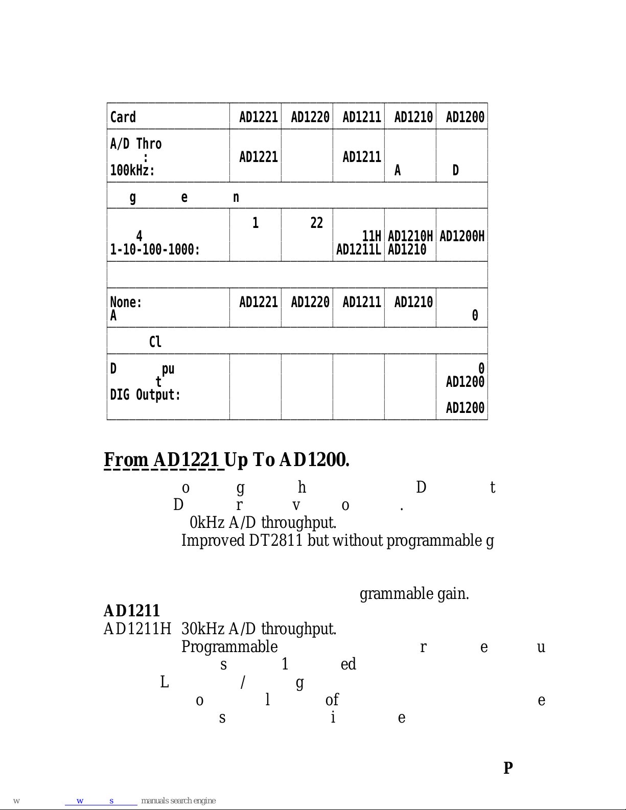
From AD1221 Up To AD1200.__________________________
So progressing from the entry level AD1221 to the fully
featured AD1200 card we have the following.
AD1221 30kHz A/D throughput.
Improved DT2811 but without programmable gain.
AD1220 100kHz A/D through put.
Faster DT2811 without programmable gain.
AD1211
AD1211H 30kHz A/D throughput.
Programmable Gain of 1-2-4-8 for High level input
signals. DT2811 improved equivalent.
AD1211L 30kHz A/D throughput.
Programmable Gain of 1-10-100-1000 for Low level
input signals. DT2811 improved equivalent
Chapter 1 Page 3

AD1200 Reference Introduction
AD1210
AD1210H 100kHz A/D throughput.
Programmable Gain of 1-2-4-8 for High level input
signals. Faster DT2811 improved equivalent.
AD1210L 100kHz A/D throughput.
Programmable Gain of 1-10-100-1000 for Low level
input signals. Faster DT2811 improved equivalent.
AD1200
AD1200H DMA input from A/D converter or Digital Input port.
DMA output to D/A converter or Digital Output port.
100kHz A/D through put.
Programmable Gain of 1-2-4-8 for High level input
signals. The ultimate 12 bit data acquisition system.
AD1200L DMA input from A/D converter or Digital Input port.
DMA output to D/A converter or Digital Output port.
100kHz A/D through put.
Programmable Gain of 1-10-100-1000 for Low level
input signals. The ultimate 12 bit data acquisition
system.
DT2811 Superset.________________
The Ad1200 series of cards are a great improvement on
the DT2811 specification, they have wider input and output
ranges, faster settling and acquistion times, greater throughput
and DMA capabilities.
Page 4 Chapter 1

Introduction AD1200 Reference
Figure 1-3. AD1200 card Vs DT2811.________________________________
Feature AD1200 DT2811
Analog Input:
Bipolar Input: ±10V, ±5V, ±2.5V ±5Volt, ±2.5Volt
Unipolar Input: 0~10Volt, 0~5Volt 0~5Volt
Throughput:
Gains 1 - 10 100kHz 20kHz
Gain 100 100kHz 2.5kHz
Gain 1000 80kHz 2.5kHz
Analog Output:
Bipolar Output: ±10V, ±5V, ±2.5V ±5V, ±2.5V
Unipolar Output: 0~10Volt, 0~5Volt 0~5Volt
Throughput: 100kHz per DAC 50kHz per DAC
Programmable Gain
Maximum Gain: 1000 500
Interrupts
A/D Done Interrupt Yes Yes
DAC0 Interrupt Yes No
DAC1 Interrupt Yes No
Digital In Interrupt Yes No
Digital Out Interrupt Yes No
DMA
A/D Done DMA: Yes No
DAC0 DMA Yes No
DAC1 DMA Yes No
Digital In DMA Yes No
Digital Out DMA Yes No
Introduction To Analogue._______________________
Analogue signals are things with which we are all familiar.
The intensity of the light reaching our eyes, the volume of the
sound in our ears, the temperature of the air in the room around
us are all analogue values. That is the light intensity may vary
continuously and smoothly from utter darkness to broad daylight.
Our senses are able to easily discriminate between many subtle
Chapter 1 Page 5

AD1200 Reference Introduction
levels of illumination. This is not so with computers.
A computer uses numbers to represent physical quantities,
storing the values using bit patterns. Each bit in a computer’s
memory is either off or on, it cannot be half way on or nearly
on. If we are to store the value of light intensity on a computer
there must be some method of turning the smoothly varying real
signal value into a bit pattern in the computers memory. This
process is called analogue to digital conversion.
If only one bit is to be used to represent the light intensity
then the illumination would be divided into either on or off.
From total darkness to half light would be off, half light to full
illumination would be on. One bit gives two illumination states.
In general terms, resolution means separation into components.
The resolution of a converter is the smallest interval measurable
by the converter and this one bit converter’s resolution is 50%
of the signal.
Figure 1-4. One Bit A/D Conversion.________________________________
ÚÄÄÄÄÄÄÄÄÄÄÄÄÄÂÄÄÄÄÄÄÄÄÄÄÄÄÄÄÄÄÄÄÄÄ¿
³
BIT PATTERN
³
ILLUMINATION LEVEL
³
ÃÄÄÄÄÄÄÄÄÄÄÄÄÄÅÄÄÄÄÄÄÄÄÄÄÄÄÄÄÄÄÄÄÄÄ´
³
1
³
ON
³
³
0
³
OFF
³
ÀÄÄÄÄÄÄÄÄÄÄÄÄÄÁÄÄÄÄÄÄÄÄÄÄÄÄÄÄÄÄÄÄÄÄÙ
If two bits of computer memory are used to represent the
light intensity then the illumination would be divided into off,
dark grey, light grey and full illumination. Two bits gives four
illumination states.
Figure 1-5. Two Bit A/D Conversion.________________________________
ÚÄÄÄÄÄÄÄÄÄÄÄÄÄÂÄÄÄÄÄÄÄÄÄÄÄÄÄÄÄÄÄÄÄÄ¿
³
BIT PATTERN
³
ILLUMINATION LEVEL
³
ÃÄÄÄÄÄÄÄÄÄÄÄÄÄÅÄÄÄÄÄÄÄÄÄÄÄÄÄÄÄÄÄÄÄÄ´
³
11
³
ON
³
³
10
³
LIGHT GREY
³
³
01
³
DARK GREY
³
³
00
³
OFF
³
ÀÄÄÄÄÄÄÄÄÄÄÄÄÄÁÄÄÄÄÄÄÄÄÄÄÄÄÄÄÄÄÄÄÄÄÙ
With each increase in the number of bits used to represent
Page 6 Chapter 1

Introduction AD1200 Reference
the light intensity level there is a doubling in the number of
different states of illumination. We are able to resolve the light
intensity to smaller intervals to provide greater detail or
information about the light intensity.
Figure 1-6. Three Bit A/D Conversion._________________________________
ÚÄÄÄÄÄÄÄÄÄÄÄÄÄÂÄÄÄÄÄÄÄÄÄÄÄÄÄÄÄÄÄÄÄÄ¿
³
BIT PATTERN
³
ILLUMINATION LEVEL
³
ÃÄÄÄÄÄÄÄÄÄÄÄÄÄÅÄÄÄÄÄÄÄÄÄÄÄÄÄÄÄÄÄÄÄÄ´
³
111
³
ON
³
³
110
³
LIGHTEST GREY
³
³
101
³
LIGHT GREY
³
³
100
³
MEDIUM LIGHT GREY
³
³
011
³
MEDIUM DARK GREY
³
³
010
³
DARK GREY
³
³
001
³
DARKEST GREY
³
³
000
³
OFF
³
ÀÄÄÄÄÄÄÄÄÄÄÄÄÄÁÄÄÄÄÄÄÄÄÄÄÄÄÄÄÄÄÄÄÄÄÙ
As the number of bits used increases the number of states
doubles, the resolution of the converter increases, the smallest
resolvable interval decreases in size and the digital representation
of the light intensity begins to approach the smooth continuously
variable real world situation. 8 bit A/D converters use 256 states
to represent analogue values. 12 bit A/D converters use 4096
states to represent analogue values. 16 bit A/D converters use
65536 states to represent analogue values. This is summarised in
Figure 1-7.
The AD1200 series of cards use 12 bit A/D and D/A
converters, that is an analogue input is differentiated into 1 of
4096 possible levels, an analogue output can be set to 1 of 4096
values. The percentage change between adjacent digital values is
0.0244% or 244 parts per million.
Chapter 1 Page 7

AD1200 Reference Introduction
Figure 1-7. Bit Weights And Resolution.___________________________________
ÚÄÄÄÄÄÄÂÄÄÄÄÄÄÄÄÄÄÄÂÄÄÄÄÄÄÄÄÄÄÄÂÄÄÄÄÄÄÄÄÄÄÄÄÄÄÂÄÄÄÄÄÄÄÄÄ¿
³
BITS
³
STATES
³
PERCENTAGE
³
PARTS
³
DYNAMIC
³
³
³
³
³
PER MILLION
³
RANGE
³
³
n
³
2n
³
%
³
PPM
³
dB
³
ÃÄÄÄÄÄÄÅÄÄÄÄÄÄÄÄÄÄÄÅÄÄÄÄÄÄÄÄÄÄÄÅÄÄÄÄÄÄÄÄÄÄÄÄÄÄÅÄÄÄÄÄÄÄÄÄ´
³
0
³
1
³
100
³
1,000,000
³
0.0
³
³
1
³
2
³
50
³
500,000
³
6.0
³
³
2
³
4
³
25
³
250,000
³
12.0
³
³
3
³
8
³
12.5
³
125,000
³
18.1
³
³
4
³
16
³
6.25
³
62,500
³
24.1
³
³
5
³
32
³
3.125
³
31,250
³
30.1
³
³
6
³
64
³
1.5625
³
15,625
³
36.1
³
³
7
³
128
³
0.78125
³
7,812.50
³
42.1
³
³
8
³
256
³
0.39063
³
3,906.25
³
48.2
³
³
9
³
512
³
0.19531
³
1,953.13
³
54.2
³
³
10
³
1,024
³
0.09766
³
976.56
³
60.2
³
³
11
³
2,048
³
0.04883
³
488.28
³
66.2
³
³
12
³
4,096
³
0.02441
³
244.14
³
72.3
³
ÃÄÄÄÄÄÄÅÄÄÄÄÄÄÄÄÄÄÄÅÄÄÄÄÄÄÄÄÄÄÄÅÄÄÄÄÄÄÄÄÄÄÄÄÄÄÅÄÄÄÄÄÄÄÄÄ´
³
13
³
8,192
³
0.01221
³
122.07
³
78.3
³
³
14
³
16,384
³
0.00610
³
61.04
³
84.3
³
³
15
³
32,768
³
0.00305
³
30.52
³
90.3
³
³
16
³
65,536
³
0.00153
³
15.26
³
96.3
³
ÃÄÄÄÄÄÄÅÄÄÄÄÄÄÄÄÄÄÄÅÄÄÄÄÄÄÄÄÄÄÄÅÄÄÄÄÄÄÄÄÄÄÄÄÄÄÅÄÄÄÄÄÄÄÄÄ´
³
17
³
131,072
³
0.00076
³
7.63
³
102.4
³
³
18
³
262,144
³
0.00038
³
3.82
³
108.4
³
³
19
³
524,288
³
0.00019
³
1.91
³
114.4
³
³
20
³
1,048,576
³
0.00010
³
0.95
³
120.4
³
ÀÄÄÄÄÄÄÁÄÄÄÄÄÄÄÄÄÄÄÁÄÄÄÄÄÄÄÄÄÄÄÁÄÄÄÄÄÄÄÄÄÄÄÄÄÄÁÄÄÄÄÄÄÄÄÄÙ
Unipolar Vs Bipolar Voltage Ranges.________________________________
A Unipolar voltage is a positive only voltage, it can vary
between zero volts and a maximum positive value. 0 to +5V is a
typical unipolar voltage range.
A Bipolar voltage is one that can be positive or negative, it
can vary from an extreme minimum negative value, through zero
volts, up to a maximum positive value, -5V to +5V is a typical
bipolar range.
Differential Vs Single Ended Signals.________________________________
A single ended signal is where the analogue voltage is
Page 8 Chapter 1

Introduction AD1200 Reference
carried on only one wire, the analogue voltage required is the
difference between the voltage on the wire and the Analogue
Ground, that is the signal is measured with respect to the
interface cards analogue ground. The advantage of using single
ended inputs to the A/D converter is that 16 input channels are
available.
Differential signals are carried on two wires, the analogue
voltage required is the difference between the voltage on the two
wires, the signal on one of the pair of wires is measured with
respect to the ’ground’ of the other wire. The advantage of
differential inputs to the A/D converter is a significant reduction
in measured noise due to two factors, rejection of noise common
to both wires and the elimination of errors due to differences in
ground potential.
If the pair of differential signals are kept physically close
to each other then the noise effecting one wire equally effects
the other but the DIFFERENCE in voltage between the wires
remains constant, thus the noise has little or no effect on the
analogue signal. Twisted pair cables are usually used with
differential signals being transmitted any distance.
Errors in A/D measurements can arise if the earth potential
of the source of the analogue signal is different to that of the
receiver of the analogue signal. In single ended systems the
analogue voltage is referenced to AGND, the analogue ground, if
this is not exactly identical to the AGND of the source device
then systematic errors will result. Differential inputs again avoid
this error since the required analogue voltage is that dropped
across the two input wires.
The Analogue To Digital Converter._______________________________
The AD1200 series of cards are built round the Burr
Brown ADS774 and ADS574 sampling A/D converters. These
are recently introduced parts that include a sample and hold
circuit as well as an A/D converter on a 28 pin, 0.3 inch chip.
The through put and ease of application of these devices has put
Chapter 1 Page 9

AD1200 Reference Introduction
PC cards using them far ahead of any competition. The ADS574
has a conversion time of 25 microseconds and the ADS774 a
conversion time of 8 microseconds.
The AD converter takes an analog input voltage and
represents it as a 12 bit digital value. The analogue input signal
may be produced by vibration, pressure or temperature sensors
but as long as it is within +/-10 Volts the AD1200 series of
cards can convert the voltage to a 12 bit digital value. Low level
input signals can be amplified by a factor of 2, 4, 8, 10, 100 or
1000 to give 12 bit resolution from full scale signals as small as
2.5 millivolts.
The A/D system can be jumper set for 8 differential or 16
single ended input channels. It can be configured for unipolar,
positive only, inputs or bipolar, negative and positive, inputs.
The A/D conversion may be performed under programmed i/o,
interrupt driven input or via DMA, direct memory access, with
successive conversions being initiated either by the users
program, via the pacer clock or synchronised to external user
supplied signals.
Input Channel Selection.______________________
Whilst the AD1200 card has up to 16 input channels it has
only 1 A/D converter. The AD1200 series are configurable for
either 16 channels of Single Ended input, 16 channels of Pseudo
Differential Input or 8 channels of Differential Input. There is
only ONE A/D converter on the board and an analogue
multiplexer is used to route one of these 8 or 16 input channels
through the programmable gain amplifier to the A/D converter.
The analogue multiplexer is programmable, ie the input channel
is selected by the users software. Thus up to 16 voltage sources
can be permanently applied to the AD1200 series and the actual
channel to be converted be determined by the program the user
runs on the PC. The input channel is selected by writing to the
A/D Gain Channel Register, ADGCR, register 1.
When a new channel is selected the settling time to within
0.01% is 3.5 microseconds.
Page 10 Chapter 1

Introduction AD1200 Reference
Programmable Gain.___________________
Note The AD1221 and AD1220 do NOT have programmable
gain, the input gain is fixed at 1.
Before the selected input channel is routed to the A/D
converter it passes through the PGA, Programmable Gain
Amplifier. This amplifies the input signal before the conversion
process beings. The programmable gain comes in two varieties:-
one for LOW input signals, eg AD1211L, that has gains of 1,
10, 100 and 1000 and one for HIGH input signals eg AD1211H,
that has gains of 1, 2, 4 and 8.
In this way input voltages from 0 to 10 Volts on one
channel and 0 to 10 milli Volts on another channel can both be
converted to a 12 bit signal resolving across their whole range.
The gain applied to the input is selected, along with the input
channel, by writing to the A/D Gain Channel Register, ADGCR,
register 1.
Programmable gain is a powerful feature enabling the AD1200
series to convert input signals of widely different levels, making
the cards very flexible and expanding the number of possible
applications vastly.
The settling time, to within 0.01%, for the programmable
gain amplifier is 2 microseconds for gains of 1, 2, 4, 8, 10 and
100 and 10 microseconds for a gain of 1000.
Thus the total over all settling, to within 0.01%, time when
both analogue multiplexer and programmable gain amp are
changed is 4 microseconds for gains 1 to 100 and 10
microseconds for a gain of 1000.
Analogue Input Ranges._____________________
The full scale analogue input ranges are set by jumpers
when the card is installed, unlike the gain applied to the signal
or the input channel routed to the A/D converter which is
software selectable. Please ensure that the GAIN and Analogue
Input Range selected do not result in off scale signals being
applied to the A/D converter. Thus when jumper set for +2.5
Volt inputs, do not use an input voltage of 10 milliVolts with a
Chapter 1 Page 11
This manual suits for next models
3
Table of contents


