Casio EV-660C User manual


CONTENTS
SPECIFICATIONS ......................................................................................... 1
BLOCK DIAGRAM ....................................................................................... 2
ADJUSTMENTS ............................................................................................ 3
EV-660C/I/N ............................................................................................... 4
EV-660D..................................................................................................... 9
PRINTED CIRCUIT BOARDS ..................................................................... 14
EXPLODED VIEW ....................................................................................... 16
PARTS LIST ................................................................................................ 17
SCHEMATIC DIAGRAMS ........................................................................... 19

— 1 —
Item Specification
1. Type LCD Color Television
2. Reception Frequencies UHF: UHF band CH 21 – CH 69 (models C and N)
CH 21 – CH 68 (model D)
VHF: VHF band CH 2 – CH 12 (models C and N)
3. Display Element High resolution color liquid crystal display (TN Type)
4. Drive System TFT active matrix system
5. Screen Size 3 inches
6. Backlight High luminance fluorescent material
7. Antenna Rod antenna (VHF, UHF)
8. Speaker 12/16ø inches (28 mm) ×1
9. Connection Terminals Earphone jack (3.5ø mini)
External power source jack (DC IN 6V)
Audio/Video input jack (3.5ø mini)
10. Power Supply 3-way power supply system
Batteries: 4 AA-size dry batteries
AC: AC adaptor AD-K64/AD-K65 (option)
Car battery Car adaptor CA-K65 (option)
11. Power Consumption Approx. 3.8 W
12. Ambient Temperature Range 32°F (0°C) ~ 104°F (40°C)
13. Dimensions 3 7/16" (W) ×1 9/16" (D) ×5 1/16" (H) inches
87 (W) ×39 (D) ×128 (H) mm
14. Weight Approx. 8.5 oz 240 g (excluding batteries)
SPECIFICATIONS
Model Color System TV System Channel
EV-660C/N PAL B/G, H CCIR VHF: 2 ~ 12 ch UHF: 21 ~ 69 ch
EV-660D PAL –/I UK — UHF: 21 ~ 68 ch
EV-660I PAL B/G ITALY VHF: A ~ H2 ch UHF: 21 ~ 69 ch
— 2 —
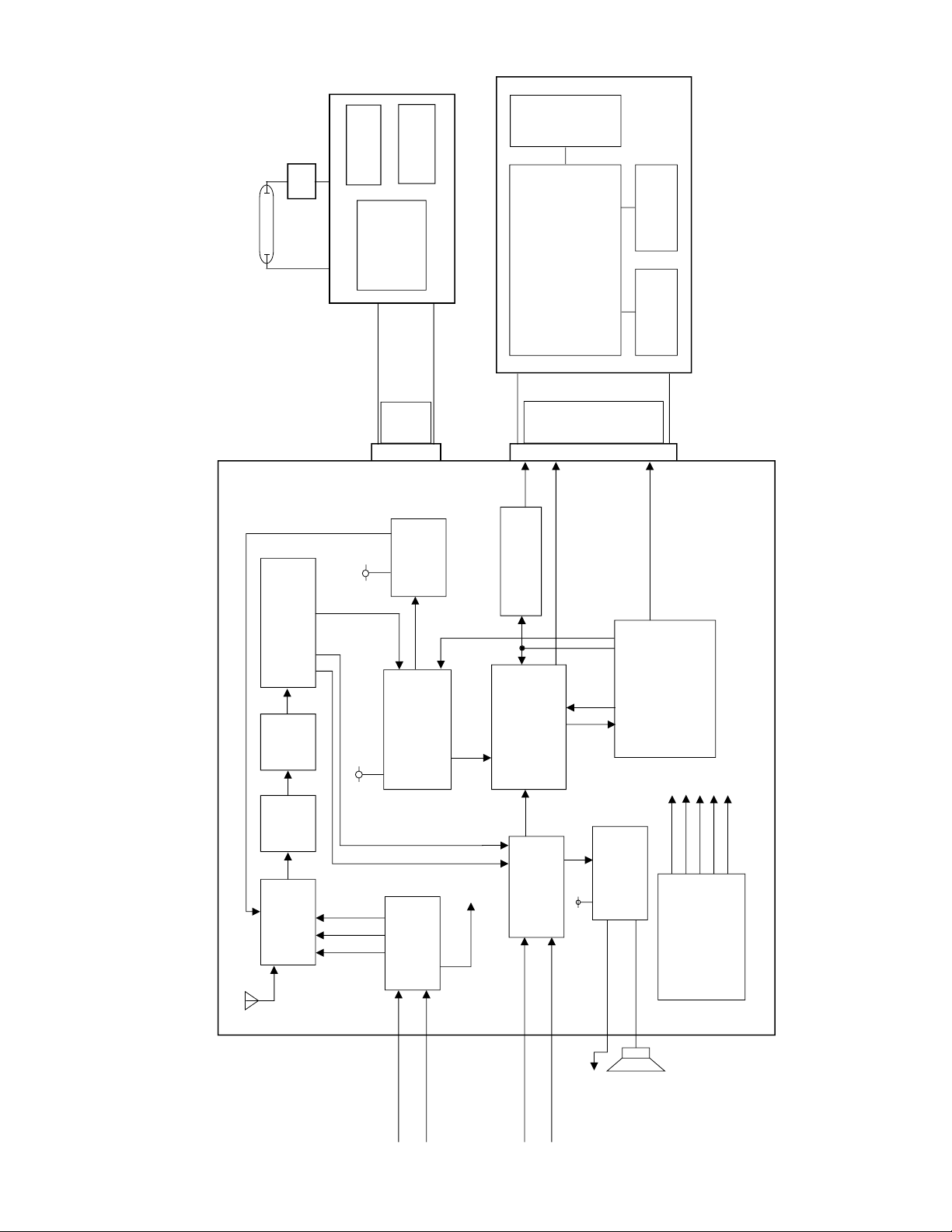
BLOCK DIAGRAM
VCOM AMP
(NJM3414AVP)
L-PCB
BT LAMP
SUB-PCB
VCC2
BS
BV
VCC7
BATTERY 1.5V
x
4 AFT
AC ADAPTOR 6V
VCC1-1 EXT-R
EXT-G
LCM
COD30T3015LN
EXTERNAL VIDEO VIDEO2 VCOM
EXTERNAL AUDIO R,G,B
VCC1-1 AUDIO2
Vcc7(30V)
Vcc6(18.5V)
Vcc5(12V)
Vcc2(4.8V)
Vee1(-10.5V)
CN920
CN700
CSYNC
HDB
FRP
CLR,SRT1,MCLK
BU
VIDEO1
AUDIO1
ANT
TUNER
(TEPE5-01)
LCD
384*243
INVERTER
TRANS
(C-8126)
CH
UPKEY
CH
DOWNKEY
SOURCE
DRIVER SOURCE
DRIVER
GATE DRIVER
EAR
PHONE
SP
VCC2-4
DOWN
UP
VCC1-1
GND
VCC6
VCC5-1
VCC2-5
GND
VEE1
MCLK
CLR
OE
SRTL
SRTR
RESET
GSRT
GPCK
GRES
HCNT
MCLK
CLROESRTL
SRTL
SRTR
RESET
GSRT
GPCK
GRES
HCNT
POWER SW
BAND SW
AV JACK
AUDIO AMP
(NJM2070M)
DC/DC
CONVERTER
TRANS
TFT
CONTROLER
(CM7017L3)
TFT
CHROMA
(IR3Y18A)
TUNING
CONTROLER
(SED3950F)
PRE
AMP SAW
FILTER VIF/SIF
(M51348FP)
TUNING
BT AMP
(BA10358)
BT
— 3 —
CP238
T200
VR730
CP750
CP711
CP324
CP705
CP725
VR710
VR303
CP344
VR300
T300
CP308
VR301 CP106
CP107
CP105
CP108 VR100
CP101
CP109
ADJUSTMENT
Top View Bottom View
1. Vcc2 adjustment, Vcc7, Vcc6, Vcc5, Vee1 voltage check
2. LLD coil adjustment
3. Free running frequency adjustment
4. VOM AC and VCOM DC coarse adjustment
5. Contrast, Bright adjustment
6. COLOR adjustment
7. BCC coil adjustment
8. VCOM DC adjustment
Preparations
1. For the above 1 - 7 adjustments, connect JACK to the ground GND(OV).
Adjustment And Test Point Locations

— 4 —
Adjustment procedures (EV-660C/I/N)
1. VCC2 adjustment, VCC7, VCC6, VCC5, VEE1 voltage check
•Condition
(1) Signal
No signal
(2) Other conditions
Power supply: Vcc1-1 = 5.00 ±0.05 [V]
•Adjustment
Apply 5.00 ±0.05 [V] on Vcc1-1.
Adjust VR100 so that Vcc2 (CP108) voltage becomes 4.80 ±0.02 [V].
•Checking
VCC7 (CP105) = 27.1 ~ 33.4 [V]
VCC6 (CP106) = 18.0 ~ 20.0 [V]
VCC5 (CP107) = 11.0 ~ 13.0 [V]
VEE1 (CP109) = –12.0 ~ –10.0 [V]
•Block diagram
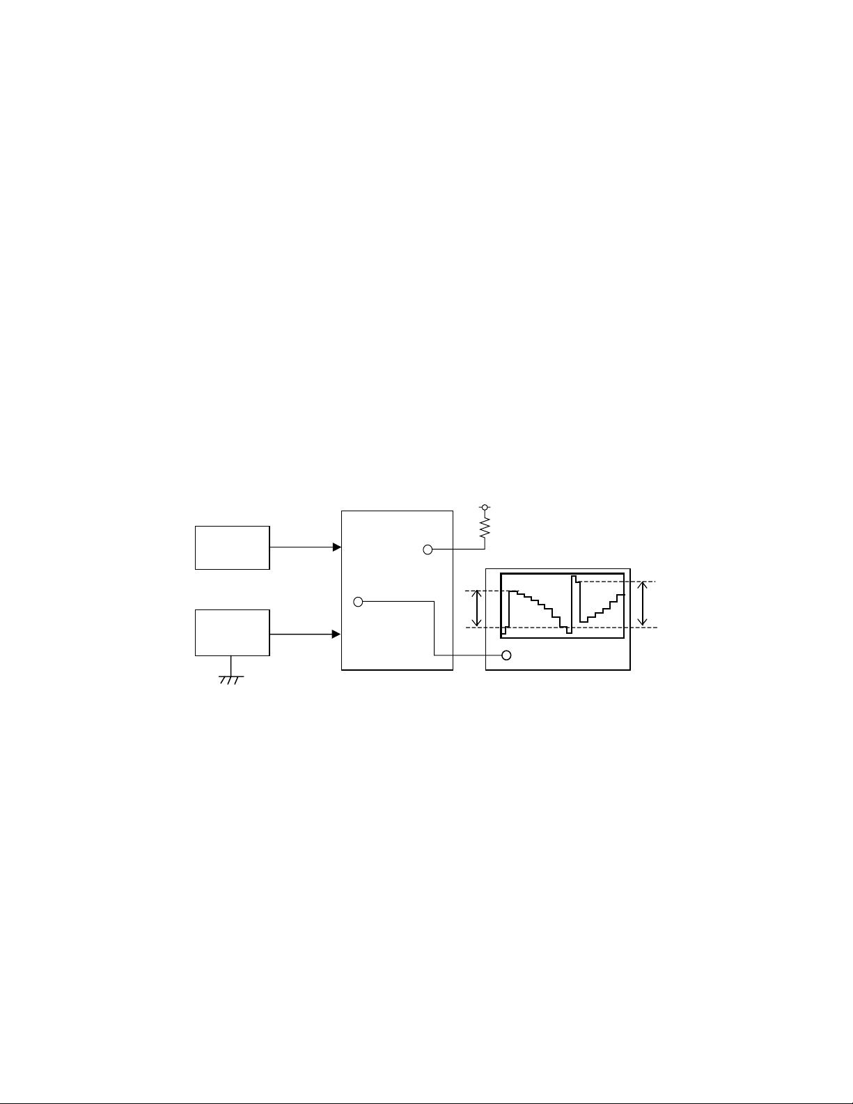
2. LLD coil adjustment
•Conditions
(1) Signals
Broadcasting system: B/G
Color system: PAL color bar
(2) Signal level
Input electric field: 46 ±3 dBµ(IF AGC full gain), P/S = 10 dB
(3) Other conditions
CCIR IF (Input electric field: terminated with 75 Ωresistance)
As to VIDEO signal, use signal source equivalent to TG7.
Power supply: Vcc1-1 = 5.00 ±0.05 [V]
•Adjustment
Monitor video detection signal (CP238) via a low-pass filter of 100 kHz cutoff frequency and adjust LLD coil
T200 so that its DC level is minimum (waveform’s amplitude is maximum).
•Confirmation
There should be no waveform distortion (erroneous synchronization, etc.), under sensitivity (video detector
output level is abnormally small, etc.).
•Block diagram
VDigital
Voltmeter
L-PCB
Stabilizer
VCC1-1
VCC7
VCC6
VCC5
VCC2
VEE1
VCC1-1
IF signal
L-PCB
Adjust to minimize the DC level.
Oscilloscope
DC IN
Detector OUT
Signal
generator
Stabilizer
Low-Pass Filter

— 5 —
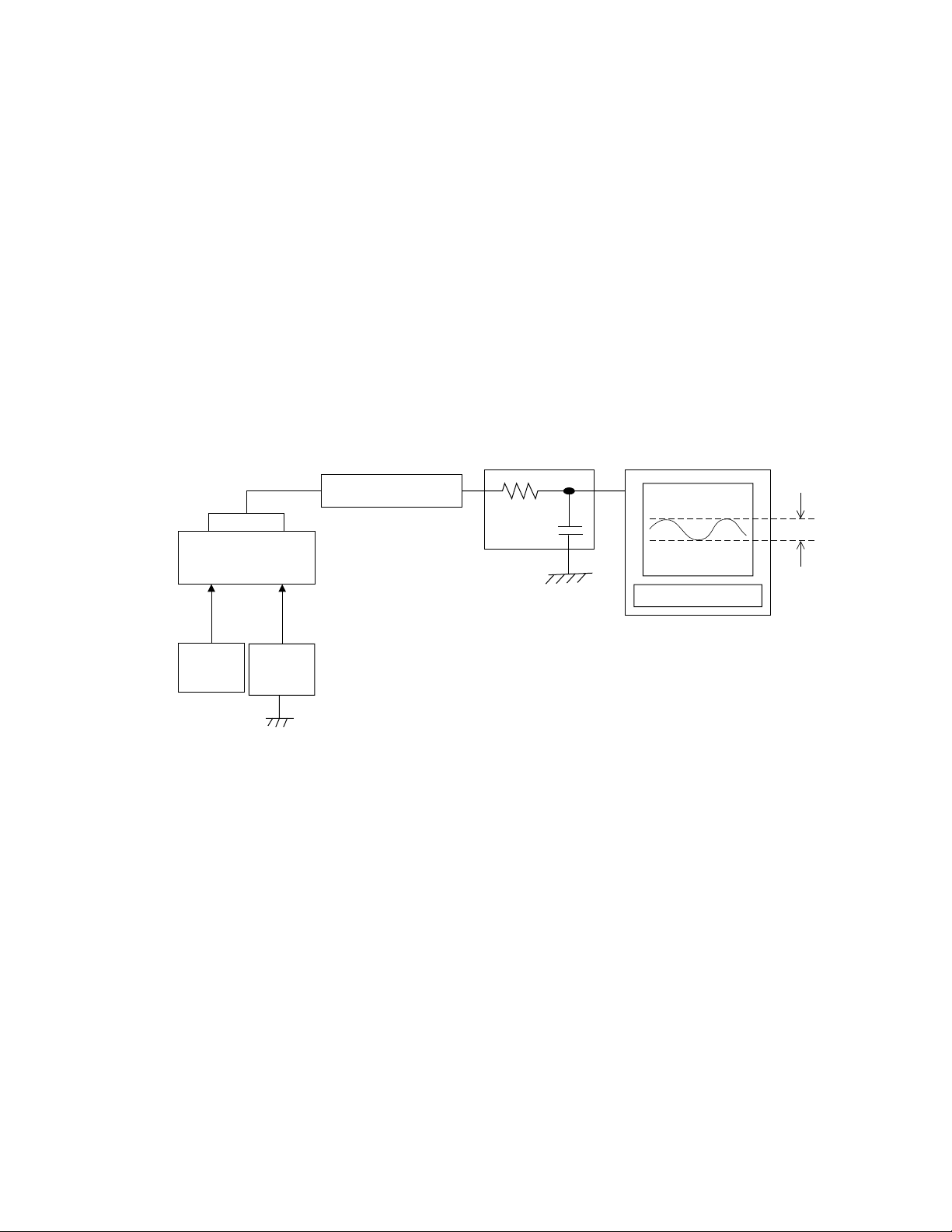
3. Free running frequency adjustment
•Conditions
(1) Signal
No signal (PAL standard signal should be applied only at synchronous check)
(2) Signal level
Input electric field only at synchronous check: 70 ±3 dBµ(terminated with 75Ωresistance),
P/S = 10 dB
(3) Other conditions
CCIR IF input only at synchronous check (input electric field with 75 Ωtermination).
Connect SYF terminal (CP725) and GND.
Power supply: Vcc1-1 = 5.00 ±0.05 [V]
Room temperature: 20 ±10 [°C]
•Adjustment
Monitoring HDB (CP705) with a frequency counter, adjust VR710 so that the frequency is 15.625 ±0.1 [kHz].
•Caution
(1) Disconnect the wire between SYF terminal. Applying IF signal make sure that synchronization is normal
on the display.
•Block diagram
L-PCB
SYF GND
HDB Frequency
Counter
VCC1-1
IF signal
Signal
generator
Stabilizer
4. VCOM AC and VCOM DC coarse adjustment
• Conditions
(1) Signals
Broadcasting system: B/G
Color system: PAL color bar
(2) Signal level
Input electric field: 70 ±3dBµ(terminated with 75Ωresistance), P/S = 10 dB
(3) Others
CCIR IF input (input electric field should be terminated with 75Ωresistance)
Use VIDEO signal equivalent to TG7.
Power supply should be Vcc1-1 = 5.00 ±0.05V.
• Adjustment
(1) Confirm that the amplitude of VCOM output (CP750) is 6.0 ±0.5 [V].
(2) Adjust VR730 so that Low level voltage of VCOM output (CP750) is 2.4 ±0.2 [V].
•Block diagram
GND
2.4 V
6.0 V
VCC1-1
IF signal
Signal
generator
Stabilizer
L-PCB
CP750
Oscilloscope
— 6 —
5.0 – 0.1 V
3.5 – 0.1 V
VCC1-1
IF signal
Signal
generator
Stabilizer
Oscilloscope
L-PCB
B output
CP308
22 KΩ
VCC2-3
5. Contrast, Bright adjustment
• Conditions
(1) Signals
Broadcasting system: B/G
Color system: PAL color bar
(2) Signal level
Input electric field: 70 ±3 dBµ(terminated with 75Ωresistance), P/S = 10 dB
(3) Others
CCIR IF input (input electric field should be terminated with 75Ωresistance)
As to VIDEO signal, use signal source equivalent to TG7.
Supplying power should be VCC1-1 = 5.00 ±0.05 V
•Adjustment
(1) Apply VCC2-3 (CP344) voltage on KILLER terminal (CP308) via 22 kΩresistance.
(2) Triggering FRP signal (CP711), observe VB waveform (CP324) and adjust BRIGHT VR so that pedes-
tal-pedestal voltage becomes 5.0 ±0.1[V].
(3) Adjust VR303 so that VB (CP324) waveform's pedestal - white peak voltage is 3.5 ±0.1[V].
•Caution
(1) Make sure that waveforms are not distorted.
(2) After the adjustment, disconnect VCC2-3 voltage from the killer terminal.
(Reference: Use white 75% for PAL color bar.)
(3) Do not move BRIGHT VR until TINT and COLOR adjustments are completed.
•Block diagram

— 7 —
6. COLOR adjustment
•Condition
(1) Signal
Broadcasting system: B/G
Color system: PAL color bar
(2) Signal level
Input electric field: 70 ±3 dBµ(75Ωtermination), P/S = 10 dB
(3) Other conditions
CCIR IF input (input electric field should be terminated with 75Ωresistance).
Use VIDEO signal equivalent to TG7.
Apply voltage of Vcc1-1 = 5.00 ±0.05 [V]
•Adjustment
Adjust VR300 so that 4th pulse of VB waveform's (CP324) pedestal-peak amplitude is 3.5 Vp-p.
•Caution
(1) Perform after Contrast adjustment.
(2) VB waveform's pedestal-pedestal voltage should be fixed on 5.0 ±0.1 [V].
•Block diagram
VCC1-1
IF signal
Signal
generator
Stabilizer
L-PCB
B output
Oscilloscope
3.5 Vp-p
7. BCC coil adjustment
•Condition
(1) Signal
Broadcasting system: B/G
Color system: PAL color bar
(2) Signal level
Input electric field: 70 ±3 dBµ(75Ωtermination), P/S = 10 dB
(3) Other conditions
CCIR IF input (input electric field should be terminated with 75Ωresistance).
Use VIDEO signal equivalent to TG7.
Apply voltage of Vcc1-1 = 5.00 ±0.05 [V]
•Adjustment
Adjust BCC coil (T300) so that center 2 pulses of VB waveform (CP324) become level (3.5 ±0.1 [V].)
•Caution
(1) Perform after COLOR adjustment.
(2) VB waveform's pedestal-pedestal voltage should be fixed on 5.0 ±0.1 [V].
•Block diagram
VCC1-1
IF signal
Signal
generator
Stabilizer
L-PCB
B output
Oscilloscope
— 8 —
VCC1-1
AV JACK
Signal
generator Stabilizer
EV-660C/I/N
Photo diode
S1133 Photosensor amp.
C2719
B.P.F.
Oscilloscope
8. VCOM DC adjustment
• Conditions
(1) Signals
Broadcasting system: B/G
Color system: PAL
(2) Signal: Provide any PAL signal from AV Jack.
(3) Others
Power supply should be Vcc1-1 = 5.00 ±0.05V.
• Adjustment
Monitoring Photo sensor AMP output with an oscilloscope via 50Hz band-pass filter, adjust VCOM DC VR
(VR730) so that 50Hz ripple component is minimum.
• Caution
Perform this adjustment when you replaced the display module.
Use specified jig to replace photoelectric parts
•Block diagram
This manual suits for next models
3
Table of contents
Other Casio LCD TV manuals

Casio
Casio FV-600BA Troubleshooting guide

Casio
Casio SY-20B User manual

Casio
Casio TV-480 User manual

Casio
Casio TV-480 User manual

Casio
Casio TV-470 B User manual

Casio
Casio EV-680 User manual

Casio
Casio 850TR/900 User manual

Casio
Casio EV-2500B Troubleshooting guide

Casio
Casio JY-70B Troubleshooting guide

Casio
Casio TV-890 User manual


