Caswell CAR-5040 Series User manual

CAR-5040 Series
Communication Appliance
Users Manual
Revision: 1.1

Table of Contents
Chapter 1 Manual Overview ....................................................................................... 3
1.1 About This Manual .......................................................................................................... 3
1.2 Intended Audience .......................................................................................................... 4
1.3 Manual Contents Descriptions .......................................................................................................... 4
1.4 Technical or Customer Support ........................................................................................................ 4
Chapter 2 Introduction ................................................................................................ 5
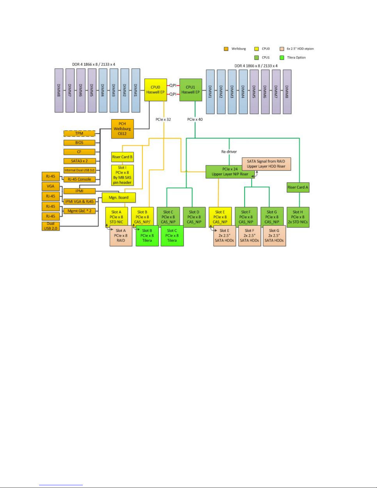
2.1 Processor and chipset Overview ..................................................................................... 5
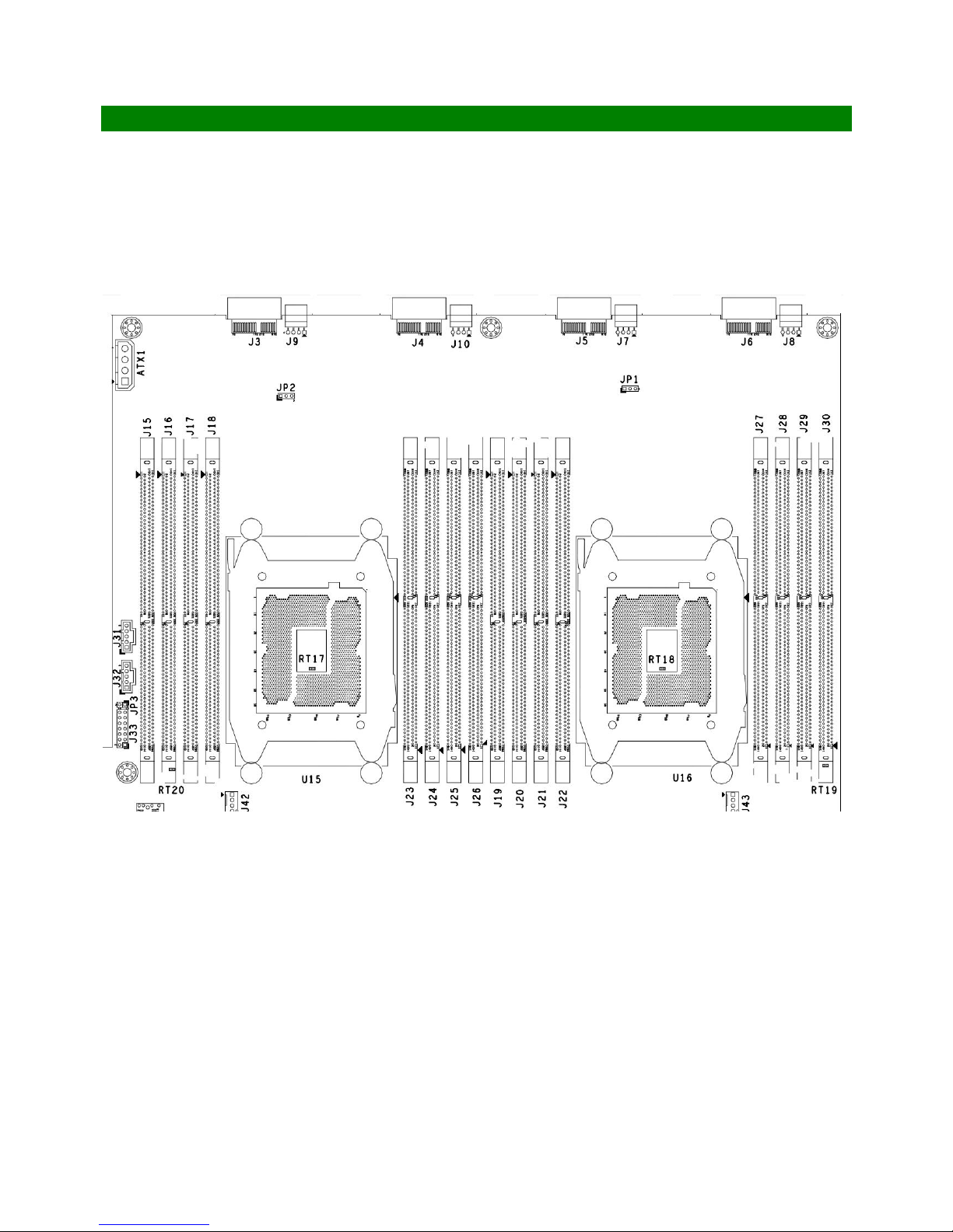
2.2 Serverboard Features...................................................................................................... 6
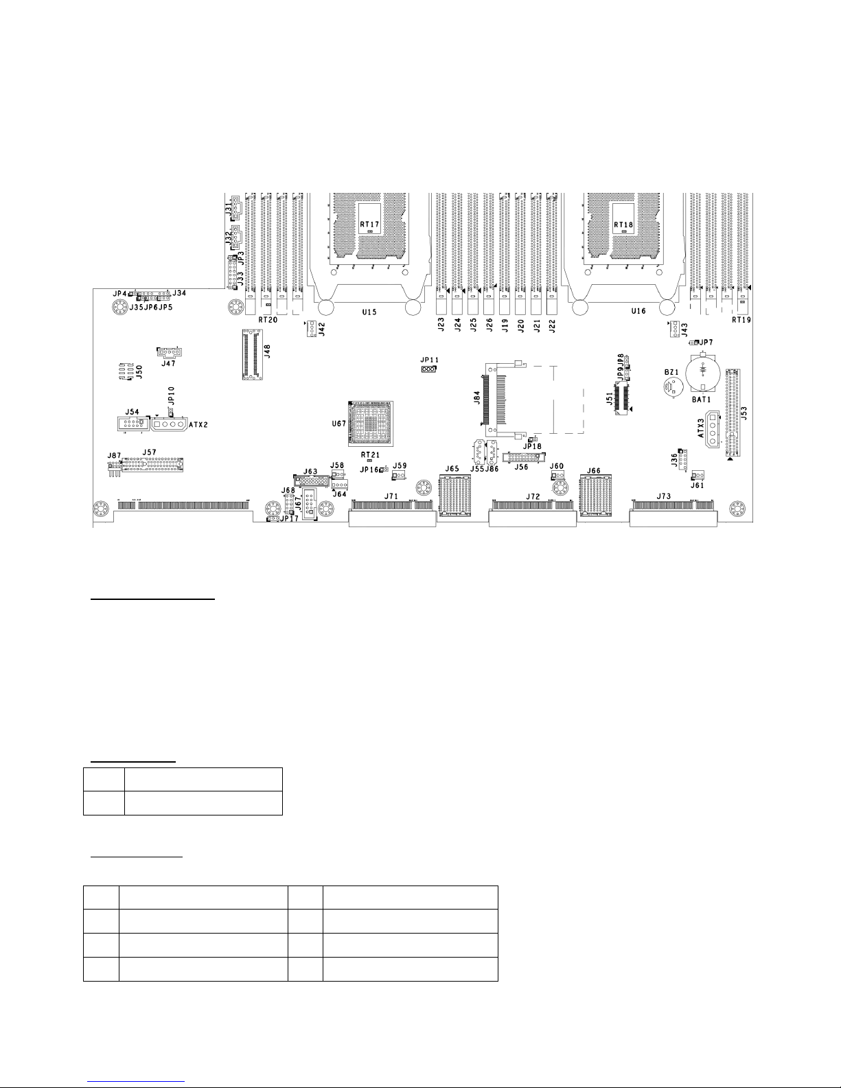
2.3 Jumper Setting ................................................................................................................ 8
Chapter 3 Hardware Installation Procedures .......................................................... 25
3.1 Before You Begin .......................................................................................................... 25
3.2 Install a Different Processor........................................................................................... 26
3.3 Remove and Install DIMM ............................................................................................. 29
3.4 Remove and Install Battery............................................................................................ 31
3.5 Open the Chassis .......................................................................................................... 31
3.6 Remove Front Penal and Bracket .................................................................................. 32
3.7 Remove PSU ................................................................................................................ 33
3.8 Remove HDD tray and slot E/F/G riser .......................................................................... 38
3.9 Remove ABM-5040 ....................................................................................................... 39
3.10 Remove Fan module ..................................................................................................... 40
3.11 Remove Main Board ...................................................................................................... 41
Chapter 4 BIOS Settings ........................................................................................... 42
4.1 lntroduction .................................................................................................................... 42
4.2 Main ..................................................................................................................... 43
4.3 Advanced ..................................................................................................................... 44
4.4 IntelRCSetup ................................................................................................................. 56
4.5 Server Management ...................................................................................................... 75
4.6 Security ..................................................................................................................... 76

4.7 Boot 77
4.8 Save & Exit .................................................................................................................... 78
4.9 BIOS status and Beep codes ......................................................................................... 79
Chapter 5 CAR-5040 IPMI ......................................................................................... 83
5.1 Document control .......................................................................................................... 83
5.2 Revision History ............................................................................................................ 83
5.3 LOM and System Management Overview ..................................................................... 83
5.4 Using LOM WebGUI ...................................................................................................... 84
5.5 System Configuration from WebGUI .............................................................................. 90
5.6 System Monitoring and Maintenance from WebGUI .................................................... 100
5.7 System BMC Management from WebGUI ................................................................... 110
5.8 Utilities ................................................................................................................... 127
5.9 Software Design Specification of Fan Control Algorithm .............................................. 132
Chapter 1 Manual Overview
1.1 About This Manual
This manual contains all required information for setting up and evaluating the CAR-5040. The CAR-5040 is
based on the Intel® C612 chipset and supports single or dual Intel®Xeon® E5 2600v3processors in
FCLGA2011-3 sockets an up to 256 GB of DDR4 2133 registered ECC SDRAM.

1.2 Intended Audience
This manual is intended for use by engineer who are evaluating and developing their own
application on the CAR-5040.
1.3 Manual Contents Descriptions
This manual describes how to configure the CAR-5040 to meet various operating
requirement, which is organized as follows:
Section 1 provides an overview of this manual, information about contacting customer
support, and general instructions about how registers are described.
Section 2 provides an overview of the components in the CAR-5040, a description of the
CAR-5040's features, and a description of the development environment.
Section 3 specifies the system and device requirements.
Section 4 provides a performance demonstration for the CAR-5040 including instructions on
compiling and installing software. The measurement of network performance is also
provided.
Section 5 introduces the PCIe data transmission daemon.
Section 6 provides the appendices.
1.4 Technical or Customer Support
You can reach CASwell customer support in the following ways:
Visit the CASwell web site at
http://www.cas-well.com/
E-mail your questions to
tech.support@cas-well.com

Chapter 2 Introduction
2.1 Processor and chipset Overview
Built upon the functionality and the capability of the Intel ® Xeon® E5-2600 v3 series processors and the C612
chipset, the CAR-5040 provides the performance and feature required for dual processors based workstation
platform.

2.2 Serverboard Features
Item Description
CPU Dual Grantley-EP, socket R3 120W
Memory Up to Sixteen 1.2v DDR4 2133 ECC RDIMM/ LRDIMM/ slots
Ethernet I/O Up to Six proprietary NIC swappable multiple slots and Two low profile
standard NIC.
Bypass Feature Based on CASwell NIP modules
Extension Six PCIe x 8 with Two PCIe x 8 add-on card slots
HDD Two 3.5” HDD tray w/ locks
Up to 6 2.5” Hot Plugging HDDs
LCD panel External 16x2 character or 128x64 graphical LCD
USB External Dual USB 2.0 ports
Console RJ-45 interface
VGA Optional from LOM or VGA module
Power 550W CRPS Structural redundant PSU
Dimension 465(W) x 533.8(D) x 88.5(H)
18.6”(W) x 21.35”(D) x 3.48”(H)

System Block Diagram

2.3 Jumper Setting
CAPB-5040 Jumper Setting
˙Components Map
TOP Layer

(Lower)
Thermal Sensor List
RT17:CPU0 Temperature Sensor
RT18:CPU1 Temperature Sensor
RT19:Memory Temperature Sensor
RT20:Memory Temperature Sensor
RT21:System Temperature Sensor
CPU SOCKET
U15
CPU0
U16
CPU1
DIMM SOCKET
CPU0
J15
CPU 0, CH A DIMM0 J17
CPU 0, CH B DIMM0
J16
CPU 0, CH A DIMM1 J18
CPU 0, CH B DIMM1
J24
CPU 0, CH D DIMM0 J26
CPU 0, CH C DIMM0
J23
CPU 0, CH D DIMM1 J25
CPU 0, CH C DIMM1

CPU1
J19
CPU 1, CH E DIMM0 J21
CPU 1, CH F DIMM0
J20
CPU 1, CH E DIMM1 J22
CPU 1, CH F DIMM1
J28
CPU 1, CH H DIMM0 J30
CPU 1, CH G DIMM0
J27
CPU 1, CH H DIMM1 J29
CPU 1, CH G DIMM1
Jumper & Connector List
Connector Function Remark
JP1 CPU1 IR PWM IC Programming
JP2 CPU0 IR PWM IC Programming
JP3 Auto Power Button ˙1-2:Enable★
˙Open:Disable
JP4 NMI Button ˙Open★
JP5 CPLD TCK ˙1-2:Disable★,
˙2-3:Enable
JP6 CPLD TDO ˙1-2:CPLD Programming★,
˙2-3:LA Trigger
JP7 Case Open
JP10 Watchdog Timer Reset ˙1-2:Enable★
˙Open:Disable
JP11 CMOS Clear Jumper ˙1-2:Clear RTC Register
˙2-3:Normal★
JP16 Flash Descriptor Security Override ˙1-2:Override
˙Open:No Override★
JP17 GPIO Port(J68) Power Selector ˙1-2:5V
˙2-3:3.3V★
JP18 CF Function Selection ˙Open:Enable the output to the ATA bus
★
˙Close:Disable the output to the ATA bus
J3/J4/J5/J6 FAN module Slots
J7/J8/J9/J10 System FAN
J31 PMBus SMBus Connector
J32 PCH SMBus Connector

J33 Front Panel Control
J34 CPLD JTAG Connector
J35 CPLD Hook1 Select Open★
J36 Debug Port
J37 CPLD Debug Mode Open★
J42 CPU0 Fan
J43 CPU1 Fan
J47 IPMI SMBus Connector
J48 Mini-SAS Connector-CPU0
J49 IPMI
J50 Serial port Header
J51 XDP
J53 PCI-E Slot H x8(Standard)-CPU1
J54 VGA
J55 SATA Port 0 (6Gb/s)
J56 TPM
J57 HDD Board Connector
J58
J59
J61
NIP Module Fan
J63 USB3.0
J64 Power Header
J60 Smart Fan
J67 COM Port
J68 GPIO
J82 Manager Board Slot
J84 CF Connector
J86 SATA Port 1 (6Gb/s)
J87 DDR3 SODIMM NCSI Pin Header
BAT1 Battery
BZ1 Buzzer
U67 PCH (C612)
ATX1
ATX2
ATX3
Power Connector
J65
J66
Front Upper Layer NIP Riser(Not support
Tilera NIP module)
J65 Signal from CPU0 (Slot E)
J66 Signal from CPU1 (Slot F/G)

J71 PCI-E Slot B x8 (CASwell NIP)-CPU0 Support Tilera NIP module
J72 PCI-E Slot C x8 (CASwell NIP)-CPU1 Support Tilera NIP module
J73 PCI-E Slot D x8 (CASwell NIP)-CPU1 Support Tilera NIP module
(Default Setting:“★”)
˙Pin Header definition
JP1(CPU1):IR PWM IC Programming
JP2(CPU0):IR PWM IC Programming
Pin No. Signal Description
1 CLOCK
2 DATA
3 GND
J7/J8/J9/J10:System FAN
1 2 3 4
Pin No. Signal Description
1 GND
2 12V
3 SENSE
4 PWM Control
J31:PMBus SMBus Connector
J32:PCH SMBus Connector
1 2 3 4 5
Pin No. Signal Description
1 CLOCK
2 DATA
3 ALERT

4 GND
5 3.3V
J33:Front Panel Control
2 4 6 8 10 12 14
1 3 5 7 9 11 13
Pin No. Signal Description Pin No. Signal Description
1 HDD LED+ 2 PWR LED+
3 HDD LED- 4 PWR LED-
5 OPMA_LOCAL_LOCK_N 6 OPMA_LOCAL_LOCK_N
7 RESET+ 8 PWRON+
9 RST_TO_DEFAULT_BTN_N 10 PWRON-
11 CHASSIS LED+ 12 FAULT LED+
13 CHASSIS LED- 14 FAULT LED-
J34:CPLD JTAG Connector
1 2 3 4 6 7 8
Pin No. Signal Description Pin No. Signal Description
1 3VSB
2 TDO 6 TMS
3 TDI 7 GND
4 GND 8 TCK
J36:Debug Port
Pin No. Signal Description Pin No. Signal Description
1 LPC_LAD0 2 P3V3
3 LPC_LAD1 4 RST_PLTRST_B_N
5 LPC_LAD2 6 LPC_FRAME_N
7 LPC_LAD3 8 CLK_33M

9 NC 10 GND
J42:CPU0 Fan
J43:CPU1 Fan
1 2 3 4
Pin No. Signal Description
1 GND
2 12V
3 NO SENSE Function
4 NC
J47:IPMI SMBus Connector
1 2 3 4 5
Pin No. Signal Description
1 CLOCK
2 DATA
3 3.3V
4 GND
5 3.3V
J50:Serial Port Header
2 4 6 8
1 3 5 7
Pin No. Signal Description Pin No. Signal Description
1 IPMI_DATA 2 GND
3 IPMI_CLOCK 4 GND
5 IPMI_485D- 6 GND
7 IPMI_485D+ 8 GND

J54:VGA
2 4 6 8 10
1 3 5 7 9
Pin No. Signal Description Pin No. Signal Description
1 RED 2 DDC_CLOCK
3 GREEN 4 GND
5 BLUE 6 DDC_DATA
7 V-SYNC 8 GND
9 H-SYNC 10 NC
J56:TPM
2 4 6 8 10 12 14 16 18 20
1 3 5 7 9 11 13 15 17 19
Pin No. Signal Description Pin No. Signal Description
1 TPM_CLK 2 GND
3 LFRAME# 4 NC
5 TPM_RESET# 6 5V
7 LAD3 8 LAD2
9 VCC3 10 LAD1
11 LAD0 12 GND
13 SMB_CLK 14 SMB_DATA
15 3VSB 16 SERIRQ
17 GND 18 GND
19 3VSB 20 LDRQ#1
J58/J59/J61:NIP Module Fan
1 2 3
Pin No. Signal Description

1 GND
2 12V
3 NC
J60:Smart Fan
1 2 3
Pin No. Signal Description
1 GND
2 PWM Control
3 Sense
J63:USB3.0
1 2 3 4 5 6 7 8 9 10
20 19 18 17 16 15 14 13 12 11
Pin No. Signal Description Pin No. Signal Description
20 KEY 1 +5V
19 +5V 2 SSRX2_N
18 SSRX1_N 3 SSRX2_P
17 SSRX1_P 4 GND
16 GND 5 SSTX2_N
15 SSTX1_N 6 SSTX2_P
14 SSTX1_P 7 GND
13 GND 8 D1_N
12 D2_N 9 D1_P
11 D2_P 10 GND
J64
1 2 3 4
Pin No. Signal Description
1 12V
2 GND
3 GND
4 5V

J67:COM Port
2 4 6 8 10
1 3 5 7 9
Pin No. Signal Description Pin No. Signal Description
1 DCD 2 DSR
3 RXD 4 RTS
5 TXD 6 CTS
7 DTR 8 RI
9 GND 10 NC
J68:GPIO
2 4 6 8 10
1 3 5 7 9
Pin No. Signal Description Pin No. Signal Description
1 GP67 2 GP60
3 GP66 4 GP61
5 GP65 6 GP62
7 GP64 8 GP63
9 GND 10 5V/3.3V
J87:DDR3 SODIMM NCSI Pin Header
Pin No.
Signal Description Pin No.
Signal Description
1 NCSI_Tx0 2 NCSI_CLK
3 NCSI_Tx1 4 NCSI_CRS_DV
5 NCSI_Rx0 6 NCSI_TX_EN

ATX1/ATX2/ATX3:Power Connector
1 2 3 4
Pin No. Signal Description
1 12V
2 GND
3 GND
4 5V

ABM-5040-0 Jumper Setting
˙Components Map
TOP Layer
BOT Layer

˙Jumper & Connector List
Connector Function Remark
J1 Standard PCIe x8 Slot
J2 USB 2.0 Connector
J3 USB 2.0 Connector
J4 Management Port 01 RJ45
J5 Management Port 02 RJ45
J6 IPMI connector ( RJ45 Interface )
J7 Consol port ( RJ45 Interface )
J8 Non Standard Spec PCIe x16 Golden Finger
J87 NCSI Pin Header
U3 LAN 01 Controller IC ( I210AT )
U4 LAN 02 Controller IC ( I210AT )
U5 LAN 02 Controller NVM Flash
U6 LAN 01 Controller NVM Flash
D1 Customized LED Green / Red
D2 Customized LED Green / Red
D3 Customized LED Green / Red
D4 Customized LED Green / Red
SW1 Power Button
SW2 Reset Button / Reset to default ˙TOP-Reset Button
˙BOT-Reset to default
(Default Setting:“★”)
˙Pin Header definition
J87:NCSI Pin Header
Pin
Signal Name Pin
Signal Name
Table of contents
Popular Firewall manuals by other brands

NETGEAR
NETGEAR SRXN3205 - ProSafe Wireless-N VPN Firewall Wireless... installation guide

NETGEAR
NETGEAR FVG318 - ProSafe 802.11g Wireless VPN Firewall 8... Reference manual

Sophos
Sophos XG 105w quick start guide

Draytek
Draytek Vigor2860 Series user guide

Recon
Recon Sentinel quick start guide

Hirschmann
Hirschmann EAGLE 20 Series Reference manual