Chrontel CH7034B Supplement

AN-B013
Application Notes
206-1000-013 Rev1.4, 06/30/2020 1
Chrontel
PCB Layout and Design Guide for CH7034B HDTV/VGA/LVDS Encoder
1.0 INTRODUCTION
Chrontel CH7034B is specifically designed for a portable system that requires connections to LCD display, High
Definition Television (HDTV) or RGB (VGA) monitor. With its advanced video encoder, flexible scaling engine and
easy-to- configure audio interface, the CH7034B satisfies manufactures’ product display requirements and reduces their
cost of development and time-to-market.
This application note focuses only on the basic PCB layout and design guidelines for CH7034B HDTV/VGA/LVDS
encoder. Guidelines in component placement, power supply decoupling, grounding, input /output signal interface are
discussed in this document.
The discussion and figures that follow reflect and describe connections based on the 88-pin QFN package of the
CH7034B. Please refer to the CH7034B datasheet for the details of the pin assignments.
2.0 COMPONENT PLACEMENT AND DESIGN CONSIDERATIONS
Components associated with the CH7034B should be placed as close as possible to the respective pins. The following
discussion will describe guidelines on how to connect critical pins, as well as describe the guidelines for the placement
and layout of components associated with these pins.
2.1 Power Supply Decoupling
The optimum power supply decoupling is accomplished by placing a 0.1μF ceramic capacitor to each of the power
supply pins as shown in Figure 1. These capacitors (C1, C2, C4, C5, C7, C8, C10, C11, C13, C14, C16, C18, C19, C22)
should be connected as close as possible to their respective power and ground pins using short and wide traces to
minimize lead inductance. Whenever possible, a physical connecting trace should connect the ground pins of the
decoupling capacitors to the CH7034B ground pins, in addition to ground vias.
2.1.1 Ground Pins
The analog and digital grounds of the CH7034B should be connected to a common ground plane to provide a low
impedance return path for the supply currents. Whenever possible, each of the CH7034B ground pins should be
connected to its respective decoupling capacitor ground lead directly, then connected to the ground plane through a
ground via. Short and wide traces should be used to minimize the lead inductance. Refer to Table 1 for the Ground pins
assignment.
2.1.2 Power Supply Pins
The power supply include AVDD, AVDD_DAC, VDDH, AVDD_PLL, VDDIO, DVDD, VDDMQ, VDDMS.
Refer toTable1 for the Power supply pins assignment. Refer to Figure 1 for Power Supply Decoupling.
CHRONTEL AN-B013
2 206-1000-013 Rev1.4, 06/30/2020
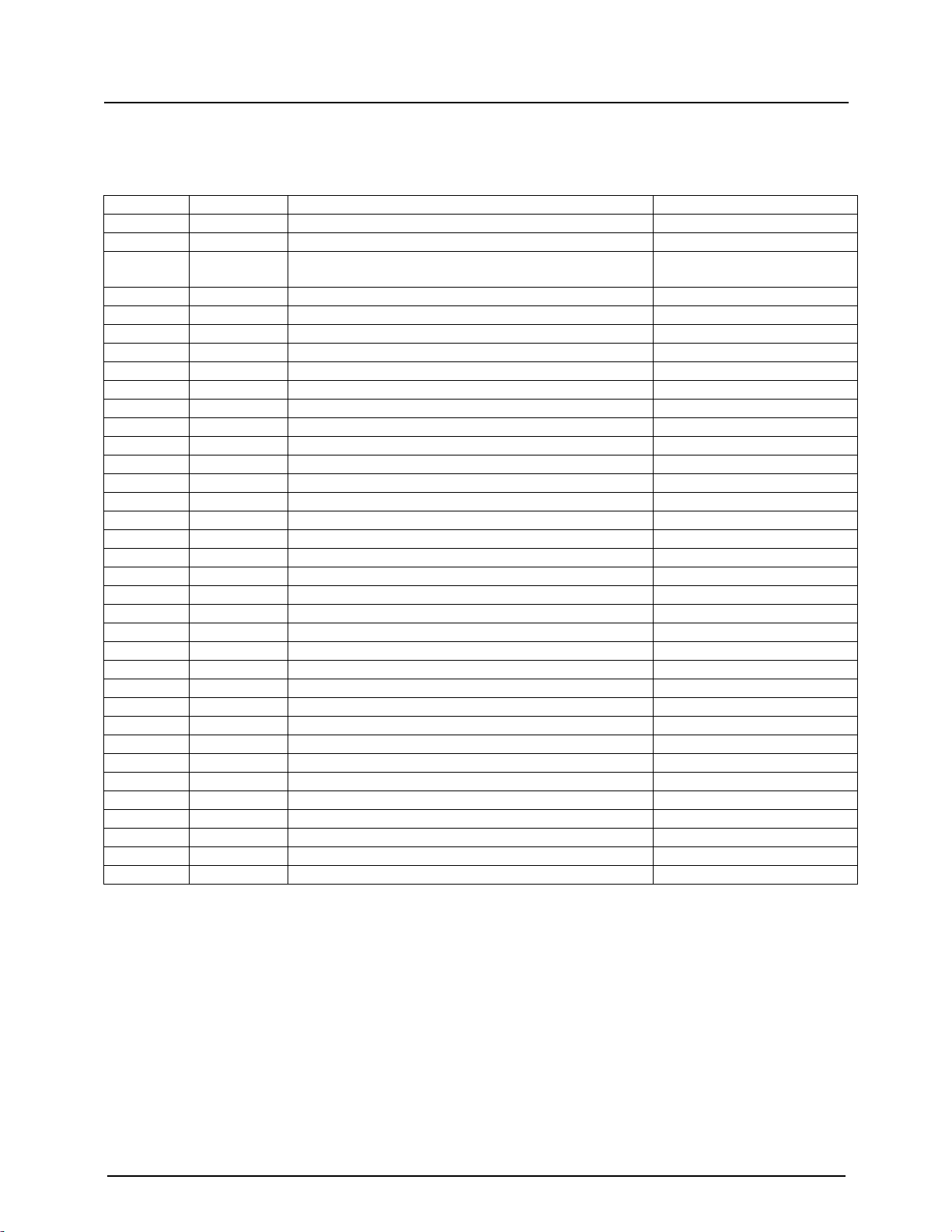
Table 1: Power Supply Pins Assignment of the CH7034B (QFN)
Pin Assignment
#Of Pins
Type
Symbol
Description
30,41
2
Power
VDDH
LVDS Power Supply (3.3V)
10,42
2
Power
DVDD
Digital Power Supply (1.8V)
23,46
2
Power
AVDD
Analog Power Supply (3.3V)
73, 77
2
Power
AVDD_DAC
DAC Power Supply (3.3V)
71
1
Power
AVDD_PLL
PLL Power Supply (1.8V)
53,61
2
Power
VDDMQ
SDRAM output buffer power supply (3.3V)
9,60
2
Power
VDDMS
SDRAM device power supply (3.3V)
33,38
2
Ground
VSSH
LVDS ground
83
1
Power
VDDIO
IO power supply (1.8-3.3V)
45
1
Ground
DGND
Digital ground
22,47
2
Ground
AGND
Analog ground
75, 79
2
Ground
AGND_DAC
DAC ground
70
1
Ground
AGND_PLL
PLL ground
52,62
2
Ground
GNDMQ
SDRAM output buffer ground
59,11
2
Ground
GNDMS
SDRAM ground
1 2
L8 47R100MHz
1 2
L1 47R100MHz
AVDD_PLL
C10
0.1uF C11
0.1uF
AVDD
C12
10uF
1 2
L2 47R100MHz
1 2
L3 47R100MHz
1 2
L4 47R100MHz
C16
0.1uF
C6
10uF
VDDMS
C18
10uF
VDDIOVDDIO
DVDD
C9
0.1uF
C8
0.1uF
VCC3_3
C7
10uF
C21
0.1uF
C22
10uF
C15
0.1uF
C13
10uF
C5
0.1uF
C17
0.1uF
QFN
VDDIO
83
DVDD 10,42
VDDMQ
53,61
VDDMS 9,60
AVDD 23,46
AVDD_PLL 71
VDDH
30,41
DGND 45
GNDMQ
52,62
GNDMS 11,59
AGND 22,47
AGND_PLL 70
VSSH
33,38
AGND
22,47
AVDD_DAC
73,77
AGND_DAC
75,79
U1
CH7034
C4
0.1uF
VCC1_8
C3
0.1uF
C2
0.1uF
C1
10uF
VCC3_3
AVDD_DAC
VDDMQ
VDDHVDDHVDDHVDDHVDDHVDDHVDDHVDDH
C14
0.1uF
C20
0.1uF
C19
10uF
1 2
L5 47R100MHz
1 2
L6 47R100MHz
1 2
L7 47R100MHz
Figure 1: Power Supply Decoupling and Distribution
Note: All the Ferrite Beads described in this document are recommended to have an impedance of less than 0.05 Ω
23 Ωat 25MHz & 47 Ωat 100MHz. Please refer to Fair Rite part #2743019447 for details or an equivalent part can be
used for the diagram.
2.1.3 On chip power-on reset function’s sequence
Power-on reset sequence shown in the Figure 2, should be refer to for design target of generating the ResetB signal
to CH7034B by onboard RC delay. Otherwise, the Power-on Reset Function maybe not work, and the Registers can
NOT be reset to the default values. For hard ware circuit, please refer to 2.3 RESETB.
CHRONTEL AN-B013
206-1000-013 Rev1.4, 06/30/2020 3
Figure 2: Power-on Reset Function’s Sequence on board
ResetB signal is generate by system global reset. In this case, the power supply should be valid and stable for at least
20ms before the reset signal is valid. The pulse width of valid reset signal should be at least 100us. Otherwise, the
chip can’t work well. The timing is shown in Figure 3.
Figure 3: Power-on Reset Function’s Sequence on board
2.2 Internal Reference Pins
• ISET pin
<9ms
AVDD
Other
Powers
ResetB
>20ms
AVDD
Other
Powers
ResetB
>100
us
CHRONTEL AN-B013
4 206-1000-013 Rev1.4, 06/30/2020
This pin sets the DAC current. A 1.2K ohm, 1% tolerance resistor should be connected between this pin and
AGND_DAC as shown in Figure 4. This resistor should be placed with short and wide traces as near as possible to
CH7034B.
R16
1.2K(1%)
ISET 80
AGND_DAC 79
U1
CH7034
QFN
Figure 4: ISET pin connection
2.3 General Control Pins
• RESETB
This pin is the chip reset pin for CH7034B QFN. RESETB pin, which is internally pulled-up, places the device in
the power on reset condition when this pin is low. A power reset switch can be placed on the RESETB pin on the
PCB as a hardware reset for CH7034B QFN or connect to the system’s global reset as shown in Figure 5. When the
pin is high, the reset function can also be controlled through the serial port.
Global reset
U1
RESETB 7
AVDD
SW1
P8058SS-ND
ResetB
C1
0.1uF
R1
1M
U2
RESETB 7Global ResetResetB
AVDD
C2
0.1uF
R2
1M
On board reset
Figure 5: RESETB pin connection
• XI/FIN and XO
CH7034B has capability to accept external crystal with frequencies from 2.3 MHz to 64 MHz.
CHRONTEL AN-B013
206-1000-013 Rev1.4, 06/30/2020 5
QFN
U3
CH7034 XI/FIN 68
XO 67
X1
535-9118-1-ND (27 MHz)
GND
4
P1
1GND 2
P2 3
XI/FIN
XO
C2
18pF
12
C1
18pF
12
Figure 6: Crystal Pins
Reference Crystal Oscillator
CH7034B includes an oscillator circuit that allows a predefined-frequency crystal to be connected directly.
Alternatively, an externally generated clock source may be supplied to CH7034B. If an external clock source is used,
it should have CMOS level specifications. The clock should be connected to the XI pin, and the XO pin should be
left open. The external source must exhibit ±20ppm or better frequency accuracy, and have low jitter characteristics.
If a crystal is used, the designer should ensure that the following conditions are met:
The crystal is specified to be predefined-frequency, ±20 ppm fundamental type and in parallel resonance (NOT
series resonance). The crystal should also have a load capacitance equal to its specified value (CL).
External load capacitors have their ground connection very close to CH7034B (Cext).
To be able to tune, a variable capacitor may be connected from XI to ground.
Note that the XI and XO pins each has approximately 10 PF (Cint) of shunt capacitance internal to the device. To
calculate the proper external load capacitance to be added to the XI and XO pins, the following calculation should
be used:
Cext = (2 x CL) - Cint - 2CS
Where
Cext = external load capacitance required on XI and XO pins.
CL= crystal load capacitance specified by crystal manufacturer.
Cint = capacitance internal to CH7034B (approximately 10-15 pF on each of XI and XO pins).
CS= stray capacitance of the circuit (i.e. routing capacitance on the PCB, associated capacitance of crystal holder
from pin to pin etc.).
In general,
CintXI = CintXO = Cint
CextXI = CextXO = Cext
Such that
CL= (Cint + Cext) / 2 + CSand Cext = 2 (CL- CS) - Cint=2CL- (2CS+ Cint)
Therefore CLmust be specified greater than Cint /2 + CSin order to select Cext properly.
CHRONTEL AN-B013
6 206-1000-013 Rev1.4, 06/30/2020
After CL(crystal load capacitance) is properly selected, care should be taken to make sure the crystal is not
operating in an excessive drive level specified by the crystal manufacturer. Otherwise, the crystal will age quickly
and that in turn will affect the operating frequency of the crystal.
For detail considerations of crystal oscillator design, please refer to AN-06.
2.4 Serial Port Control for CH7034B
• SPC and SPD
SPD and SPC function as a serial interface where SPD is bi-directional data and SPC is an input only serial clock. In
the reference design, SPD and SPC pins are pulled up to +1.8V ~ +3.3V with 6.8 kΩresistors as shown in Figure 7.
• SPCM and SPDM
SPCM and SPDM can automatically load firmware from external EEPROM . In the reference design, SPDM and
SPCM pins are pulled up to +3.0V ~ +3.5Vwith 6.8 KΩresistors as shown in Figure 7.
Note: CH9904 hard wire address should be 57h.
• DDC_SC and DDC_SD
DDC_SC and DDC_SD are used to interface with the DDC of VGA. This DDC pair needs to be pulled up to 5V
through resistors (Refer to Figure 7).
R5
6.8K R7
6.8K
R6
6.8K
SPDM
R9 10K
R8
6.8K
1 2
SPCM
U2
CH9904
GP1
1
GP2
2
GP3
3
GND
4SPD 5
SPC 6
WE 7
VCC 8
R9
6.8K
1 2
VCC3_3VCC3_3
C1
0.1uF
12
VCC3_3
U1
CH7034
SPDM
69 SPCM
72
SPD
55 SPC
54
DDC_SD
64 DDC_SC
63
SPD
R1
6.8K
12
SPC
R2
6.8K
1 2
VCC3_3
QFN
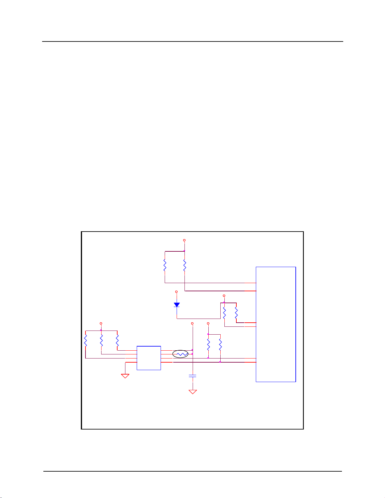
DDC_SC and DDC_SD connect to VGA connector.
The resistor(R3and R4) value according to the capactive Loading.
It is highly recommended to add diode(SM5817) to prevent back
driver from TV or Monitor in VDD5
SPCM and SPDM for autoload
D14
SM5817
VDD5
R4
1.8K
1 2
R3
1.8K
1 2
VDD5_d
Figure 7: Serial Port Interface: SPCM, SPDM and SPC, SPD pins of CH7034B
2.5 Input Pins

CHRONTEL AN-B013
206-1000-013 Rev1.4, 06/30/2020 7
Data Inputs
CH7034B can accept up to 24 data inputs, as shown in Figure 8, from a digital video port of a graphics controller.
The swing is defined by VDDIO (1.2 ~ 3.3V).
Unused Data input pins should be pulled low with 10kΩresistors or shorted to Ground directly.
H/V Sync Pins
The horizontal/vertical sync pins can be used as inputs as shown in Figure 8.
DE/CSB
The DE/CSB pin is used as a data input indicator (Refer to Figure 8). When the pin is high, the input data is active.
When the pin is low, the input data is blanking.
If DE/CSB is not used, it can be left open or pulled down to the Ground.
GCLK
The GCLK input is the clock signal input to the device for using with the H, V, DE and D [23:0] data.
QFN
D[0]
29
D[1]
28
D[2]
27
D[3]
26
D[4]
25
D[5]
21
D[6]
20
D[7]
19
D[8]
18
D[9]
17
D[10]
16
D[11]
15
D[12]
14
D[13]
13
D[14]
12
D[15]
8
D[16]
6
D[17]
5
D[18]
4
D[19]
3
D[20]
2
D[21]
1
D[22]
88
D[23]
87
V
85 H/WEB
86
GCLK
82
DE/CSB
84
Controller
Graphics
Figure 8: CH7034B Data Input Pins
2.6 Miscellaneous Pins
•IRQ
This pin should be connected with graphic controller directly.
2.7 Video Output

CHRONTEL AN-B013
8 206-1000-013 Rev1.4, 06/30/2020
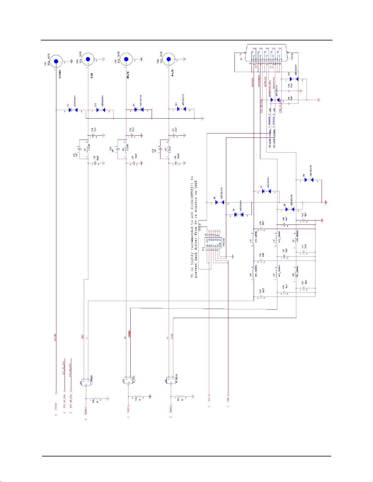
YPbPr and RGB+ Csync output
CH7034B supports both RGB+Csync and HDTV YPbPr output format. The resolution is from 480P to 720P and
1080i and 1080P. In RGB+Csync output format, the Csync high level is the same with AVDD power supply. Csync
pin is a COMS push-pull output pin, customer can use other circuit to change is high level to 0.7V or other voltage
level according to different Receivers. ( Refer to Figure 9)
VGA output
VGA standard output signal level of Hsync and Vsync is more than 2.4V. CH7034B Hsync and Vsync output signal
level is same with AVDD power supply. Customer can use 74ACT08 (AND GATE) to pull high this signal level to
5V(recommend to add the diode).. It is recommended but not necessary. ( Refer to Figure 9)

CHRONTEL AN-B013
206-1000-013 Rev1.4, 06/30/2020 9
R39 75
12
C46
10pF
12
MONHSYNC
MONRED
C48
22pF
12
C49
10pF
12
JP6
Y_GREEN
12
3
C51
10pF
12
L20
47R 100MHz
12
JP7
Pr_RED
12
3
JP8
Pb_BLUE
12
3
C52
22pF
12
L21
47R 100MHz
12
C53
10pF
12
MONVSYNC
CSYNC1
R40 75
12
It is h i ghly r ecommen d to add the dio de in power
supply of 74ACT08, it can prevent the back drive
from TV or Monitor
U5A 74ACT08
A1
B2
Y
3
DAC01
U5B 74ACT08
A4
B5
Y
6
DAC11
DAC21
VSO1
HSO1
Pr
BLUE
RED
Y
Pb
GREEN
MONGREEN
MONBLUE
L17
47R 100MHz
1
2
L18
47R 100MHz
1
2
C47
22pF C50
22pF
L19
150-220R100MHz
1
2
L16
150-220R100MHz
1
2
C43
10pF
12
C44
22pF
12
CSYNC CN1
RCA JACK
1
2
L12
0.33uH
12
C37 1pF
12
C39
27pF
12
C38 100pF
12
C40 1pF
12
L13
0.33uH
12
C41 100pF
12
C42
27pF
12
CN3
RCA JACK
1
2
CN4
RCA JACK
1
2
C34 1pF
12
R38 75
12
C36 100pF
12
L11
0.33uH
12
CN2
RCA JACK
1
2
C35
27pF
12
Y/R
Pr/B
Pb/G
D1
AZ5125-01H
12
C45
10pF
12
P1
VGA
11
22
33
44
55
66
77
88
99
10 10
11 11
12 12
13 13
14 14
15 15
16
16 17 17
L15
47R 100MHz
1
2
L14
47R 100MHz
1
2
CSYNC
D2
AZ5125-01H
12
D3
AZ5125-01H
12
D4
AZ5125-01H
12
D5
AZ5125-01H
12
D6
AZ5125-01H
12
D7
AZ5125-01H
12
D8
AZ5125-01H
12
D9
AZ5125-01H
12
MONSCL
D10
AZ5125-01H
12
MONSDA
D11
AZ5125-01H
12
Figure 9: CH7034B YpbPr, RGB+Csync and VGAoutput
Note: In order to minimize the hazard of ESD, a set of protection diodes (AZ5125-01H) are highly recommendedfor
each DAC and Sync Output.
CHRONTEL AN-B013
10 206-1000-013 Rev1.4, 06/30/2020
2.8 LVDS Output
The LVDS output signals are LDCx* and LDCx. The LVDS is a differential interface with a nominal swing 200mV.
The following rules applies to the signals:
1. Keep traces as short as possible.
2. Make these traces have 100 ohm differential impedance.
3. Trace widths should be 5 mils.
4. Intra Pair spacing (spacing between the “+” and “-” pairs) should be 7mils.
5. Inter Pair spacing (spacing between one differential pair and another) should be a minimum of 20 mils.
6. Difference in trace lengths between “+” and “-” pairs should be within 5mils.
7. Difference in trace lengths among Inter pairs should be within 10mils.
8. “+” and “-” pairs should be routed in parallel.
2.9 Important Design Considerations
• LVDS Power
Close attention must be paid to the power supplied to the LVDS backlight and the LVDS panel. Power requirements
may differ from panel to panel. Please check the panels’ power and backlight voltage specifications.
ENABLK(pin58) and ENAVDD(pin57) of the CH7034B can be used as control signal to turn on the power to the
LVDS backlight and the LVDS logic circuitry.
• PWM
PWM can be used to control the backlight luminance level. The duty cycle of pwm wave can varies between 0 and 1
with a step of 1/255 and the frequency of PWM wave can be 100Hz, 200Hz, 2KHz, 4KHz, 16KHz, 32KHz, 64KHz,
and 128KHz via register setting.
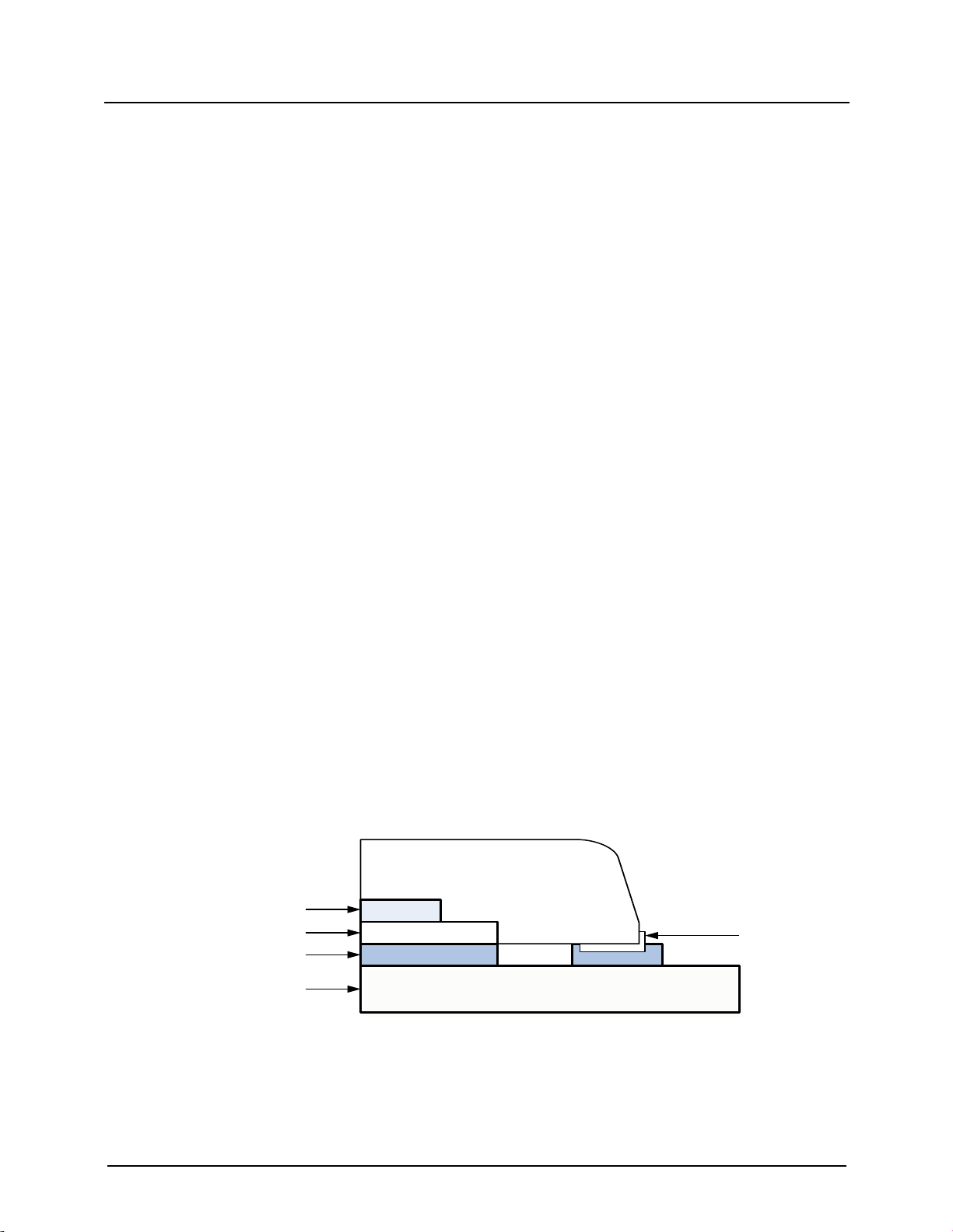
2.10 Thermal Exposed Pad Package
The CH7034B is available in 88-pin QFN package with thermal exposed pad package. The advantage of the thermal
exposed pad package is that the heat can be dissipated through the ground layer of the PCB more efficiently. When
properly implemented, the exposed pad package provides a means of reducing the thermal resistance of the
CH7034B.
Careful attention to the design of the PCB layout is required for good thermal performance. For maximum heat
dissipation, the exposed pad of the package should be soldered to the PCB as shown in Figure 10.
Die
Exposed Pad
Solder
PCB
Pin
Figure 10: Cross-section of exposed pad package
Thermal pad dimension is from 6.6mm to 6.9mm (min to max), 6.6mm x 6.6mm is the minimum size recommended
for the thermal pad, and 6.9mm x 6.9mm is the maximum size. The thermal land pattern should have a 5x5 grid
array of 1.0 mm pitch thermal vias connected to the ground layer of the PCB. These vias should be 0.3mm in
diameter with 1 oz copper via barrel plating. Please refer to Figure 11.
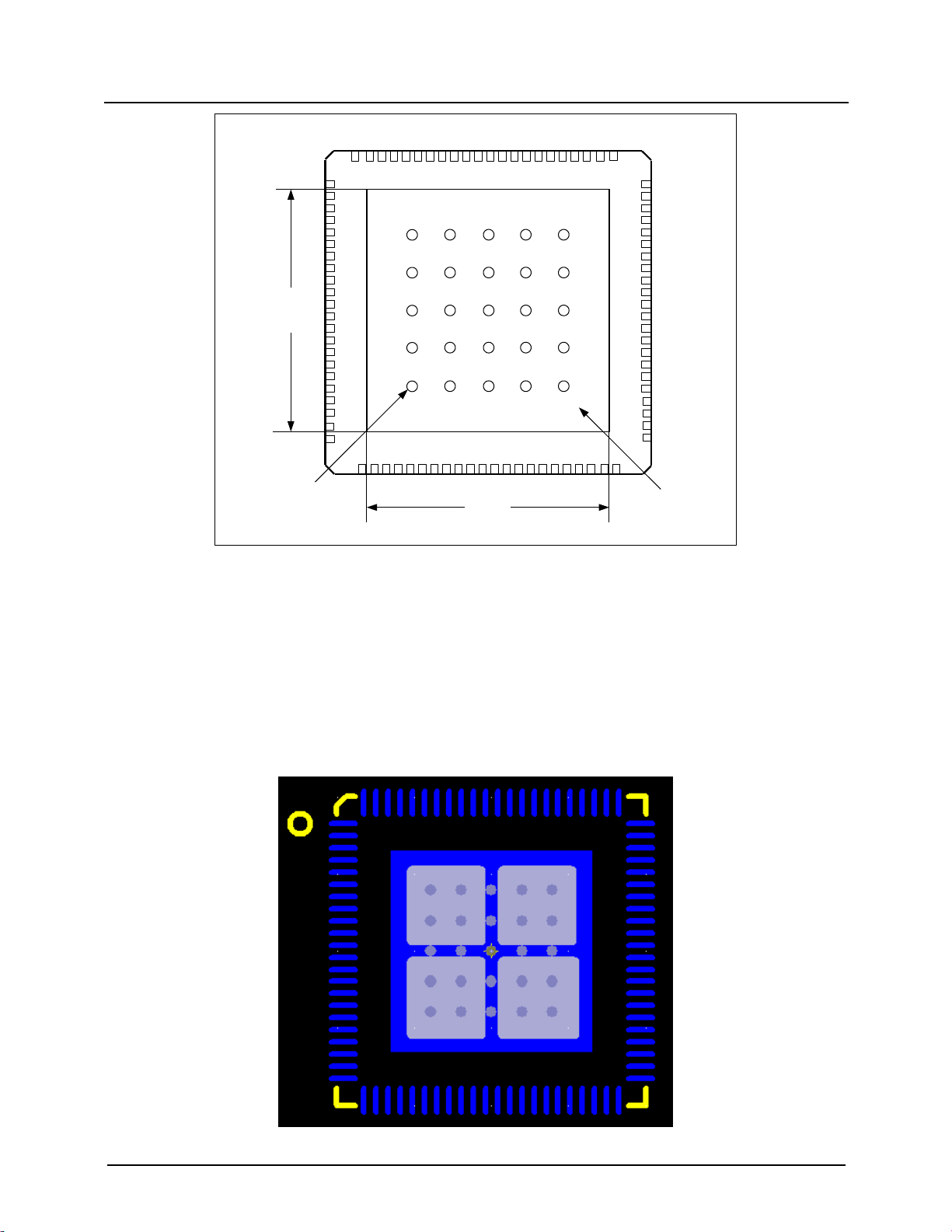
CHRONTEL AN-B013
206-1000-013 Rev1.4, 06/30/2020 11
6.6 mm
6.6 mm Exposed Pad
land pattern
Thermal Via Array
(5x5) 1 mm Pitch
0.3 mm diameter
Figure 11: Thermal Land Pattern
When applying solder paste to the thermal land pattern, the recommended stencil thickness is from 5 to 8 mils.
Thermal resistance was calculated using the thermal simulation program called ANSYS.
2.11 QFN Package Assembly
For the assembly process, it is important to limit the amount of solder paste that is put under the thermal pad. If too
much paste is put on the PCB, the package may float during assembly. Compared with the solder mask of thermal
pad, the paste mask should be shrank to70%~80%. Figure 12 shows a paste mask pattern in gray for the thermal
pad.
Figure12: Thermal Pad Paste Mask Pattern

CHRONTEL AN-B013
12 206-1000-013 Rev1.4, 06/30/2020
3.0 REFERENCE DESIGN EXAMPLE
The figures below are the reference schematic of CH7034B, which is provided here for design reference only. Please
contact Chrontel Applications group if necessary. Table 3 provides the BOM list for the reference schematic.
3.1 Reference Schematic

CHRONTEL AN-B013
206-1000-013 Rev1.4, 06/30/2020 13
(a) QFN Package
CHRONTEL AN-B013
14 206-1000-013 Rev1.4, 06/30/2020
(b) YpbPr, RGB+Csync and VGA output

CHRONTEL AN-B013
206-1000-013 Rev1.4, 06/30/2020 15
ENABLK_Panel2 ENABLK_panel R23 0
Open LDI Connector, Please reference your Panel Spec
JE1
OpenLDIConnector
A0M
1
A0P
19
A1M
2
A1P
20
A2M
3
A2P
21
CLK1M
4
CLK1P
22
A3M
5
A3P
23
ShieldGND
6
reserved
24
reserved
7
reserved
25
reserved
8
reserved
26
reserved
9
DDCpwr gnd
27
DDC/SCL
10
DDC/SDA
28
+5VdcDDC pwr
11
USB pwr gnd
29
USB+
12
USB-
30
+5Vdc USB pwr
13
ShieldGND
31
A4M
14
A4P
32
A5M
15
A5P
33
A6M
16
A6P
34
A7M
17
A7P
35
CLK2M
18
CLK2P
36
PWM_Panel2
ENAVDD_Panel2 ENAVDD_Panel
R22 0
R25 0
PWM_panel
LDC0*2 LDC02
LDC12 LDC1*2
LDC22 LDC2*2
LLC2 LLC*2
It is highly recommended to use VDD5_d, the diode
can prevent the back driver from Panel
R24 0
VCC5_d VDD_DDC_5VVDD_DDC_5V
(c) Output
CHRONTEL AN-B013
16 206-1000-013 Rev1.4, 06/30/2020
3.2 Reference Board Preliminary BOM
Table 3: CH7034B Reference Design BOM List
Item
Quantity
Reference
Part
1
11
D3, D4, D5, D6, D7, D8, D9, D10, D11, D12, D13
AZ5125-01H
2
1
D14
SM5817
3
19
C1,C2, C4, C5, C6, C7, C10, C12, C13, C15, C16,
C18, C20, C21, C23, C24, C26, C27, C32
0.1uF
4
9
C3, C8, C9, C11, C14, C17, C19, C22, C25
10uF
5
3
C33, C36, C39
1pF
6
8
C30, C31, C42, C44, C45, C48, C50, C52
10pF
7
2
C28, C29
18pF
8
5
C43, C46, C47, C49, C51
22pF
9
3
C35,C37,C40
100pF
10
3
C34,C38,C41
27pF
11
1
JP3
Header 4
12
1
JP2
Header 20x2
13
5
JP1, J1, J2 ,JP4, JP5, JP6
Header 3
14
4
CN1, CN2, CN3, CN4
RCA
15
12
L1, L2, L3, L4, L5, L6, L7, L8, L9, L10, L16, L19
FB
16
3
L11, L12, L13
0.33uH
17
6
L14, L15, L17, L18, L20, L21
47R_100M FB
18
1
P1
VGA
19
9
R1, R2, R3, R4, R5, R10, R11, R26, R27
6.8 k Ω
20
9
R15, R22, R23, R24, R25, R29, R30, R31, R32
0 Ω
21
1
R12
1M Ω
22
1
R18
1.2 k Ω(1%)
23
2
R6, R17
10 k Ω
24
3
R13, R16, R28
4.7 k Ω
25
1
R14
33 Ω
26
3
R19, R20, R21
75 Ω
27
2
R26, R27
1.8K
28
1
SW1
P8058SS-ND
29
1
U1
CH9904
30
1
U2
CH7034BA
31
2
U3, U4
SI4953
32
1
U12
74ACT08
33
1
X1
535-9118-1-ND (27MHz)
34
4
Q1, Q2, Q3, Q4
2N7002
35
1
JE1
OpenLDI Connector

CHRONTEL AN-B013
206-1000-013 Rev1.4, 06/30/2020 17
4.0 REVISION HISTORY
Table 4: Revisions
Rev. #
Date
Section
Description
1.0
05/24/2010
All
Initial release
1.1
03/10/2011
Add DDC pin
Add DDC pin for LVDS output
PWM
Add the frequency of PWM wave can be 16KHz, 32KHz, 64KHz, and
128KHz via register setting.
1.2
07/12/2011
2.1
2.3
2.4
2.10
3.1
3.2
Add power on sequence
Modify figures and add GPIO pin
Modify figure
Thermal Exposed Pad Package
Modify reference schematic
Modify BOM list
1.3
08/31/2011
2.1
2.3
2.4
2.7
3.1
3.2
Update power on sequence
Update figures and description
Update figures and description
Update figures and description
Update reference schematic
Update BOM list
1.4
06/30/2020
2.11
Disclaimer
Update the QFN package assembly

CHRONTEL AN-B013
18 206-1000-013 Rev1.4, 06/30/2020
Disclaimer
This document provides technical information for the user. Chrontel reserves the right to make changes at any time
without notice to improve and supply the best possible product and is not responsible and does not assume any
liability for misapplication or use outside the limits specified in this document. CHRONTEL warrants each part to be
free from defects in material and workmanship for a period of one (1) year from date of shipment. Chrontel assumes
no liability for errors contained within this document. The customer should make sure that they have the most recent
data sheet version. Customers should take appropriate action to ensure their use of the products does not infringe
upon any patents. Chrontel, Inc. respects valid patent rights of third parties and does not infringe upon or assist others
to infringe upon such rights.
Chrontel PRODUCTS ARE NOT AUTHORIZED FOR AND SHOULD NOT BE USED WITHIN LIFE SUPPORT
SYSTEMS OR NUCLEAR FACILITY APPLICATIONS WITHOUT THE SPECIFIC WRITTEN CONSENT OF
Chrontel. Life support systems are those intended to support or sustain life and whose failure to perform when used
as directed can reasonably expect to result in personal injury or death.
Chrontel
www.chrontel.com
E-mail: sales@chrontel.com
2020 Chrontel - All Rights Reserved.
Table of contents
Other Chrontel Media Converter manuals

Popular Media Converter manuals by other brands


Aus Electronics Direct
Aus Electronics Direct AA6180 user manual

Cross Technologies
Cross Technologies 3115-21-109 instruction manual

Radsone
Radsone airdac AD200 user manual

Omnitron Systems
Omnitron Systems iConverter 8878-27 user manual

Fostex
Fostex VC-8 owner's manual

Stahl
Stahl 9721/13-11 Series operating instructions


