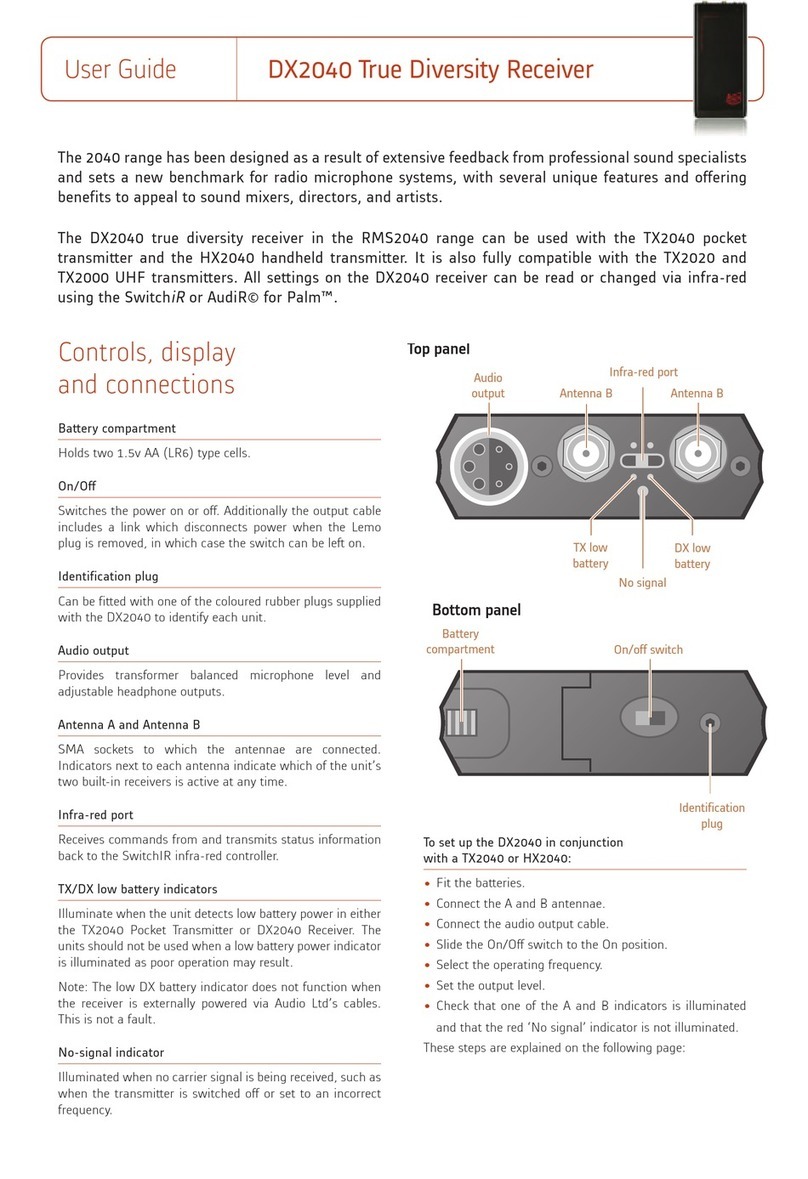
Chrontel CH7511B Guide

AN-B014
Application Note
206-1000-014 Rev. 1.7 2020-07-14 1
Chrontel
PCB Layout and Design Guide for CH7511B and CH7512B
1.0 INTRODUCTION
Chrontel’s CH7511B/7512B is an eDP/DP receiver that integrates LVDS Transmitter for the notebook/AIO display.
The CH7511B is designed to comply with the Embedded Display Port Specification 1.2 and the CH7512B is
designed to comply with the Display Port Specification 1.1a. The CH7511B/7512B provides support for two main
link lanes with data rate running at either 1.62Gb/s or 2.7Gb/s, and accepts data in 18-bit 6:6:6 or 24-bit 8:8:8 RGB
digital format. During system power-up, setting the power on/off sequence for a particular panel can be achieved
through the CH9904 Boot ROM registers. The CH7511B/7512B has incorporated a brightness control function to
interface with LCD backlight module. Brightness control commands sent through AUX Channel are dynamically
translated by the CH7511B/7512B and converted into the LCD backlight control signals.
The CH7511B/7512B can support 18-bit Single Port, 18-bit Dual Port, 24-bit Single Port and 24-bit Dual Port LVDS
outputs in both OpenLDI and SPWG bit mapping for LVDS application. The CH7511B/7512B supports LVDS
output up to 1920x1200.
This application note focuses only on the basic PCB layout and design guidelines for the CH7511B/7512B eDP/DP
Receiver with LVDS Transmitter. Guidelines in component placement, power supply decoupling, grounding, input
/output signal interface are discussed in this document.
The discussion and figures presented in this document are based on the 68-pin QFN (8x8 mm) package of the
CH7511B/7512B. Please refer to the CH7511B/7512B datasheet for details of the pin assignments.
2.0 COMPONENT PLACEMENT AND DESIGN CONSIDERATIONS
Components associated with the CH7511B/7512B should be placed as close as possible to the respective pins. The
following will describe guidelines on how to connect critical pins, as well as the guidelines for the placement and
layout of components associated with these pins.
2.1 Power Supply Decoupling
The optimal power supply decoupling is accomplished by placing a 0.1μF ceramic capacitor at each of the power
supply pins as shown in Figure 1. These capacitors (C1, C2, C3, C4, C5, C7, C8, C10, C11, and C12) should be
connected as close as possible to their respective power and ground pins using short and wide traces to minimize lead
inductance. Whenever possible, a physical connecting trace should connect the ground pins of the decoupling
capacitors to the CH7511B/7512B ground pins, in addition to ground vias.
2.1.1 Ground Pins
The CH7511B/7512B should be connected to a common ground plane to provide a low impedance return path for the
supply currents. Whenever possible, each of the CH7511B/7512B ground pins should be connected to its respective
decoupling capacitor ground lead directly, and then connected to the ground plane through a ground via. Short and
wide traces should be used to minimize the lead inductance. Refer to Table 1 for the Ground pin assignments.

CHRONTEL AN-B014
2 206-1000-014 Rev. 1.7 2020-07-14
2.1.2 Power Supply Pins
There are eleven power supply pins: AVDD, DVDD, LVDD, and VDDGPO. Refer to Table 1 for the Power supply
pin assignments. Refer to Figure 1 for Power Supply Decoupling.
Table 1: Power Supply Pin Assignments for the CH7511B/7512B (68QFN)
Pin
# of Pins
Type
Symbol
Description
7,42
2
Power
DVDD
Digital supply voltage (1.8V)
3,4,60,66,67
5
Power
AVDD
Analog supply voltage (1.8V)
18,32,52
3
Power
LVDD
LVDS driver supply voltage and GPIO
supply voltage (3.3V)
8,21,35,40,45,63,
Thermal pad
6
Ground
GND
Power ground
L1 47R 100MHz
1 2
C6
10uF
C1
0.1uF C2
0.1uF C3
0.1uF C4
0.1uF C5
0.1uF
C7
0.1uF C8
0.1uF C9
10uF
C12
0.1uF
L2 47R 100MHz
1 2
VCC3_3
VCC1_8
C11
0.1uF
C10
0.1uF L3 47R 100MHz
1 2
C13
10uF
QFN
U1
CH7511B
DVDD 7,42
LVDD 18,32,52
AVDD 3,4,60,66,67
Thermal Pad
GND 8,21,35,40,45,63
RESETB
VCC18
VCC33 T1
Figure 1: Power Supply Decoupling and Distribution

CHRONTEL AN-B014
206-1000-014Rev. 1.7 2020-07-14 3
Note:
1. Pease make sure that the voltage of LVDD (VCC33) should be supplied before the voltage of DVDD
and AVDD (VCC18).
2. The RESETB signal should be supplied to the CH7511B/7512B after the powers are stable.
3. T1 (the VCC18 rise slope time) should not be larger than 2ms.
4. The exposed pad, which is the thermal pad, must be linked to GND.
5. All the Ferrite Beads described in this document are recommended to have an impedance of less than
0.05Ω at DC; 23Ω at 25MHz & 47Ωat 100MHz. Refer to Fair Rite part #2743019447 for details (an
equivalent part can be used for the diagram).
2.2 Internal Reference Pins
• RBIAS pin
This pin sets the Band-gap Bias Voltage. A 10 KΩ, 1% tolerance resistor should be connected between RBIAS and
GND as shown in Figure 2. A smaller resistance will create less Band-gap Bias voltage. The distance between the
resistor and the CH7511B/CH7512B should be less than 6mm, the shorter and wider trace the better. For optimal
performance, this signal should not overlay the analog power or analog output signals.
R1
10K(1%)
U1
CH7511B
RBIAS 68
QFN
Figure 2: RBIAS Pin Connection
2.3 General Control Pins
• RESETB
This pin is the chip reset pin for the CH7511B/7512B. The RESETB pin is internally pulled-up. But when it is
pulled-low, this pin places the device in the power-on-reset condition. As shown in Figure 3, one 10KΩ resistor is
necessary to be pulled high to DVDD (1.8V). One 0.1uf capacitor is recommended to be pulled low to GND. After
the powers are stable, send the RESETB signal (low to high) to the chip, as shown in Figure 1.
Option1: link the RESETB signal to the external GPIO_PCH signal (1.8V).
Option2: add the level shifter circuits to link the RESETB signal to the GPIO_PCH signal (3.3V).
• XI, XO
A 27MHz crystal (30ppm) can be connected to XI and XO as the CH7511B/7512B the optional reference clock
input. In PCB design, a 27MHz crystal must be placed as close as possible to the XI and XO pins, with traces
connected from point to point, overlaying the ground plane. Since the crystal generates the timing reference for the
CH7511B/7512B, it is essential that noise not couple into these input pins.
The crystal load capacitance, CL, is usually specified in the crystal spec from the vendor. Refer to Figure 3 for a
crystal circuit reference design and an example of load capacitors.
• REFCK

CHRONTEL AN-B014
4 206-1000-014 Rev. 1.7 2020-07-14
The REFCK is another optional pin as the reference input clock for the CH7511B/7512B. A 27MHz (3.3V) clock
may be injected at this pin as shown in Figure 3. For PCB design, the capacitor must be placed as close as possible to
the REFCK pin, with traces connected from point to point, overlaying the ground plane.
U1
CH7511B
RESETB 1
XI 6
XO 5
REFCK 9
Note: The resetb is 1.8V level.
It need 10Kohm resister to 1.8V
and 0.1uf capacitor to GND.
So if the system reset signal is 3.3V,
the level shift circuit is necessary.
R3
1k
R2
10K
VCC33
RESETB_PCH
R1
10K
Q2
PMBS3904 1
2 3
Q1
PMBS3904
1
2 3
C1
0.1uF
12
VCC18
RESETB
C2
22pF
Y1
27MHz
C3
22pF
REFCK
NOTE: CH7511B supports two
kinds of clock input ways
Option1: use 27MHz crystal with 22pf
capacitors
Option 2: inject clock 27MHz(3.3V) in
REFCK pin(Pin 9)
Customer must choose one option
for CH7511B clock
Figure 3: General Control Pins
2.4 Serial Port Control Pins
• SPC0 and SPD0
SPD0 and SPC0 function as a serial interface where SPD0 is the bi-directional data and SPC0 is an input-only serial
clock. In the reference design, SPD0 and SPC0 pins are pulled up to LVDD (+3.3V) with 6.8k resistors. Through
these two pins, the internal register values of the chip can be read. The external Boot ROM can be updated if these
pins are connected to SPC1 and SPD1 with jumpers as shown in Figure 4.
• SPC1 and SPD1
SPD1 and SPC1 function as a serial interface where SPD1 is bi-directional data and SPC1 is an input only serial clock.
In the reference design, SPD1 and SPC1 pins are pulled up to LVDD (+3.3V) with 6.8kΩ resistors as shown in Figure
4.
SPD1 and SPC1 are used to interface with the CH9904 (the serial Boot ROM). The CH7511B/7512B will auto-load
the values, such as EDIDs and configurations, etc., from the Boot ROM upon power-on or reset.

CHRONTEL AN-B014
206-1000-014Rev. 1.7 2020-07-14 5
U1
CH7511B
SPC0 54
SPC1 51
SPD0 53
SPD1 50
SPC0
R2
6.8K
1 2
R1
6.8K
1 2
VCC3_3
SPD0
R6
6.8K
R5
6.8K
R810K
R4
6.8K
1 2
U2
CH9904
GP1 1
GP2 2
GP3 3
GND 4
SPD
5SPC
6WE
7VCC
8
R3
6.8K
1 2
VCC3_3VCC3_3VCC3_3
R7
6.8K
SPD1
SPC1
JP1
HEADER 1x2
1 2
JP2
HEADER 1x2
1 2
SPD0
SPC1SPC0 SPD1
CH7511B Boot Rom
Figure 4: Serial Port Control
Note: If you use SPC0/SPD0 or the AUX channel to update the CH9904 Boot ROM, the precondition is that
the MCU firmware must work properly. It is recommended that the IIC/SMBUS be used to update
CH9904, by linking the IIC/SMBUS to SPC0 and SPD0
2.5 Display Port Signal Pins
• DP0P/N, DP1P/N
These pins accept two AC-coupled differential pair signals from the Display Port transmitter.
Since the digital serial data of the CH7511B/7512B may be toggled at speeds up to 2.7 GHz, it is strongly
recommended that the connection of these video signals between the graphics controller and the CH7511B/7512B be
kept as short as possible, avoid discontinuities in the reference plane and be isolated as much as possible from the
analog outputs and analog circuitry. For optimal performance, these signals should not overlay the analog power or
analog output signals. When a signal pair has to changes layers, the ground stitching vias should be placed close to
the signal vias. A minimum of 1 to 3 stitching vias per pair of signals is recommended. Never route a trace so that it
straddles a plane split. It is recommended that 5 mils traces be used in routing these signals. There should be 7 mils
spacing between each intra pair. The length for a pair of intra differential signals should be matched within 5 mils.
The length for inter pairs should be matched within 2 inches. Bend smaller than 45 degrees should be avoided. The
AC coupling capacitors for the serial video inputs must be placed close to the GMCH, as shown in Figure 5.
GMCHCH7511
C1 0.1uF
C2 0.1uF
C3 0.1uF
C4 0.1uF
Source
DP0P 61
DP0N 62
DP1P 64
DP1N 65
DP0P
DP0N
DP1P
DP1N

CHRONTEL AN-B014
6 206-1000-014 Rev. 1.7 2020-07-14
Figure 5: CH7511B/7512B DP Main Link Lane Inputs
• AUXP and AUXN
These two pins are for Display Port AUX channel control that accepts a half-duplex, bi-directional AC-coupled
differential signal. An AC coupling capacitor, 0.1uF recommended, must be placed on the end as shown in Figure 6.
• HPDET
This output pin indicates whether the device is active or not. It also generates an interrupt pulse as defined by the
Display Port standard. Output voltage is 3.3V. A resistor, greater than 100KΩ, should be connected between this pin
and GND as shown in Figure 6.
U1
CH7511B
AUXN 43
HPDET 59
AUXP 44
U2
GMCH
AUXN
HPDET
AUXP
C1 0.1uF
C2 0.1uF
R1
100K R2
100K
Sink Source eDP
U3
CH7512B
AUXN 43
HPDET 59
AUXP 44
U4
GMCH
AUXN
HPDET
AUXP
C3 0.1uF
C4 0.1uF
R3
100K R4
100K
Source DP
Sink
C5 0.1uF
C6 0.1uF
R5
1M R6
1M R7
100K
R8
100K
+3.3V +3.3V
Figure 6: CH7511B/7512B AUX channel and HPDET
2.6 LVDS Signal Pins
• LVDS Outputs (LDCxP and LDCxN)
The LVDS output signals are LDCxP and LDCxN. The LVDS is a differential interface with a nominal swing 200mV.
The following rules should be applied to the signals:
1. Keep traces as short as possible.
2. Make these traces have 100Ω differential impedance.
3. Trace widths should be 5 mils.
4. Intra Pair spacing (spacing between the “+” and “-” pairs) should be 7mils.
5. Inter Pair spacing (spacing between one differential pair and another) should be a minimum of 20 mils
except in the area near the pins.
6. Difference in trace lengths between “+” and “-” pairs should be within 5mils.
7. Difference in trace lengths among Inter pairs should be within 10mils.
8. “+” And “-” pairs should be routed in parallel.
2.7 Other function pins

CHRONTEL AN-B014
206-1000-014Rev. 1.7 2020-07-14 7
• GLED, OLED
GLED and OLED pins output LED control signals to determine if the CH7511B/7512B is in normal or abnormal
power and mode status. If GLED has output (3.3V), the CH7511B/7512B is in normal status. If OLED has output
(flickers from 0 or 3.3V), the CH7511B/7512B is in abnormal status. The design is shown in Figure 7.
GLED 57
OLED 58
CH7511
GLED
D2
P504CT-ND
R4
100
1
32
Q2
BSS138CT-ND
D1
P504CT-ND
R2
100
+3.3V
+3.3V
1
32
Q1
BSS138CT-ND
R3
10k
GLEDGLEDGLEDGLEDGLEDGLEDGLEDGLEDGLEDGLEDGLEDGLED
OLEDOLED
R1
10k
Figure 7: LED Control
• BLUP, BLDN
1. BLUP is the increase backlight brightness input pin.
2. BLDN is the decrease backlight brightness input pin.
Buttons can be placed at these pins to adjust the backlight brightness. The design is shown in Figure 8.
• PWRDN
The CH7511B/7512B enters into or exits power down state when receiving an active low pulse from this pin. The
connection is shown in Figure 8.

CHRONTEL AN-B014
8 206-1000-014 Rev. 1.7 2020-07-14
BLDN
55
BLUP
56
PWRDN
41
R1
10K
SW1 BLDN
+3.3V
R5
10K
SW3
+3.3V
PWRDN
BLUP
C1
0.1uF
R2
10K
BLUPBLUPBLUPBLUPBLUPBLUP
R3
10K
SW2
C2
0.1uF
+3.3V
C3
0.1uF
R6
10K
R4
10K
CH7511
Figure 8: BLDN, BLUP and PWRDN Connections
• GPIO [0:3]
These pins can be used as panel select signals. They can be pulled high or low forming into 16 different combinations.
Every combination can match with one panel type. The connection is shown in Figure 9.
R2
10K
R3
10K
R4
10K
R6
100
R7
100
R8
100
R5
100
GPIO[3]
GPIO[2]
GPIO[1]
GPIO[0] 33
GPIO[1] 34
GPIO[2] 37
GPIO[3] 38
U1
CH7511
GPIO[0]
R1
10K
LVDD(+3.3V)
Figure 9: GPIO [0:3] connections
Method 1 (default)
GPIO [3:0] can be connected to high/low level by pull-up/pull-down resistors on the CH7511B/7512B PCB board;
The CH7511B/7512B can obtain the correct LVDS Panel selection value upon power ON or reset. As shown in
Figure 10, if the customer don’t want to change MB, they can they the GPIO[0:3] in LCD inverter to identify
different panel.

CHRONTEL AN-B014
206-1000-014Rev. 1.7 2020-07-14 9
Figure 10: Typical application to control the CH7511B/7512B GPIO[3:0]
Method 2
GPIO [3:0] can be controlled by another chip’s GPIO pins in the CH7511B/7512B application system. If the chip
controlling the CH7511B/7512B GPIO [3:0] cannot set the expected value before the CH7511B/7512B finishes
loading its firmware (typically 100ms after the CH7511B/7512B is powered ON), the controlling chip must reset the
CH7511B/7512B for it to load the Boot ROM file again. It is recommended that the CH7511B/7512B be reset by the
controlling chip each time the LVDS Panel selection value is changed.
Figure 11 shows the typical cases to control the CH7511B/7512B GPIO [3:0] by another chip. Case 1 is the right
loading case, in which the GPIO pins remains stable within 100ms after reset. Case 2 is the wrong loading case, in
which the GPIO value, represented by the GPIO pins, is still at random after the firmware is completely loaded.
Therefore, the reset signal must be given again. The reset pulse width of larger than 10ms is recommended.
RESETB
Loading FirmwareIDLE Loading LVDS
Configurations
CH7511 I2C
Master Activity
Random Values Correct LVDS Panel Selection Value
IDLE
CH7511 GPIO[3:0]
Case 1: CH7511 GPIO[3:0] settles before it starts loading LVDS configurations
RESETB
Loading Firmware
IDLE Loading LVDS
Configurations
CH7511 I2C
Master Activity
Random Values Correct LVDS Panel Selection Value
IDLE
CH7511 GPIO[3:0]
Case 2: CH7511 GPIO[3:0] cannot settle before it starts loading LVDS configurations
Loading Firmware Loading LVDS
Configurations
Wrong LVDS
configurations! Correct LVDS
configurations!
Reset pulse generated by
Customers host chip
Figure 11: Typical cases to control CH7511B/7512B GPIO [3:0] by host chip

CHRONTEL AN-B014
10 206-1000-014 Rev. 1.7 2020-07-14
Note:
1. The GPIO pins must remain stable for its corresponding value within 100ms after reset. Otherwise, a
reset signal must be given again.
2. The firmware loading must be completed before VBIOS starts to function. Otherwise, some BIOS
images may be lost.
• PWM_OUT0, PWM_OUT1
The output Frequency from PWM_OUT0 can be up to 400 KHz. Its duty cycle ranges from 0% to 100%.
Alternatively, the PWM bypass mode may be used to output the PWM signal through this pin. The voltage level is
3.3V.
The output Frequency from PWM_OUT1 can be up to 400 KHz. Its duty cycle ranges from 30% to 100%. The
voltage level is 3.3V.
Customers may choose PWM_OUT0 or PWM_OUT1 in their application. Refer to the datasheet for detailed
information.
• PWM_IN
PWM_IN has two working modes: Bypass mode and Duty Cycle Multiplication with AUX CH mode. In bypass
mode, the input frequency to PWM_IN can be up to 1MHz. In Duty Cycle Multiplication with the AUX CH mode,
the input frequency to PWM_IN can be up to 50 KHz. In either mode, the voltage level is 3.3V.
U1
CH7511B
ENAVDD 47
IRQ 36
PWM_OUT0 48
PWM_OUT1 39
PWM_IN 49
JP1
HEADER 1x2
1 2
R1 0
R2 0PWM_OUT
PWM_IN
Figure 12: PWM and IRQ Control connections
• IRQ
IRQ (pin 36) can output an interrupt signal when the BLUP and BLDN are executing and should be connected to
ENAVDD pin as shown in Figure 12.
• Reserved
Reserved pin (pin 2) should be left open in the application.
2.8 Important Design Considerations
(Panel power, backlight power, pull-up voltage)
• LVDS Power
Close attention must be paid to the power supplied to the LVDS backlight and the LVDS panel. Power requirements
may differ from panel to panel. Please check the panels’ power and backlight voltage specifications. The ENABKL
and ENAVDD may be used to control the power for the LVDS backlight and the LVDS logic circuitry.

CHRONTEL AN-B014
206-1000-014Rev. 1.7 2020-07-14 11
• Signal Wires, POWER and GND layout
Do not layout the wire or VIAs between the exposed thermal pad and the pin pads. Refer to Figure 13.
1
2
3
4
5
6
7
8
9
10
11
12
13
14
15
16
17
18
19
20
21
22
23
24
36
35
34
48
47
46
45
44
43
42
41
40
39
38
37
25
26
27
28
29
32
31
30
64
63
62
61
60
59
58
57
56
55
54
53
52
49
50
51
33
65
66
67
68
Thermal exposed pad
Figure 13: Wires or vias are not allowed in these four areas
2.9 Thermal Exposed Pad Package
The CH7511B/7512B is available in a 68-pin QFN package with exposed thermal pad. The advantage of the exposed
thermal pad package is that the heat can be dissipated through the ground layer of the PCB more efficiently. When
properly implemented, the exposed thermal pad package provides a means of reducing the thermal resistance of the
CH7511B/7512B. Careful attention to the design of the PCB layout is required for good thermal performance. For
maximum heat dissipation, the exposed thermal pad of the package should be soldered to the PCB as shown in Figure
14.
Die
Exposed Pad
Solder
PCB
Pin
Figure 14: Cross-section of exposed thermalpad package

CHRONTEL AN-B014
12 206-1000-014 Rev. 1.7 2020-07-14
3.0 REFERENCE DESIGN EXAMPLE
The following schematics are to be used as a CH7511B/7512B PCB design example only. It is not a complete design.
Those who are seriously doing an application design with the CH7511B/7512B and would like to have a complete
reference design schematic should contact Applications within Chrontel, Inc.
3.1 Schematics of Reference Design Example

CHRONTEL AN-B014
206-1000-014Rev. 1.7 2020-07-14 13
JP10
HEADER 1x2
1 2
SPC0 SPC1
SPD0 JP11
HEADER 1x2
1 2 SPD1
GLED
VCC18
JP12
HEADER 1x2
1 2
D1
P504CT-ND
ENAVDDIRQ
R16
100
Q3
BSS138CT-ND
1
32
D2
P504CT-ND
R17
100
Must be reserv ed, Jumpe r canbe
repla ce with 0 ohm r esisitor
+3.3V +3.3V
Q4
BSS138CT-ND
1
32
DP0N
R15
1k
R48
100
A2M A2P
GPIO[2]GPIO[2]
HPDET
GND
C3 0.1uF
U4
CH9904(SOIC-8package)
GP2
2
GP3
3
GND
4SPD 5
SPC 6
WE 7
VCC 8
GP1
1
C24
22pF
GND
R36
6.8k
Q6
MMBT3904
1
2 3
U5
SI4953
S1
1
G1
2
S2
3
G2
4D2 5
D2 6
D1 7
D1 8
C1 0.1uF
Q5
H2N7002
1
32
R37
470
R3
10K
SW2
SPD0
U7
SI4953
S1
1
G1
2
S2
3
G2
4D2 5
D2 6
D1 7
D1 8
+3.3V
SPD0
BLDN
Y1
27MHz
DP0P
R8 50
R14
100K
Q8
MMBT3904
1
2 3
R50
10k
R56
470
C4 0.1uF
R13
10K(1%)
R38
6.8k
U2
DP_sink
ML_Lane3n
1GND 2
ML_Lane3p
3ML_Lane2n 4
GND
5ML_Lane2p 6
ML_Lane1n
7GND 8
ML_Lane1p
9ML_Lane0n 10
GND
11 ML_Lane0p 12
GND
13 GND 14
AUX_CHp
15 GND 16
AUX_CHn
17 HPDET 18
RTN_DPPWR
19 DPPWR 20
GND
22
GND
23
GND
24
GND
25
C23
0.1uF
Q7
H2N7002
1
32
A7M
A7P
GND
R51
100
U3
CH7511B
RESETB
1
Reserved
2
AVDD
3
AVDD
4
XO
5
XI
6
DVDD
7
GND
8
REFCK
9
LL2CP
10
LL2CN
11
LDC7P
12
LDC7N
13
LDC6P
14
LDC6N
15
LDC5P
16
LDC5N
17
LVDD
18
LDC4P
19
LDC4N
20
GND
21
LDC3P
22
LDC3N
23
LL1CP
24
LL1CN
25
LDC2P
26
LDC2N
27
LDC1P
28
LDC1N
29
LDC0P
30
LDC0N
31
LVDD
32
GPIO[0]
33
GPIO[1]
34
SPC1 51
SPD1 50
PWM_IN 49
PWM_OUT0 48
ENAVDD 47
ENABKL 46
GND 45
AUXP 44
AUXN 43
DVDD 42
PWRDN 41
GND 40
PWM_OUT1 39
GPIO[3] 38
GPIO[2] 37
IRQ 36
GND 35
RBIAS 68
AVDD 67
AVDD 66
DP1N 65
DP1P 64
GND 63
DP0N 62
DP0P 61
AVDD 60
HPDET 59
OLED 58
GLED 57
BLUP 56
BLDN 55
SPC0 54
SPD0 53
LVDD 52
VCC33
CLK1M CLK1P
R39
50k
GPIO[3]
JP1
HEADER 3
1
23
R58
10k
R10
6.8k
R7
10K
GPIO[3]GPIO[3]
R9
6.8k
R57
50k
R11
10K
C26
22pF
C2 0.1uF
R35
1.8k
JP2
HEADER 3
1
23
+3.3V +3.3V
+3.3V
VCC18
+5V+3.3V
+3.3V
SPC1
+5V+3.3V
GPIO[2]A6M
A6P
A5M
A5P
C14
0.1uF
R1
10K
+3.3V
SW3
+3.3V
PWRDN
A4P
R23
10k
OLEDOLED
SPD0
IRQ
IRQ
A4M
PWM_OUT0
R28 0
PWM_OUT
R29 0
PWM_OUT
NO TE : PW M_ O UT 0 (0 ~ 100 % d u ty cy c le or PW M b ypa s s
mode)
PW M_ O UT 1 (30 ~1 0 0% du t y c y cl e)
PWM_OUT1
PWM_OUT0
Solde r o ption
R22
10k
GLEDGLEDGLEDGLEDGLEDGLED
SPD0
C5
0.1uF
+3.3V
A3P
L1
Bead
GND
C7
10uF
+1.8V
U1
IRU1206-18
Vout
3Gnd
2Vin
1
pin 4
C8
0.1uF
NO TE : Cu st o me r ca n c h oo s e
di ff e re n t p ane l b y p ul l
hi gh or lo w of G P IO [ 0:3 ].
L2
Bead
C6
10uF
R32
6.8k
VCC18
A3M
GND
NO TE : Cu st o me r is b e tte r t o l ink
sp c0 and sp d0 to SMB US/ IIC to
up da t e t h e Bo o t R O M lat e r
CLK1M
CLK1P
AUXP
AUXN
GND
GND
GND
GND
GND
HPDETHPDET
GND
GND
GNDGNDGNDGNDGNDGND
DPPWR
GNDGNDGND
GPIO[0]
GPIO[0]
R27
100
A2M
A2P
RESETB_PCH
R26
100
PWM_OUT1
C19
0.1uF
C12
0.1uF C16
0.1uF
Backlight
C13
0.1uF C15
0.1uF
VCC18
ENABKL
VCC33
C18
0.1uF
VCC33
A1M
A1P
Note: The r esetb is 1.8V
level .
It need 10 Kohm resister to
1.8V
and 0.1uf cap acitor to GN D.
So if th e system reset sig nal
is 3. 3V,
the leve l shift circ uit is
necessary.
BLUP
R20
10K
DP1N
A0M
A0P
R21
10K
NOTE:
1. The dotted line partsare option funtion circuits.
2. The voltage circuit can only support CH7511B chip
to work.If supporting the panel voltage, please add the
other circuit.
3. Whether to use PWM_IN(3.3V), PWM_OUT0(3.3V)
and PWM_OUT1(3.3V) is determined by customers.
Which isused for Panel luminance adjustment.
4. DP and LVDS diffential pairsshould be asshort as
possible. Please see appliciton note for detial layout guide
5. The CH7511B thermal exposed pad must be linked to
GND
GPIO[0]
DP1P
SPD1
VCC33
VCC PanelDriver
ENAVDD
CH7511B Boot Room
GND
A3M R53
100 A3P
C17
0.1uF
GPIO[1]
GPIO[1]
BLUP
C20
0.1uF
R12
10K
R18
10K
C10
0.1uF
R5
10K
VCC18
VCC33
R19
10K
IRQ
C21
0.1uF
GPIO[1]
GPIO[2]
GPIO[2]
NO TE : If t h e s ouc e o f A UX ha s
0. 1u F ca p, pl e as e do n' t ad d
ca p i n C H75 1 1 por t . For AU X C H
Ci rc u it , Pl ea s e r efe r t o A N
an d D P S pec
NOTE: CH7511B supports two kinds of clock input ways
Option1: use 27MHz crystal with 22pf capacitors
Option 2: inject clock 27MHz (3.3V) in REFCK pin(Pin 9)
Customer must choose one option for CH7511 clock
DP0P
R2
10K
BLUPBLUPBLUP
SW1
C9
0.1uF
A0M
DP0N
C22
0.1uF
PWM_IN
A6M
OLED
R49
100
GPIO[3]
GPIO[3]
A6P
A7M R52
100
CLK2M
A7P
CLK2P
R54
100
A4M R41
100
A5M
A4P
R43
100 A5P
R40
100
Q2
PMBS3904
1
2 3
BLDN
R34
6.8k
R33
6.8k
+3.3V
DP1N
DP1P
VCC33
R24
100
ENAVDD
REFCKREFCK
SPC1
ENABKL
SPC0
C11
0.1uF
R6
10K
GLED
SPD1
Power
Supply
GND
PWRDN
RESETB
GPIO[0]GPIO[0]
VCC18
R4
10K
Q1
PMBS3904
1
2 3
HPDET
+3.3V
R25
100
SPC0
VCC18VCC18
Panel Voltage and backlight control circuit
DP Interface
AUXP
C25 0.1uF
C27 0.1uF
AUXN
VCC18
VCC18
A0P
VCC18
CLK2P
GPIO[1]GPIO[1]
HPDET A1M R42
100 A1P
SPC0
SPC0
CLK2M
Figure 13: CH7511B/7512B Reference schematic

CHRONTEL AN-B014
14 206-1000-014 Rev. 1.7 2020-07-14
3.2 Reference Board Preliminary BOM
Table 2: CH7511B/7512B Reference Design BOM List
Item
Quantity
Reference
Part
1
23
C1, C2, C3, C4, C5, C8, C9, C10, C11, C12, C13, C14,
C15, C16, C17, C18, C19, C20, C21, C22,
C23, C25, C27
0.1uF
2
2
C6, C7
10uF
3
2
C24, C26
22pF
4
2
D1, D2
P504CT-ND
5
2
JP1, JP2
HEADER 3
6
3
JP10, JP11, JP12
HEADER 2
7
2
L1, L2
Bead
8
2
Q1, Q2
PMBS3904
9
2
Q3, Q4
BSS138CT-ND
10
2
Q5, Q7
H2N7002
11
2
Q6, Q8
MMBT3904
12
17
R1, R2, R3, R4, R5, R6, R7, R11, R12, R18,
R19, R20, R21, R22, R23, R50, R58
10K
13
1
R8
50
14
7
R9, R10, R32, R33, R34, R36, R38
6.8k
15
1
R13
10K(1%)
16
1
R14
100K
17
1
R15
1K
18
16
R16, R17, R24, R25, R26, R27, R40, R41, R42,
R43, R48, R49, R51, R52, R53, R54,
100
19
1
R35
1.8k
20
2
R37, R56
470
21
2
R39, R57
50k
22
2
R28, R29
0
23
3
SW1, SW2, SW3
P8058SS-ND
24
1
U1
IRU1206-18
25
1
U2
DP_Sink
26
1
U3
CH7511B/7512B
27
1
U4
CH9904 (SOIC-8)
28
2
U5, U7
SI4953
29
1
Y1
27MHz
4.0 REVISION HISTORY
Table 3: Revisions
Rev.
#
Date
Section
Description

CHRONTEL AN-B014
206-1000-014Rev. 1.7 2020-07-14 15
1.0
04/19/2012
All
Layout Guide and Design Guide for CH7511B and CH7512B release.
1.1
11/29/2013
2.3
2.5
Add demand of RBIAS
Add demand of DP layout
1.2
03/11/2014
2.5
3.1
Modify Aux reference schematic
Update reference schematic
1.3
10/13/2014
2.4
2.6
2.7
3.1
Modify SPC0, SPC1, SPD0, SPD1 schematic
Modify demand of LVDS layout rules
Modify IRQ schematic
Update reference schematic
1.4
11/11/2014
All
Technical and grammatical review
1.5
01/27/2015
2.4
Modify description of SPC1 and SPD1
1.6
04/18/2016
2.3
2.4
Modify Reset
Modify SPC1 and SPD1
1.7
07/14/2020
Disclaimer
Update the disclaimer

CHRONTEL AN-B014
16 206-1000-014 Rev. 1.7 2020-07-14
Disclaimer
This document provides technical information for the user. Chrontel reserves the right to make changes at any time
without notice to improve and supply the best possible product and is not responsible and does not assume any
liability for misapplication or use outside the limits specified in this document. CHRONTEL warrants each part to be
free from defects in material and workmanship for a period of one (1) year from date of shipment. Chrontel assumes
no liability for errors contained within this document. The customer should make sure that they have the most recent
data sheet version. Customers should take appropriate action to ensure their use of the products does not infringe
upon any patents. Chrontel, Inc. respects valid patent rights of third parties and does not infringe upon or assist others
to infringe upon such rights.
Chrontel PRODUCTS ARE NOT AUTHORIZED FOR AND SHOULD NOT BE USED WITHIN LIFE SUPPORT
SYSTEMS OR NUCLEAR FACILITY APPLICATIONS WITHOUT THE SPECIFIC WRITTEN CONSENT OF
Chrontel. Life support systems are those intended to support or sustain life and whose failure to perform when used
as directed can reasonably expect to result in personal injury or death.
Chrontel
www.chrontel.com
2020 Chrontel - All Rights Reserved.
This manual suits for next models
1
Table of contents
