Clarion ARX850z User manual

-1- ARX8570z
Published by Service Dept.
Printed in Japan
Clarion Co., Ltd.
ExportDivision-22-3,Shibuya2-chome,Shibuyaku,Tokyo,150-8335Japan Tel:03-3400-1121
ServiceDept.-50kamitoda,Toda-shi,Saitama,335-8511Japan Tel:048-443-1111 FAX:048-433-6996 298-5718-00 Jan.1999 P
Service Manual
Model
AM/FM Cassette Player with
CD/MD Changer Control
(PE-1637B)
■SPECIFICATIONS
FM tuner
Frequency range: 87.9MHz to 107.9MHz
Usable sensitivity: 11dBf
50dB quieting sensitivity:
17dBf
Alternate channel selectivity:
75dB
Stereo separation(1kHz):
35dB
Frequency response(±3dB):
30Hz to 15kHz
AM tuner
Frequency range: 530kHz to 1710kHz
Usable sensitivity: 25μV
Tape deck
Wow & flutter(WRMS): 0.06%
Channel separation(1kHz):
45dB
Frequency response(±3dB):
120μs(Normal)
30Hz to 18kHz
70μs(CrO2,FeCr,Metal)
30Hz to 20kHz
S/N ratio: 70μs(CrO2,FeCr,Metal)
Dolby NR off 58dB
Dolby B NR 67dB
Dolby C NR 74dB
Audio
Maximum power output:
180W(45W×4ch)(EIAJ)
Continuous average power output:
17W×4,into 4Ω,
20Hz to 20kHz,1%THD
Bass control action(30Hz):
±15dB
Treble control action(10kHz):
±10dB
Line output level(0VU tape):
1.6V
General
Power supply voltage: 14.4V DC(10.8 to 15.6V allowable)
negative ground
Current consumption: Less than 15A
Speaker impedance: 4Ω(4Ωto 8Ωallowable)
Dimensions(mm): Source unit
178(W)×50(H)×155(D)
Remote control unit
44(W)×110(H)×27(D)
Weight: Source unit 1.6kg
Remote control unit
30g(including battery)
※Dolby noise reduction manufactured under license from
Dolby Laboratories Licensing Corporation
Dolby and the double-D symbol are trademarks of Dolby
Laboratories Licensing Corporation.
※Specifications and design are subject to change with-
out notice for further improvement.
■NOTE
※We cannot supply PWB with component parts in prin-
ciple. When a circuit on PWB has failure , please repair
it by component parts base. Parts which are not men-
tioned in service manual are not supplied.
■COMPONENTS
PE-1637B-A
Main unit −−−−− 1
-2-
ARX8570z
■To engineers in charge of repair
or inspection of our products.
Before repair or inspection, make sure to follow
the instructions so that customers and Engineers
in charge of repair or inspection can avoid suf-
fering any risk or injury.
1. Use specified parts.
The system uses parts with special safety features
against fire and voltage. Use only parts with equivalent
characteristics when replacing them.
The use of unspecified parts shall be regarded as re-
modeling for which we shall not be liable. The onus of
product liability (PL) shall not be our responsibility in
cases where an accident or failure is as a result of un-
specified parts being used.
2. Place the parts and wiring back in their original positions
after replacement or re-wiring.
For proper circuit construction, use of insulation tubes,
bonding,gaps to PWB, etc, is involved. The wiring con-
nection and routing to the PWB are specially planned
using clamps to keep away from heated and high volt-
age parts. Ensure that they are placed back in their origi-
nal positions after repair or inspection.
Remote control RCB-130-600 1
Battery(SUM-3) −−−−− 2
Mounting bracket 300-7742-00 1
DCP case 335-6035-20 1
Outer escutcheon 370-5771-00 1
Extension lead 854-6349-50 1
Parts bag −−−−−
Removal tool 331-2497-00 2
Screw 716-0496-01 1
If extended damage is caused due to negligence during
repair, the legal responsibility shall be with the repairing
company.
3. Check for safety after repair.
Check that the screws, parts and wires are put back se-
curely in their original position after repair. Ensure for
safety reasons there is no possibility of secondary
ploblems around the repaired spots.
If extended damage is caused due to negligence of re-
pair, the legal responsibility shall be with the repairing
company.
4. Caution in removal and making wiring connection to the
parts for the automobile.
Disconnect the battery terminal after turning the ignition
key off. If wrong wiring connections are made with the
battery connected, a short circuit and/or fire may occur.
If extensive damage is caused due to negligence of re-
pair, the legal responsibility shall be with the repairing
company.
5. Cautions regarding chips.
Do not reuse removed chips even when no abnormality
is observed in their appearance. Always replace them
with new ones. (The chip parts include resistors, capaci-
tors, diodes, transistors, etc). The negative pole of tan-
talum capacitors is highly susceptible to heat, so use
special care when replacing them and check the opera-
tion afterwards.
6. Cautions in handling flexible PWB
Before working with a soldering iron, make sure that the
iron tip temperature is around 270℃. Take care not to
apply the iron tip repeatedly(more than three times)to
the same patterns. Also take care not to apply the tip
with force.
7. Turn the unit OFF during disassembly and parts replace-
ment. Recheck all work before you apply power to the
unit.
■ERROR DISPLAYS
If an error occurs,one of the following displays is displayed.
Take the measure described below to eliminate the problem.
Tape
CD
CHANGER
MD
CHANGER
Error display
ERROR 1
ERROR 2
ERROR 4
ERROR 8
ERROR 2
ERROR 3
ERROR 6
ERROR H
EEROR 2
ERROR 3
ERROR 6
Cause
Tape cannot be played due to defective tape
such as cut tape.
Tape is caught and cannot be played.
Tape mode cannot be detected.
Tape is caught and cannot be ejected.
A CD inside the CD changer is not loaded.
A CD inside the CD changer cannot be played
due to scratches,etc.
A CD inside the CD changer cannot be played
because it is loaded upside-down.
Displayed when the temperature in the MD
changer is too high and playback has been
stopped automatically.
An MD inside the MD changer is not loaded.
An MD inside the MD changer cannot be
played due to scratches,etc.
An MD inside the MD changer cannot be
played because it is loaded upside-down.
Displayed when a non-recorded MD is loaded
in the MD changer.
Measure
Eject the tape then replace it with a new one.
Remove the caught or wound tape.
This is a failure of tape mechanism.
Eliminate the reason for which the tape is caught.
This is a failure of CD changer's mechanism.
Replace with a non-scratched,non-warped-disc.
Eject the disc then reload it properly.
Lower the surrounding temperature and wait for a
while to cool off MD changer.
This is a failure of MD changer's mechanism.
Replace with a non-scratched,non-warped-disc.
Eject the disc then reload it properly.
Load a pre-recorded MD in the MD changer.
If an error other than the ones described above appears,press the reset button.

-3- ARX8570z
Item Procedure Measuring
instrument
■CHANGING THE RECEPTION AREA
This unit is initially set to USA frequency intervals of 10kHz
for AM and 200kHz for FM.When using it outside the
USA,the frequency reception range can be switched to the
intervals below.
Setting the reception area
1. Press BND button and select the desired radio band(FM
or AM).
2. While pressing RDM button,each time you press and
hold the number "1" of the Preset buttons for 2 seconds
or longer,the reception area switches from inside the
USA to outside the USA or from outside the USA to
inside the USA.
*Any station preset memories are lost when the recep-
tion area is changed.
■TROUBLESHOOTING
Problem
Nothing happens when
buttons are pressed.
Display is not accurate.
Cause
The microprocessor has malfunctioned
due to noise,etc.
Solution
Turn off the power,then press the OPEN button and
remove the DCP.
Press the reset button for about 2 seconds with a
thin rod. R e s e t b u tto n
■ADJUSTMENT
Dolby level 1. Playback a Dolby level test tape(400Hz,200nWb/m) and connect the Milli-volt
meter to TP101(L)/TP102(R).
2. Adjust VR101(L)/VR102(R) to obtain an output of TP101(L)/TP102(R) is 388mV
±1dB.(Dolby SW:off)
Dolby test tape
Milli-volt meter
Azimuth
adjustment 1. Playback a azimuth test tape(10kHz,−10VU) and turn each azimuth-adjusting
screw to make each FOW & REV Maximum.
2. After adjustment,make adhesion with bond.
Azimuth test tape
Milli-volt meter
Tape speed 1. Playback a Wow & flutter test tape(3kHz,−10VU) and connect the frequency
counter to TP101(L) or TP102(R).
2. Adjust Speed VR of the motor to obtain an output of TP101(L),TP102(R) is
3000Hz±45Hz.
Wow & flutter test
tape
Frequency counter
■EXPLANATION OF IC
■M30622M8-189GP 052-3344-00 Tuner/Cassette Controller
(Ce-NET)
1. Outward Form : 100 pins QFP
2. Function : GFC-3C cassette mechanism control, PLL IC control, Elec-
tric volume IC control, Ce-NET
3. Terminal Description
pin 1 : N.C. : IN : Not in use.
pin 2 : N.C. : O : Not in use.
pin 3 : APC SENSE : O : "L"= Play, "H"= FF/REW
pin 4 : N.C. : IN : Not in use.
pin 5 : TIME BASE : IN : Time base signal input terminal.
pin 6 : BYTE : IN : Connect to ground.
pin 7 : CNVSS : IN : Connect to ground.
pin 8 : N.C. : IN : Not in use.
pin 9 : N.C. : O : Not in use.
pin 10 : RESET_ : IN : Reset signal input. Negative logic.
pin 11 : X OUT : O : Crystal connection.
pin 12 : VSS : - : Ground.
pin 13 : X IN : IN : Crystal connection.
pin 14 : VCC : - : Positive supply voltage.
pin 15 : N.C. : IN : Not in use.
pin 16 : ACC DET : IN : ACC ON signal input.
pin 17 : B/U DET_ : IN : "L"= Backup OFF
pin 18 : KEY INT_ : IN : Interrupt signal input of FUNC/EJECT key
and DCP take off switch.
pin 19 : 27pinCONNECT: IN : Connect to pin 27.
pin 20 : N.C. : IN : Not in use.
pin 21 : N.C. : IN : Not in use.
pin 22 : N.C. : O : Not in use.
pin 23 : DISP RESET : O : Display IC reset signal output.
pin 24 :PULSE DIMM : O : Pulse dimmer / Back light LED ON signal
output.
pin 25 : N.C. : IN : Not in use.
pin 26 : N.C. : O : Not in use.
pin 27 : IE BUS RX : IN : IE Bus communication line.
pin 28 : IE BUS TX : O : IE Bus communication line.
pin 29 : N.C. : O : Not in use.
pin 30 : N.C. : IN : Not in use.
pin 31 : INITIAL OUT : O : Memory clear signal output to EEPROM.
pin 32 : PLL CE : O : PLL chip enable signal output.
pin 33 : PLL DO : O : PLL serial data output.
pin 34 : PLL DI : IN : PLL serial data input.
pin 35 : PLL SCK : O : PLL serial clock output.
pin 36 : FM STEREO : IN : FM stereo detection signal input.
pin 37 : NON FADER 1 : O : Non fader volume control signal output.
Ref. Table 1.
pin 38 : NON FADER 2 : O : Non fader volume control signal output.
Ref. Table 1.
pin 39 : NON FADER 3 : O : Non fader volume control signal output.
Ref. Table 1.
pin 40 : INITIAL 1 : IN : Destination setting terminal. Ref. Table 2.
pin 41 : INITIAL 2 : IN : Destination setting terminal. Ref. Table 2.
pin 42 : VOLUME CLK : O : Serial clock output to Electric volume.
pin 43 : VOLUME DO : O : Serial data output to Electric volume.
pin 44 : TONE BYPS_ : O : Tone bypass ON signal output. Negative
logic.
pin 45 : N.C. : O : Not in use.
pin 46 : DOLBY ON_ : O : Dolby ON signal output. Negative logic.
pin 47 : DOLBY B/C : O : "L"= Dolby C, "H"=Dolby B.
pin 48 : POWER M 1 : O : Power motor control signal output.
Ref. Table 3.
pin 49 : POWER M 2 : O : Power motor control signal output.
Ref. Table 3.
pin 50 : FWD/REV : O : "L"= FWD, "H"= REV.
pin 51 : N.C. : O : Not in use.

-4-
ARX8570z
pin 52 : APC DETECT_ : IN : "H"= Interval.
pin 53 : TAPE IN : IN : "H"= Tape loading start.
pin 54 : BIT 2 : IN : Mechanism mode switch signal input.
Ref. Table 4.
pin 55 : BIT 1 : IN : Mechanism mode switch signal input.
Ref. Table 4.
pin 56 : BIT 3 : IN : Mechanism mode switch signal input.
Ref. Table 4.
pin 57 : N.C. : O : Not in use.
pin 58 : REEL PULSE : IN : Reel pulse input terminal.
pin 59 : MAIN MOTOR : O : Main motor ON signal output.
pin 60 : VCC : - : Positive supply voltage.
pin 61 : MECH ON : O : Power supply control signal output for the
tape mechanism. "H"= ON.
pin 62 : VSS : - : Ground.
pin 63 : N.C. : IN : Not in use.
pin 64 : N.C. : IN : Not in use.
pin 65 : N.C. : IN : Not in use.
pin 66 : N.C. : IN : Not in use.
pin 67 : N.C. : IN : Not in use.
pin 68 : N.C. : IN : Not in use.
pin 69 : NAVI MUTE : O : Mute signal output for the audio signal of
Navigation.
pin 70 : N.C. : IN : Not in use.
pin 71 : 5V REM : O : 5V power supply ON signal output for Mi-
cro computer.
pin 72 : KEY ILL REM : O : Key illumination ON signal output.
pin 73 : AMP MUTE : O : Mute signal output to Power Amplifier.
pin 74 : SYS MUTE_ : O : System mute signal output. Negative logic.
pin 75 : LINE MUTE : O : Mute signal output for Audio signal of Ce-
NET.
pin 76 : BUS IN/OUT : O : Ce-NET audio bus select signal output.
pin 77 : SYS ACC : O : ACC detect signal output to slave micro
computer.
pin 78 : AMP REM DET_: IN : Input "L" when the remote line is shorted.
pin 79 : AMP REM OUT : O : Amplifier ON signal output terminal.
pin 80 : AUTO ANT : O : Motor antenna ON signal output terminal.
pin 81 : PHONE INT : IN : Telephone interrupt signal input.
pin 82 : N.C. : IN : Not in use.
pin 83 : N.C. : IN : Not in use.
pin 84 : N.C. : IN : Not in use.
pin 85 : N.C. : IN : Not in use.
pin 86 : N.C. : IN : Not in use.
pin 87 : N.C. : O : Not in use.
pin 88 : N.C. : O : Not in use.
pin 89 : N.C. : IN : Not in use.
pin 90 : N.C. : IN : Not in use.
pin 91 : N.C. : IN : Not in use.
pin 92 : ILL DET_ : IN : Illumination ON signal input. Negative logic.
pin 93 : N.C. : IN : Not in use.
pin 94 : A VSS : - : Ground terminal for A/D converter.
pin 95 : KEY A/D : IN : Input terminalofA/D converter for Key judg-
ment. Ref. Table 5.
pin 96 : VREF : IN : Reference voltage input for A/D converter.
pin 97 : A VCC : - : Positive supply voltage for A/D converter.
pin 98 : N.C. : IN : Not in use.
pin 99 : N.C. : O : Not in use.
pin100 : N.C. : O : Not in use.
Table 1. Non fader volume control signal output
ATT N-F 1 (pin37) N-F 2 (pin38) N-F 3 (pin39)
0 L L L
1 L L H
2 L H L
3 L H H
4 H L L
5 H L H
6 H H L
7 H H H
Table 2. Destination setting
U.S.A. Third area Japan
Initial 1 (pin40) H L Don't care
Initial 2 (pin41) L L H
Table 3. Power motor control signal output
Mechanism Mode Power M 1 (pin48) Power M 2 (pin49)
Loading head shift forward H L
Eject head go back L H
Brake H H
Stop L L
Table 4. Mechanism mode switch signal input
Mechanism Mode bit 1(pin55) bit 2(pin54) bit 3(pin56)
Eject H H H
Loading H H L
Stop L H L
FWD FF (REV REW) L L H
FWD REW (REV FF) H L L
FWD Play H L H
REV Play L H H
Table 5. A/D converter for Key judgment (pin95)
Judgment A/D steps
Eject key 0/256 to 25/256
Function key 26/256 to 51/256
With DCP (type A/B) 205/256 to 221/256
With DCP (Deck) 222/256 to 238/256
Without DCP 239/256 to 256/256
■M30622MC-176GP 052-7039-00 CD MD CA Display and
Keys (Ce-NET)
1. Outward Form : 100 pins QFP
2. Function : LCD display control, Key scan, Ce-NET communication
3. Terminal Description
pin 1 : N.C. : IN : Not in use.
pin 2 : CONTRAST : O : LCD Contrast control signal output. (Ana-
log signal)
pin 3 : DISP 5V REM : O : Power supply ON signal output for Display.
pin 4 : N.C. : IN : Not in use.
pin 5 : REMOCON : IN : Remote controller signal input terminal.
pin 6 : BYTE_ : IN : Input "L" at single mode operation.
pin 7 : CNVSS_ : IN : Input "L" at single mode operation.
pin 8 : INITIAL 1 : IN : Destination setting terminal. Ref. Table 1.
pin 9 : INITIAL 2 : IN : Destination setting terminal. Ref. Table 1.
pin 10 : RESET_ : IN : System reset input. Negative logic.
pin 11 : X OUT : O : Crystal connection.
pin 12 : VSS : - : Ground.
pin 13 : X IN : IN : Crystal connection.
pin 14 : VCC : - : Positive supply voltage.
pin 15 : N.C. : IN : Not in use.
pin 16 : SYS ACC IN : IN : ACC ON signal input.
pin 17 : N.C. : IN : Not in use.
pin 18 : N.C. : IN : Not in use.
pin 19 : 27pinCONNECT: IN : Connect to 27pin.
pin 20 : LCD RESET_ : O : LCD driver reset signal output.
Negative logic.
pin 21 : INITIAL IN : IN : EEPROM clear signal input.
pin 22 : N.C. : IN : Not in use.
pin 23 : N.C. : IN : Not in use.
pin 24 : N.C. : IN : Not in use.
pin 25 : N.C. : IN : Not in use.
pin 26 : N.C. : IN : Not in use.
pin 27 : IE BUS RX : IN : IE Bus communication line.
pin 28 : IE BUS TX : O : IE Bus communication line.
pin 29 : N.C. : IN : Not in use.
pin 30 : N.C. : IN : Not in use.
pin 31 : N.C. : IN : Not in use.
pin 32 : N.C. : IN : Not in use.
pin 33 : PROM DO : O : EEPROM Data output.
pin 34 : PROM DI : IN : EEPROM Data input.
pin 35 : PROM SCK : O : EEPROM Clock output.
pin 36 : PROM CS : O : EEPROM Chip select output.
pin 37 : N.C. : IN : Not in use.
pin 38 : N.C. : IN : Not in use.
pin 39 : N.C. : IN : Not in use.
pin 40 : N.C. : IN : Not in use.
pin 41 : N.C. : IN : Not in use.
pin 42 : N.C. : IN : Not in use.
pin 43 : N.C. : IN : Not in use.
pin 44 : N.C. : IN : Not in use.
pin 45 : N.C. : IN : Not in use.
pin 46 : N.C. : IN : Not in use.
pin 47 : N.C. : IN : Not in use.
pin 48 : N.C. : IN : Not in use.
pin 49 : N.C. : IN : Not in use.
pin 50 : N.C. : IN : Not in use.
pin 51 : N.C. : IN : Not in use.

-5- ARX8570z
pin 52 : LED RED : O : Rainbow LED control output.
pin 53 : LED GREEN : O : Rainbow LED control output.
pin 54 : LED BLUE : O : Rainbow LED control output.
pin 55 : N.C. : IN : Not in use.
pin 56 : LCD WR_ : O : Write command output to LCD driver.
Negative logic.
pin 57 : LCD RD_ : O : Read command output to LCD driver.
Negative logic.
pin 58 : LCD CS 1_ : O : Chip enable signal output to LCD driver.
Negative logic.
pin 59 : LCD AO : O : Address/Data select signal output to LCD
driver.
pin 60 : VCC : - : Positive supply voltage.
pin 61 : N.C. : IN : Not in use.
pin 62 : VSS : - : Ground.
pin 63 : D7_ : O : Data/Address output to LCD driver.
Negative logic.
pin 64 : D6_ : O : Data/Address output to LCD driver.
Negative logic.
pin 65 : D5_ : - : Data/Address output to LCD driver.
Negative logic.
pin 66 : D4_ : O : Data/Address output to LCD driver.
Negative logic.
pin 67 : D3_ : O : Data/Address output to LCD driver.
Negative logic.
pin 68 : D2_ : O : Data/Address output to LCD driver.
Negative logic.
pin 69 : D1_ : O : Data/Address output to LCD driver.
Negative logic.
pin 70 : D0_ : O : Data/Address output to LCD driver.
Negative logic.
pin 71 : N.C. : IN : Not in use.
pin 72 : N.C. : IN : Not in use.
pin 73 : N.C. : IN : Not in use.
pin 74 : N.C. : IN : Not in use.
pin 75 : N.C. : IN : Not in use.
pin 76 : N.C. : IN : Not in use.
pin 77 : JOG CCW : IN : Jog key signal input.
pin 78 : JOG CW : IN : Jog key signal input.
pin 79 : N.C. : IN : Not in use.
pin 80 : N.C. : IN : Not in use.
pin 81 : KO 5_ : O : Key scan output terminal.
Negative logic.
pin 82 : KO 4_ : O : Key scan output terminal.
Negative logic.
pin 83 : KO 3_ : O : Key scan output terminal.
Negative logic.
pin 84 : KO 2_ : O : Key scan output terminal.
Negative logic.
pin 85 : KO 1_ : O : Key scan output terminal.
Negative logic.
pin 86 : KO 0_ : O : Key scan output terminal.
Negative logic.
pin 87 : KI 3_ : IN : Key scan input terminal.
Negative logic.
pin 88 : KI 2_ : IN : Key scan input terminal.
Negative logic.
pin 89 : KI 1_ : IN : Key scan input terminal.
Negative logic.
pin 90 : KI 0_ : IN : Key scan input terminal.
Negative logic.
pin 91 : N.C. : IN : Not in use.
pin 92 : RAINBOW IN : IN : Audio signal input terminal of bulit-in A/D
converter, for the rainbow LED.
pin 93 : TEMP DET : IN : Temperature signal input of bulit-in A/D
converter.
pin 94 : A VSS : - : Ground terminal for bulit-in A/D converter.
pin 95 : N.C. : IN : Not in use.
pin 96 : VREF : IN : Reference voltage terminal for bulit-in A/D
converter.
pin 97 : AVCC : - : Positive supply voltage terminal for bulit-in
A/D converter.
pin 98 : N.C. : IN : Not in use.
pin 99 : N.C. : IN : Not in use.
pin100 : N.C. : IN : Not in use.
Table 1. Destination setting
U.S.A. Other Japan Europe
INITIAL 1 ( pin 8 ) H L H L
INITIAL 2 ( pin 9 ) L L H H

-6-
ARX8570z
■BLOCK DIAGRAM
TUNER(FM/AM)
880-2079G
FM /AM
(BUS)AUDIO
TAPE
S
E
L
VOL
E-VOL IC 501 M 62419
TO NE FAD BU FFER MUTE
IN /O U T
SW IN
OUT
L IN E IN /O U T
4ch
NON-FADER
2ch
SP-OUT
4ch
AM P
IC 101 TD A 7386
POW ER IC
IS O L A T IO N
CIRCUIT
PHO NE
IN T
Q 201
2SC 3420
AUDIO
8V
AUDIO
+B SW
IC 211
AN 77L06
6V
CURRENT
LIM ITE R
ACC
B/U
PHO NE
IN T
REM
5V
SW
CURRENT
CIRCUIT
ILLU M I(K EY)
FUNC/POW ER
RESET
ILLU M I(S LO T)
ILLU M I
DETECTOR
ILLU M I
SW
REM+B
SW
EJECT
IC 703
AT93C46
E2PRO M
REMOTE
CONTROL
TH
A/D
IC 702
M 30622M C -176
DISPLAY CPU
D/A
A/D
10M H z
ROTARY
VOL
RGB SW
RGB
KEY
MATRIX
COLOR
LED
SW ITCH PW B
LC D
IC 701 SED 1526
LCD DRIVER
CONTRAST
LCD BACK LIGHT
MAIN MOTOR
DRIVER
TA 7291
PRE
C XA2502
DO LBY B/C
B/C
TAPE MECHANISM
9V
STABI
Q 903
2SD 1802
SW
+B R E M
SW MECH ON
COLOR
KEY
ILLU M I
IC 301
IN V .
AM P
NON-INV.
AM P
IC 602 C A0008
IE -B U S
DRIVER
BUFFER
Q 601
S W IT C H IN G
IC 303
74VH C 4066
IC 302
DIFFER.
AM P
BUS AUDIO +
BUS AUDIO _
(L /R )
(L /R )
13PIN
Ce-NET
SYS ACC
BUS _
BUS+
BU S 14V
ILLU M I
LPF FM +B
SW AM +B
SW
IC 2 LC 72191
PLL IC
7.2M H z
10M H z
LIN E
MUTE
1/2 V C C
IC 502
TO NE
CUT
BA3129 BUF M UTE
LEVEL
SW
DC/DC CONV.
(4 V )
IC 603
NJM2103
RESET
IC 604 S-80721
2.1V
DET
IC 601
M 30622M 8-189
M ASTER CPU
DISP-RESET
KEY-INT
B/U DET
ACC DET
RESET
VDD
AM P REM
SW
AM P
REM
POW ER-ANT
SW
POW ER
ANT
ILLU M I
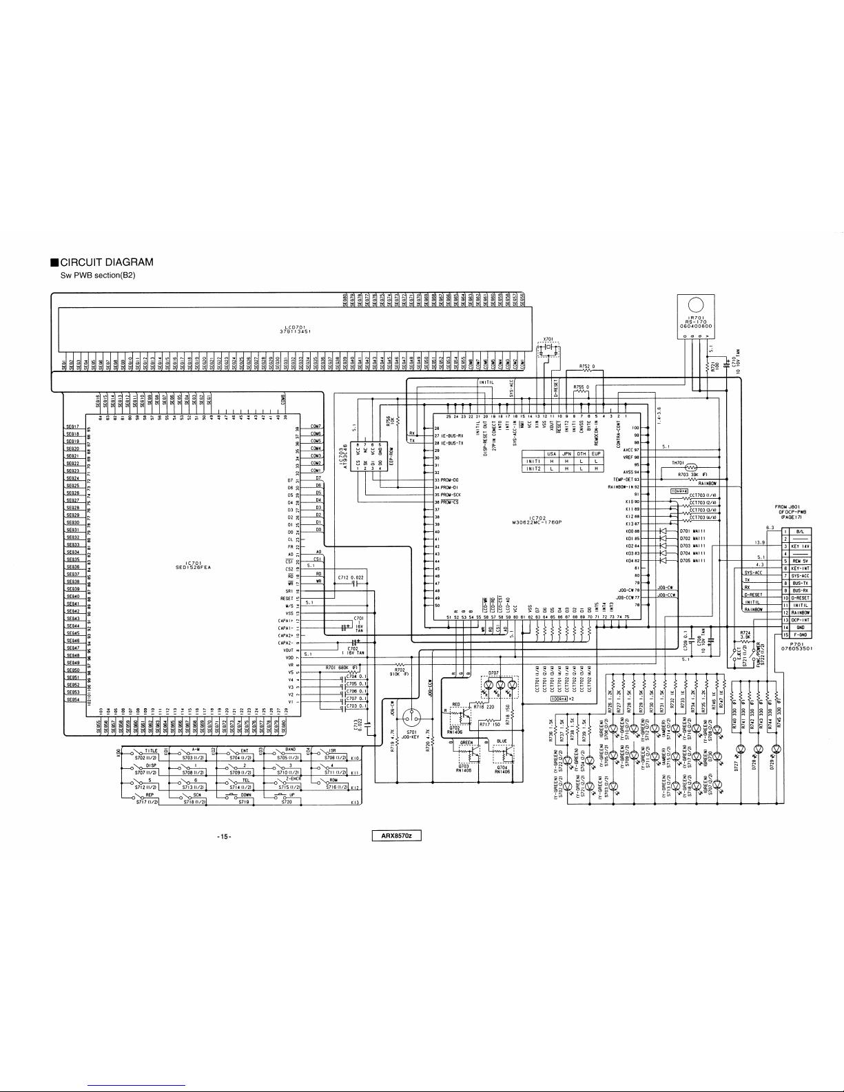
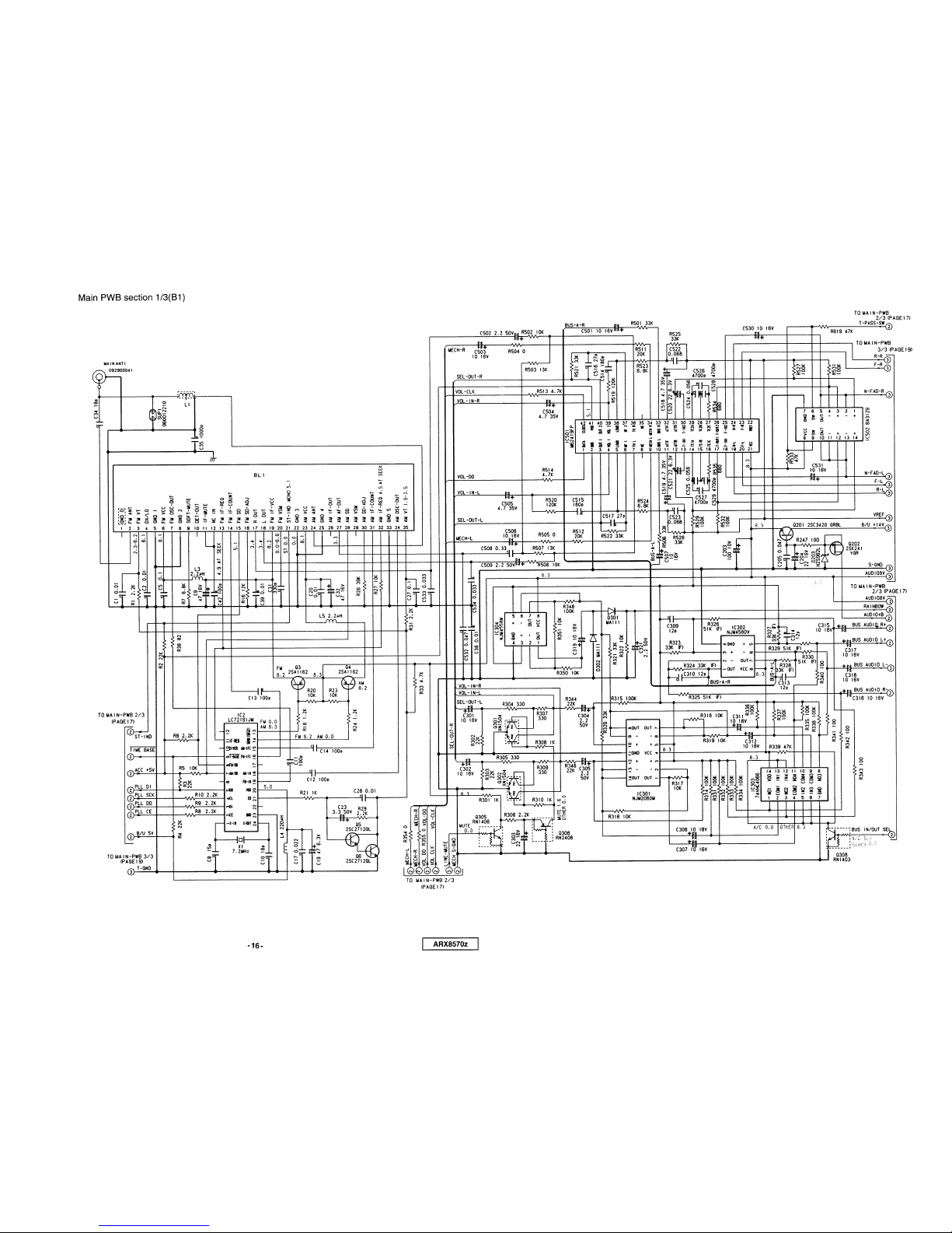


Table of contents
Other Clarion Cassette Player manuals


