COBHAM GR716-BOARD User manual

GR716-BOARD
Development Board
2019 User's Manual
T e most important t ing we build is trust
GR716-BOARD
Development Board
User's Manual
GR716-BOARD-UM, 2019, Version 0.1 www.cob am.com/gaisler

GR716-BOARD
Intentionally Blank
GR716-BOARD-UM, May 2019, Version 0.1 2 www.cob am.com/gaisler

GR716-BOARD
Table of Contents
1 Introduction......................................................................................................................5
1.1 Scope of the Document.......................................................................................5
1.2 Reference Documents..........................................................................................5
2 Abbreviations...................................................................................................................6
3 Introduction......................................................................................................................7
3.1 Overview.............................................................................................................
3.2 Handling..............................................................................................................8
4 Board Design....................................................................................................................
4.1 Board Block Diagram..........................................................................................9
4.2 Board Mechanical Configuration......................................................................10
4.3 GR 16 Microcontroller.....................................................................................13
4.4 Memory.............................................................................................................14
4.5 LVDS Interfaces................................................................................................14
4.6 GPIO..................................................................................................................15
4. Bootstrap Signals...............................................................................................15
4.8 Debug Support Unit Interfaces..........................................................................16
4.9 Oscillators and Clock Inputs.............................................................................1
4.10 Power Supply and Voltage Regulation..............................................................18
4.11 Reset Circuit and Button...................................................................................21
4.12 Watchdog...........................................................................................................21
5 Setting Up and Using the Board...................................................................................22
6 Interfaces and Configuration.......................................................................................23
6.1 List of Connectors.............................................................................................23
6.2 List of Oscillators, Switches and LED's............................................................25
7 Change Record...............................................................................................................30
GR716-BOARD-UM, May 2019, Version 0.1 3 www.cob am.com/gaisler

GR716-BOARD
List of Figures
Figure 3-1: GR 16-BOARD Development Board...............................................................................
Figure 4-1: GR 16-BOARD Board Block Diagram............................................................................9
Figure .4-2: GR 16-BOARD Board Dimensions..............................................................................10
Figure 4-3: GR 16-BOARD mounted on a GR 16-CPCI-DEV Carrier board.................................11
Figure 4-4: GR 16-TEST-MEMORY BOARD.................................................................................12
Figure 4-5: GR 16-TEST-ADCDAC BOARD..................................................................................12
Figure 4-6: GR 16 Microcontroller Block Diagram..........................................................................13
Figure 4- : GR 16 Package...............................................................................................................13
Figure 4-8: SPI Boot Memory Connections.......................................................................................14
Figure 4-9: Debug Support Unit connections.....................................................................................16
Figure 4-10: GR 16-DSU-USB Adapter............................................................................................16
Figure 4-11: Board level Clock Distribution Scheme........................................................................1
Figure 4-12: Power Regulation Scheme.............................................................................................19
Figure 4-13: Power Supply Configuration Jumpers...........................................................................20
Figure 6-1: PCB Top View.................................................................................................................26
Figure 6-2: PCB Bottom View...........................................................................................................2
Figure 6-3: PCB Top View (Photo)....................................................................................................28
Figure -1: PCB Bottom View (Photo)..............................................................................................29
List of Tables
Table 1: Bootstrap Resistor Settings...................................................................................................15
Table 2: List of Connectors................................................................................................................23
Table 3: J1 Screw Terminal Connector for Input Voltages.................................................................23
Table 4: J2 POWER – External Power Connector.............................................................................23
Table 5: Expansion connector P1 Pin-out...........................................................................................24
Table 6: Expansion connector P2Pin-out............................................................................................24
Table : List and definition of Oscillators and Crystals.....................................................................25
Table 8: List and definition of PCB mounted LED's..........................................................................25
Table 9: List and definition of Switches.............................................................................................25
Table 10: Definition of Switch S1 functions......................................................................................25
GR716-BOARD-UM, May 2019, Version 0.1 4 www.cob am.com/gaisler

GR716-BOARD
1 Introduction
1.1 Scope of the Document
This document provides a User's Manual and Interface document for the “GR 16-
BOARD” Development and Demonstration board.
The work has been performed by Cobham Gaisler AB, Göteborg, Sweden.
1.2 Reference Documents
[RD1] GR 16, Data Sheet and User's Manual",Cobham Gaisler, GR 16-UM-DS, available
from http://www.gaisler.com/index.php/products/components/GR 16
[RD2] GR 16-BOARD_schematic.pdf, Schematic
[RD3] GR 16-BOARD_assy_drawing.pdf, Assembly Drawing
[RD4] GRMON3 User's Manual, available from:
https://www.gaisler.com/index.php/products/debug-tools/grmon3
GR716-BOARD-UM, May 2019, Version 0.1 5 www.cob am.com/gaisler

GR716-BOARD
2 Abbreviations
ASIC Application Specific Integrated Circuit.
DSU Debug Support Unit
EDAC Error Detection and Correction
ESA European Space Agency
ESD Electro-Static Discharge
ESTEC European Space Research and Technology Center
GPIO General Purpose Input / Output
IC Integrated Circuit
I/O Input/Output
IP Intellectual Property
LDO Low Drop-Out
PCB Printed Circuit Board
POL Point of Load
SOC System On a Chip
SPW Spacewire
TBC To Be Confirmed
TBD To Be Defined
GR716-BOARD-UM, May 2019, Version 0.1 6 www.cob am.com/gaisler

GR716-BOARD
3 Introduction
3.1 Overview
This document describes the GR716-BOARD Development Board.
This equipment is intended to be used as a platform for the demonstration of the
Cobham Gaisler GR716 RAD Hard Microcontroller.
Furthermore, this board provides developers with a convenient hardware platform for
the evaluation and development of software for the GR716 microcontroller.
The GR716 Microcontroller features a fault-tolerant LEON3 SPARC V8 processor,
communication interfaces and on-chip ADC, DAC, Power-on-Reset, Oscillator, Brown-
out detection, LVDS transceivers, regulators to support for single 3.3V supply, ideally
suited for space and other high-rel applications.
The GR716 Microcontroller is a complex device with multifunctional pins whose
function depend on the mode of operation and programming of internal registers of the
device. This board treats the pins in a generic manner to allow easy access to all the pins
and features of the GR716 microcontroller
GR716-BOARD-UM, May 2019, Version 0.1 7 www.cob am.com/gaisler
Fig re 3-1: GR716-BOARD Development Board
GR716-BOARD
The board contains the following main items as detailed in section 4 of this document:
•size 80 x 100mm
•two 2x32 pin stackable 0.1” headers allowing access to all I/O pins
•connector for single VIN power input (+5V to +12V)
•alternative connector for connections to individual device power supplies
•jumpers for power supply configuration
•on-board regulators converting from VIN to 3.3V & 1.8V
•256 Mbit SPI memory (Cypress, S25FL256SAGN in 8 pin WSON package)
•socket for crystal (25MHz TBC)
•DIP switch for bootstrap settings
•on-board I2C voltage/current measurement
3.2 Handling
ATTENTION: OBSERVE PRECAUTIONS FOR
HANDLING ELECTROSTATIC SENSITIVE DEVICES
This unit contains sensitive electronic components which can be damaged by
Electrostatic Discharges (ESD). When handling or installing the unit observe
appropriate precautions and ESD safe practices.
When not in use, store the unit in an electrostatic protective container or bag.
When configuring the jumpers on the board, or connecting/disconnecting cables, ensure
that the unit is in an un-powered state.
When operating the board in a 'stand-alone' configuration, the power supply should be
current limited to prevent damage to the board or power supply in the event of an over-
current situation.
This board is intended for commercial use and evaluation in a standard laboratory
environment, nominally, 20°C. All devices are standard commercial types, intended for
use over the standard commercial operating temperature range (0 to 0ºC).
GR716-BOARD-UM, May 2019, Version 0.1 8 www.cob am.com/gaisler
GR716-BOARD
4 Board Design
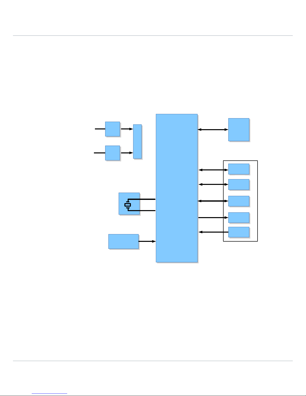
4.1 Board Block Diagram
The GR716-BOARD Board provides the electrical functions and interfaces as represented
in the block diagram, Figure .4-2.
Note that not all features and interfaces are available at the same time, and the
configuration of on-board resistors plus programming of registers is required to access
some of the features.
GR716-BOARD-UM, May 2019, Version 0.1 9 www.cob am.com/gaisler
Fig re 4-1: GR716-BOARD Board Block Diagram
CRYSTAL
CRYSTAL
GR716
MICRO-
CONTROLLER
GR716
MICRO-
CONTROLLER
RESET_OUT
RESET_OUT
EXPANSION CONNECTOR
DCDC
DCDC SPI
FLASH
SPI
FLASH
GPIO
GPIO
DSU
DSU
BOOTSTRAP/
CONFIGURATION
BOOTSTRAP/
CONFIGURATION
3.3V
RESET_IN
RESET_IN
DCDC
DCDC
1.8V
VIN
VIN
LVDS
LVDS
CONFIGURATION
UMPERS
CONFIGURATION
UMPERS

GR716-BOARD
4.2 Board Mechanical Configuration
The board (80 x 100mm) and can be used 'stand-alone' on the bench-top simply an
external +5V power supply connected to connector J2.For mounting of the board on a
carrier or expansion board, four M2.5 mounting holes are provided in the corners of the
board, as shown in the figure below.
The expansion connectors P1 and P2 of the GR716-BOARD are stacking style
connectors having a socket on the bottom side and an extended pin on the top side. In a
stand-alone configuration the pins on the top side allow easy access for Logic Analyser
or Oscilloscope probing for all the functional microcontroller pins.
GR716-BOARD-UM, May 2019, Version 0.1 10 www.cob am.com/gaisler
Fig re .4-2: GR716-BOARD Board Dimensions
Other manuals for GR716-BOARD
1
Table of contents
Other COBHAM Motherboard manuals

COBHAM
COBHAM GR716-CPCI-DEV User manual

COBHAM
COBHAM GR-CPCI-GR740 User manual

COBHAM
COBHAM SPSC-EVB-R0 User manual

COBHAM
COBHAM GR716-MINI User manual

COBHAM
COBHAM CAES UT65CML8X8FD-EVB-UM User manual

COBHAM
COBHAM GR712RC User manual

COBHAM
COBHAM GR-CPCI-GR740 User manual

COBHAM
COBHAM GR-VPX-GR740-BOARD User manual


